Article

Effects on the Surface and Luminescence Properties of GaAs by SF6 Plasma Passivation

1
State Key Laboratory of High Power Semiconductor Lasers, Changchun University of Science and Technology, Changchun 130022, China
2
Jilin Provincial Key Laboratory of Architectural Electricity & Comprehensive Energy Saving, School of Electrical Engineering and Computer, Jilin Jianzhu University, Changchun 130118, China
*
Author to whom correspondence should be addressed.
Crystals 2018, 8(9), 339; https://doi.org/10.3390/cryst8090339
Submission received: 17 July 2018 / Revised: 18 August 2018 / Accepted: 19 August 2018 / Published: 23 August 2018
(This article belongs to the Section Crystal Engineering)

Abstract

:
The passivation effects of the SF6 plasma on a GaAs surface has been investigated by using the radio frequency (RF) plasma method. The RF’s power, chamber pressure, and plasma treatment time are optimized by photoluminescence (PL), atomic force microscopy (AFM), and X-ray photoelectron spectroscopy (XPS). The PL intensity of passivated GaAs samples is about 1.8 times higher than those which are untreated. The oxide traps and As-As dimers can be removed effectively by using SF6 plasma treatment, and Ga-F can form on the surface of GaAs. It has also been found that the stability of the passivated GaAs surface can be enhanced by depositing SiO2 films onto the GaAs surface. These indicate that the passivation of GaAs surfaces can be achieved by using SF6 plasma treatment.

1. Introduction

GaAs is a kind of typical III-V group of semiconductor materials with a large direct band gap, high carrier mobility, and superior thermal stability, which is widely used for the fabrication of semiconductor lasers, solar batteries, ultraviolet photodetectors, etc. However, impurity defects and oxide layers are easily formed on GaAs surfaces due to the combination of GaAs and oxygen in the oxygen-containing atmosphere. The high interface trap density (Dit), caused by the surface oxide layer, has the effect of scattering a nonradiative recombination for carriers [1,2], and also causes Fermi level pinning, thus having a pronounced effect on the optical and electrical properties of GaAs semiconductor devices [3].
The traditional passivation for GaAs is mainly based on wet passivation by sulfur-containing solutions [4,5,6,7], which can form a thin layer of sulfide to saturate part of the dangling bonds, and to remove native oxides on GaAs surfaces effectively. Although this passivation method can reduce the surface nonradiative recombination, the thin sulfur passivation layer is not stable in an atmospheric environment and the passivation effect will obviously degrade in a short period of time. Furthermore, the requirement for subsequent device process is strict, so there are obvious limitations in the practicability of GaAs surface passivation by sulfur-containing solutions [8]. Ar plasma treatment is also used to clean GaAs surface effectively and improve the binding energy on the surface. However, Ar plasma treatment can cause serious surface damage to GaAs materials due to high energy Ar ion bombardment. Fluorine-based plasma is reported to be another good way for passivating the GaAs surface, because it is capable of passivating the oxygen vacancies by CF4 [9,10] and SF6 [11,12,13,14]. As a greenhouse gas, CF4 can pollute the atmosphere and generate carbon pollution on semiconductor surfaces [9]. Previous reports show that GaF3 formed on SF6-treated GaAs surfaces [14] have a stable interface and a low density of interfacial states. However, the passivation effect of GaAs characterized by PL has not been reported yet, and the PL characterization is one of the most important aspects for GaAs surface passivation.
In this work, we report fluorine and sulfur plasma incorporation on GaAs surfaces by a glow discharge in SF6 ambience. Because of the high electronegativity of fluorine ions, it may substitute oxygen vacancy sites and dangling bonds on GaAs surfaces. The passivation effect by SF6 plasma under different RF powers, chamber pressures, and plasma treatment times has been studied in detail by PL, AFM, and XPS measurements.

2. Experiment

In this experiment, plasma passivation of a GaAs surface was carried out using JCP-350 type RF plasma equipment. (100) oriented n-type GaAs wafers doped with Si (2.4 × 1018 cm−3), were used for GaAs surface passivation experiments. First, the GaAs wafer was cut into small samples with a size of 2 cm × 2 cm, and ultrasonic cleaning with toluene, acetone, and methanol for 10 min, respectively, was used to remove organic contamination on the GaAs surface. This was followed by a large amount of deionized water rinsing, and then it was dried by using a nitrogen gas blow.
Next, an ultrasonic treatment in 30% HF solution was used to remove the thick oxide layer on the GaAs surface. PL measurement for each GaAs sample was done before and after plasma treatment to obtain the PL intensity change by plasma passivation. Then, SF6 (99.999%) was inlet into the vacuum chamber by the gas flow meter when the chamber vacuum reached 5 × 10⁻⁴ Pa, and the plasma was provided with a 13.56 MHz RF source. The temperature of GaAs samples on sample stage was set at 250 °C. The ion energy, flux of plasma, and treatment time were adjusted to remove surface contamination on GaAs samples effectively, which was mainly influenced by processing conditions. Finally, the passivation effect on the GaAs surface by SF6 plasma under different RF powers, chamber pressures, and plasma treatment times were discussed. The main process parameters are listed in Table 1.
The photoluminescence spectrum of GaAs samples was measured by using the HR2000+ spectrometer (Ocean Optics, Inc., Largo, FL, USA), and the excitation light source was a 660 nm wavelength semiconductor laser with an output power of 1~100 mW. The surface morphology was observed by Agilent 5500 atomic force microscopy (Agilent Technologies, Inc., Santa Clara, UT, USA), and the chemical composition of the passivated surface was analyzed through ESCALAB-MKII X-ray photoelectron spectroscopy (VG Thermo Scientific Ltd., West Sussex, UK).

3. Measurement and Analysis

3.1. RF Power Effect

Nonradiative recombination centers can be created by introducing defect energy levels into the GaAs band gap in the oxidation process of the GaAs surface. Therefore, the effect of surface passivation can be evaluated by the PL intensity measurement of the GaAs intrinsic emission peak. The higher the PL intensity, the less the defects exist on the surface, and the better the passivation can be achieved.
The effect of RF power on PL intensity of passivated GaAs by SF6 plasma is shown in Figure 1. When the RF power is below 10 W, PL intensity increases slowly because of the low SF6 ion energy and flux. When the RF power increases to higher than 10 W, high ion energy and ion flux density of SF6 can be obtained for strong surface bombardment and reaction, and the passivation effect by SF6 plasma increases gradually. It can be seen in Figure 1 that the PL intensity of samples is about 1.63 times higher than untreated when the RF power reaches 100 W. With a further increase in RF power, the intensity of PL begins to decrease, and defects caused by strong ion bombardment to the sample surface is the major reason for PL deterioration.

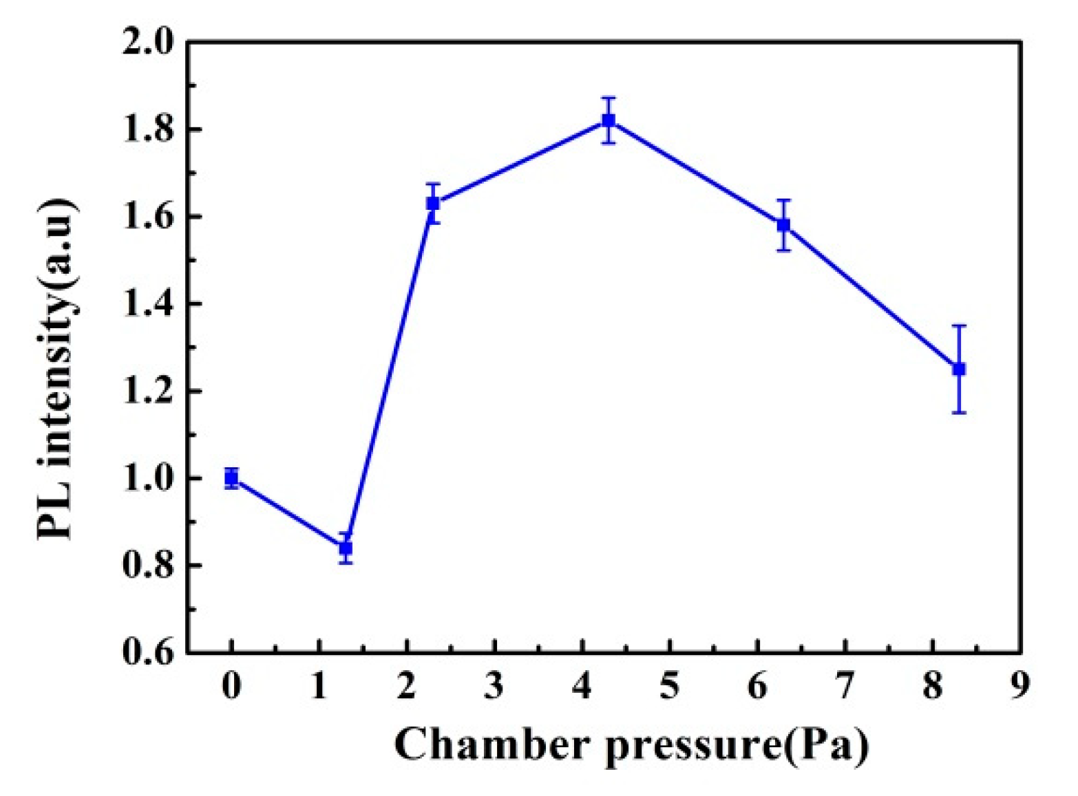
3.2. Chamber Pressure Effect

Figure 2 shows the effect of chamber pressure on the PL intensity of passivated GaAs by SF6 plasma. It has been shown that the maximum PL increase is achieved at a chamber pressure of 4.3 Pa. When the chamber pressure is small, the density of SF6 in the plasma chamber is low, and as a result, the low-density SF6 plasma and high ion energy will give a weak passivation on the GaAs surface. Because ion bombardment defects may obviously deteriorate the GaAs surface, the PL intensity increases a little at low chamber pressure. With a further increase to the chamber pressure, the PL obviously enhances. When the chamber pressure reaches 4.3 Pa, the PL intensity has the maximum increasing. While the chamber pressure exceeds 4.3 Pa, the SF6 density in the chamber becomes high and the collision probability among the energetic charged ions increases greatly, resulting in the energy loss of plasma ions. Thus, the PL intensity becomes low for samples by high chamber pressure, due to the low ion kinetic energy.

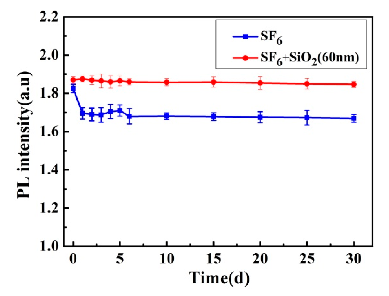
3.3. Plasma Treatment Time Effect

Figure 3 shows the measurement results of PL intensity versus plasma treatment time. It can be seen that when the plasma treatment time is in the range of 0–5 min, the PL intensity increases with the plasma treatment time, which means that oxides on GaAs surface can be effectively removed and the non-radiative recombination centers caused by oxide-related surface states will reduce greatly at the beginning of plasma treatment. The As–S composition may form on the GaAs surface when the plasma treatment time exceeds 5 min, although the As–S begins to decompose at 250 °C, and the intensity of PL will then tend to decrease due to the bombardment damage caused by stimulated ions.
The surface morphology of treated GaAs samples was measured by using AFM. Figure 4 shows the AFM images of the GaAs samples by SF6 plasma treatment with different time durations of 0 min, 5 min, and 10 min, respectively. The root mean square (RMS) roughness of the untreated GaAs surface is 0.148 nm, as shown in Figure 4a. The SF6 plasma-treated surface gives a relative low RMS roughness of 0.145 nm when the plasma treatment time is 5 min, as shown in Figure 4b. A large RMS roughness of 23.9 nm with obvious surface nanoparticles can be found when the plasma treatment time increases to 10 min, as shown in Figure 4c. This phenomenon may be caused by two reasons—firstly, the lattice mismatch of several surface compositions could have resulted in a poor surface morphology; and secondly, F and S ions bombarding the surface with continued passivation may eventually lead to a cluster-like migration on the GaAs surface.
The processed GaAs surface was also analyzed via XPS for its composition, valence state, and other physical information. XPS is a typical surface analysis technique with a shallow detection depth of 2–4 nm. F 1s, S 2p, Ga 3d, and As 3d photoelectron spectra of SF6 plasma-treated GaAs samples were measured for GaAs samples with a treatment time of 0 min, 5 min and 10 min, respectively. Figure 5a and Figure 6a show the XPS of As 3d and Ga 3d of the samples by SF6 plasma treatment. In Figure 5a, the Ga–As, As–As, and As–O peaks are found at 40.84 eV [15], 41.55 eV [5], and 44.27 eV [15,16], respectively, and in Figure 6a, the As–Ga, Ga2O, and Ga2O3 peaks appear at 19.14 eV [15], 20.24 eV [1], and 20.57 eV [17], respectively. It can be seen that the surface oxidation is severe for untreated GaAs surfaces. As–As and Ga–O peaks disappear completely for 5 min treatment samples, which indicates that the oxide traps and As–As dimers can be removed at optimized SF6 plasma treatment conditions, and a small amount of GaF3 (20.34 eV) [15] has formed on GaAs surface. GaF3 has good physical and chemical stability, and its large band gap (9.8 eV) plays a very important role in eliminating surface absorption, oxidation, and other significant factors that seriously affects the performance and lifespan of GaAs-based optoelectronic devices [18]. In addition, As–F (AsF3, AsF5) may also form in the process, but gaseous As–F will not be detected in the XPS measurement. GaF3 (20.54 eV) and As2S3 (44.49 eV) begin to form on the GaAs surface when the SF6 plasma treatment time is up to 10 min, as shown in Figure 5a and Figure 6a. The GaAs peak is not detectable due to the thick surface layer.
Figure 5b and Figure 6b show the XPS of S 2p and F 1s of the samples. The peak at 160.07 eV in the S 2p diagram of the untreated GaAs surface is Ga 3s, according to previous research [19,20]. In the S 2p and F 1s XPS measurement of GaAs samples by 5 min SF6 plasma treatment, peaks of Ga 3s (160.37 eV) and GaF3 (685.1 eV) [13] are detectable, and the As-S peak is not found. As2S3 (162.42 eV) begins to form, and the GaF3 (685.3 eV) continues to increase when the treatment time is up to 10 min, which is consistent with the measurement result of As 3d and Ga 3d XPS spectra.
For the GaAs sample by 5 min treatment, the As–Ga and Ga–As peaks shift to 41.34 eV and 19.44 eV, respectively. A 0.3 eV blue shift of XPS peaks shows that the chemical environment of the GaAs surface is changed, due to the formation of Ga-F bonds and the passivation of the GaAs surface dangling bonds by F atoms [9,13,21]. It can be seen from Figure 5b that the Ga 3s peak also has a similar blue shift of 0.3 eV. From Figure 5b and Figure 6a,b, it is found that XPS peaks of Ga 3s and GaF3 also have a blue shift of 0.2 eV, caused by a prolonged plasma treatment for 10 min.
It can also be known that the poor surface morphology of the sample by 10 min treatment is caused due to the lattice mismatch of As–S and Ga–F, as shown in Figure 4c. Therefore, the GaAs surface by SF6 plasma treatment for an appropriate duration (as for 5 min) may exhibit favorable structural properties and chemical bonding conditions, which is beneficial to the subsequent device process.
The optimized process condition for GaAs surface passivation by SF6 plasma was obtained by the experiments above, where it is shown that the maximum PL intensity is achieved at an RF power of 100 W, chamber pressure of 4.3 Pa, and treatment time of 5 min, respectively. The contrast of PL plots between passivated and untreated GaAs samples is shown in Figure 7. It can be seen that the PL intensity of the GaAs surface passivated by SF6 plasma treatment is about 1.8 times higher than that of untreated.
A SiO2 coating on a passivated GaAs surface was done to improve the stability of the passivation layer by RF sputtering. Samples with different thicknesses of SiO2 were prepared to test the anti-reflection effect, as shown in Figure 8. The PL intensity is only about 1.05 times higher than untreated when the SiO2 film is about 60 nm thick, which implies that a thin SiO2 coating below 60 nm has little influence on the PL intensity measurement.
Finally, a 60 nm-thick SiO2 coating was chosen as the surface protective film to study the PL stability of passivated GaAs samples for a 30-day duration in the open air. The PLs of samples with and without SiO2 coatings were measured at room temperature. As shown in Figure 9, the PL intensity of SF6 plasma-treated GaAs samples without an SiO2 coating drops fast at about 24 h, and then tends to remain stable. The PL intensity of samples with an SiO2 coating remains nearly unchanged for the whole 30-day duration of the experiment.

4. Conclusions

The (100) oriented GaAs samples were passivated by SF6 plasma treatment using the RF method. RF power and chamber pressure were optimized by PL characterization, and the PL intensity shows a maximum increase at an RF power of 100 W and chamber pressure of 4.3 Pa. It is also shown that the treatment time has a great influence on GaAs surface passivation. PL, AFM, and XPS were used to analyze the effect of treatment time on passivation. It was found that the PL emission intensity was highest when the plasma treatment time was optimized to 5 min. AFM measurement shows a lower surface roughness by 5 min-treated samples, compared with the 10 min samples. At the same time, XPS measurement indicates that the surface oxide and As-As dimers can be effectively removed. Furthermore, GaF3 is formed on the GaAs surface, which can obviously reduce surface deterioration. By optimizing the experimental conditions for SF6 plasma treatment, the PL intensity of GaAs samples is about 1.8 times higher than untreated. A slightly longer plasma treatment of SF6 to the GaAs surface will result in more complicated surface compositions and obviously deteriorate surface morphology, which is not beneficial to subsequent device processes. Finally, it has been shown that a thin SiO2 coating with a thickness of 60 nm has a good effect on the PL stability of the passivated GaAs samples.

Author Contributions

Conceptualization, Y.X. and B.B.; Methodology, Y.X. and X.G.; Validation, X.G., Z.Q. and J.Z.; Formal Analysis, Y.X.; Investigation, B.B.; Resources, X.G., L.Z. and Z.Q.; Data Curation, Y.X., X.Z. and L.Z.; Writing-Original Draft Preparation, Y.X.; Writing-Review & Editing, Y.X. and B.B.; Visualization, Y.X., X.Z. and J.Z.; Supervision, B.B.; Project Administration, B.B.; Funding Acquisition, B.B.

Funding

This work was supported by National Key R&D Project (No. 2017YFB0405100), National Natural Science Foundation of China (No. 61774024), Jilin province science and technology development plan (No. 20150203007GX, 20160203017GX, 20170101047JC, 20170203014GX), Science and Technology Development Project of Jilin Province, China (No. 20170520169JH).

Conflicts of Interest

The authors declare no conflict of interest.

References

  1. Lu, H.; Xu, J.; Liu, L.; Wang, L.; Lai, P.; Tang, W. Improved interfacial quality of GaAs metal-oxide-semiconductor device with NH3-plasma treated yittrium-oxynitride as interfacial passivation layer. Microelectron. Reliab. 2016, 56, 17–21. [Google Scholar] [CrossRef]
  2. Edmonds, M.; Kent, T.; Chagarov, E.; Sardashti, K.; Droopad, R.; Chang, M.; Kachian, J.; Park, J.H.; Kummel, A. Passivation of InGaAs (001)-(2 × 4) by self-limiting chemical vapor deposition of a silicon hydride control layer. J. Am. Chem. Soc. 2015, 137, 8526–8533. [Google Scholar] [CrossRef] [PubMed]
  3. Dalapati, G.K.; Tong, Y.; Loh, W.Y.; Mun, H.K.; Cho, B.J. Impact of interfacial layer control using Gd2O3 in HfO2 gate dielectric on GaAs. Appl. Phys. Lett. 2007, 90, 1897–1904. [Google Scholar] [CrossRef]
  4. Lebedev, M.V.; Kunitsyna, E.V.; Calvet, W.; Mayer, T.; Jaegermann, W. Sulfur passivation of GaSb (100) surfaces: Comparison of aqueous and alcoholic sulfide solutions using synchrotron radiation photoemission spectroscopy. J. Phys. Chem. C 2013, 117, 15996–16004. [Google Scholar] [CrossRef]
  5. Ghita, R.; Negrila, C.; Cotirlan, C.; Logofatu, C. On the passivation of GaAs surface by sulfide compounds. Dig. J. Nanomater. Bios. 2013, 8, 1335–1344. [Google Scholar]
  6. Lucero, A.T.; Byun, Y.-C.; Qin, X.; Cheng, L.; Kim, H.; Wallace, R.M.; Kim, J. Formation of a ZnO/ZnS interface passivation layer on (NH4)2S treated In0.53Ga0.47As: Electrical and in-situ X-ray photoelectron spectroscopy characterization. J. Appl. Phys. 2016, 55, 08PC02. [Google Scholar] [CrossRef]
  7. Kim, S.-H.; Kim, G.-S.; Kim, J.-K.; Park, J.-H.; Shin, C.; Choi, C.; Yu, H.-Y. Fermi-level unpinning using a Ge-passivated metal-interlayer-semiconductor structure for non-alloyed ohmic contact of high-electron-mobility transistors. IEEE Electron Device Lett. 2015, 36, 884–886. [Google Scholar] [CrossRef]
  8. Lambert, R.W.; Ayling, T.; Hendry, A.F.; Carson, J.M.; Barrow, D.A.; McHendry, S.; Scott, C.J.; McKee, A.; Meredith, W. Facet-passivation processes for the improvement of Al-containing semiconductor laser diodes. J. Lightw. Technol. 2006, 24, 956–961. [Google Scholar] [CrossRef]
  9. Iida, M.; Kaibe, H.T.; Okumura, T. Low-temperature fluorination of GaAs surface by CF4 plasma. J. Appl. Phys. 1991, 30, 1581–1584. [Google Scholar] [CrossRef]
  10. Taniguchi, M.; Murakawa, T.; Kajitani, Y. A novel passivation technique of GaAs power MESFETs. Appl. Surf. Sci. 1992, 56, 827–831. [Google Scholar] [CrossRef]
  11. Kim, G.-S.; Kim, S.-H.; Kim, J.-K.; Shin, C.; Park, J.-H.; Saraswat, K.C.; Cho, B.J.; Yu, H.-Y. Surface passivation of germanium using SF6 plasma to reduce source/drain contact resistance in germanium n-FET. IEEE Electron Device Lett. 2015, 36, 745–747. [Google Scholar]
  12. Kim, S.-H.; Kim, G.-S.; Kim, S.-W.; Kim, J.-K.; Choi, C.; Park, J.-H.; Choi, R.; Yu, H.-Y. Non-alloyed ohmic contacts on gaas using metal-interlayer-semiconductor structure with SF6 plasma treatment. IEEE Electron Device Lett. 2016, 37, 373–376. [Google Scholar] [CrossRef]
  13. Polydorou, E.; Zeniou, A.; Tsikritzis, D.; Soultati, A.; Sakellis, I.; Gardelis, S.; Papadopoulos, T.A.; Briscoe, J.; Palilis, L.C.; Kennou, S. Surface passivation effect by fluorine plasma treatment on ZnO for efficiency and lifetime improvement of inverted polymer solar cells. J. Mater. Chem. A 2016, 4, 11844–11858. [Google Scholar] [CrossRef] [Green Version]
  14. Dittrich, T.; John, S.; John, W. Characterization of the n-GaAs surface after CF4, SF6, CCl2F2, and CCl2F2:O2 plasma treatment by photoreflectance. Phys. Status Solidi 1991, 128, 435–446. [Google Scholar] [CrossRef]
  15. Budz, H.; Biesinger, M.; LaPierre, R. Passivation of GaAs by octadecanethiol self-assembled monolayers deposited from liquid and vapor phases. J. Vac. Sci. Technol. B Nanotechnol. Microelectron. Mater. Process. Meas. Phenom. 2009, 27, 637–648. [Google Scholar] [CrossRef]
  16. Li, Y.; Wee, A.; Huan, C.; Zheng, J. Ion-induced nitridation of GaAs (100) surface. Appl. Surf. Sci. 2001, 174, 275–282. [Google Scholar] [CrossRef]
  17. Ruppalt, L.B.; Cleveland, E.R.; Champlain, J.G.; Bennett, B.R.; Boos, J.B.; Prokes, S.M. Electronic properties of atomic-layer-deposited high-k dielectrics on GaAb (001) with hydrogen plasma pretreatment. J. Vac. Sci. Technol. B Nanotechnol. Microelectron. Mater. Process. Meas. Phenom. 2015, 33, 04E102-5. [Google Scholar]
  18. Varekamp, P.; Simpson, W.; Shuh, D.; Durbin, T.; Chakarian, V.; Yarmoff, J. Electronic structure of GaF3 films grown on GaAs via exposure to XeF2. Phys. Rev. B 1994, 50, 14267. [Google Scholar] [CrossRef]
  19. Marshall, G.M.; Lopinski, G.P.; Bensebaa, F.; Dubowski, J.J. Surface dipole layer potential induced IR absorption enhancement inn-alkanethiol sams on GaAs (001). Langmuir 2009, 25, 13561–13568. [Google Scholar] [CrossRef] [PubMed]
  20. Huang, X.; Dubowski, J.J. Solvent-mediated self-assembly of hexadecanethiol on GaAs (001). Appl. Surf. Sci. 2014, 299, 66–72. [Google Scholar] [CrossRef]
  21. Liu, L.N.; Choi, H.W.; Xu, J.P.; Lai, P.T. Passivation of oxide traps and interface states in GaAs metal-oxide-semiconductor capacitor by LaTaON passivation layer and fluorine incorporation. Appl. Phys. Lett. 2015, 107, 213501. [Google Scholar] [CrossRef]
Figure 1. The influence of radio frequency (RF) power on photoluminescence (PL) intensity.
Crystals 08 00339 g001
Figure 2. The influence of chamber pressure on PL intensity.
Crystals 08 00339 g002
Figure 3. The influence of plasma treatment time on PL intensity.
Crystals 08 00339 g003
Figure 4. Atomic force microscopy (AFM) images of the GaAs surface by SF6 plasma treatment. (a) Without treatment; (b) 5 min and (c) 10 min.
Crystals 08 00339 g004
Figure 5. X-ray photoelectron spectroscopy (XPS) analysis of the GaAs surface using different SF6 plasma treatment for 0 min, 5 min, and 10 min, (a) As 3d and (b) S 2p.
Crystals 08 00339 g005
Figure 6. XPS analysis of the GaAs surface by using different SF6 plasma treatment for 0 min, 5 min, and 10 min, (a) Ga 3d and (b) F 1s.
Crystals 08 00339 g006
Figure 7. The PL intensity of GaAs samples prepared by an optimized passivation process.
Crystals 08 00339 g007
Figure 8. The influence of SiO2 thickness on PL intensity.
Crystals 08 00339 g008
Figure 9. The stability of GaAs PL intensity in open air.
Crystals 08 00339 g009
Table 1. The process parameters for passivation.
ParameterValue
SF6 Gas purity 99.999%
Background vacuum 2.8 × 10⁻⁴ Pa
RF power10–180 W
Chamber pressure 0.3–8.3 Pa
Treatment time1–60 min
SF6/N2 gas flow rate18/6 sccm
Sample temperature250 °C

