Article

Effect of the Ultrasonic Substrate Vibration on Nucleation and Crystallization of PbI2 Crystals and Thin Films

1
State Key Laboratory for Modification of Chemical Fibers and Polymer Materials, College of Materials Science and Engineering, Donghua University, Shanghai 201620, China
2
University of Michigan-Shanghai Jiao Tong University Joint Institute, Shanghai 200240, China
*
Author to whom correspondence should be addressed.
Crystals 2018, 8(2), 60; https://doi.org/10.3390/cryst8020060
Submission received: 18 December 2017 / Revised: 23 January 2018 / Accepted: 24 January 2018 / Published: 26 January 2018

Abstract

:
Preparation of defect-free and well-controlled solution-processed crystalline thin films is highly desirable for emerging technologies, such as perovskite solar cells. In this work, using PbI2 as a model solution with a vast variety of applications, we demonstrate that the excitation of a liquid thin film by imposed ultrasonic vibration on the film substrate significantly affects the nucleation and crystallization kinetics of PbI2 and the morphology of the resulting solid thin film. It is found that by applying ultrasonic vibration to PbI2 solution spun onto an ITO substrate with a moderate power and excitation duration (5 W and 1 min for the 40 kHz transducer used in this study), the nucleation rate increases and the crystals transform from 2D or planar to epitaxial 3D columnar structures, resulting in the suppression of crystallization dewetting. The effects of various induced physical phenomena as a result of the excitation by ultrasonic vibration are discussed, including microstreaming and micromixing, increased heat transfer and local temperature, a change in the thermodynamic state of the solution, and a decrease in the supersaturation point. It is shown that the ultrasonic-assisted solution deposition of the PbI2 thin films is controllable and reproducible, a process which is low-cost and in line with the large-scale fabrication of such solution-processed thin films.

1. Introduction

Crystalline materials are frequently used in traditional applications, such as silicon-based semiconductors, as well as emerging molecular semiconducting devices, owing to their tunable physical and chemical properties and the ease of processing. The functional properties of the crystalline substances, such as their band gap, electrical and thermal conductivity, transparency, and chemical and thermal stability are not only dependent of the chemical composition and the basic crystal structure, but also depend on the characteristics of their crystallites, such as size and size distribution, preferential orientation, alignment, and number density [1,2,3,4,5,6,7,8]. This work focuses on the nucleation and crystallization of lead iodide (PbI2), a semiconductor with numerous applications. Small and compact PbI2 crystallites preferentially developed along the (001) plane can provide low electrical resistivity and large band gap, suitable for sensor development [5,9], and the layered and planar PbI2 is suitable for the development of flexible detectors [10]. In addition, PbI2 is a major precursor for the fabrication of methylammonium lead perovskite solar cells [11], using a two-step deposition method, in which a PbI2 thin film is deposited first, which serves as a template for the deposition of the second precursor [6,8,12,13].
Thin films are deposited either from the vapor phase or a liquid solution, where the latter is a simple and cost-effective process, but suffers from poor reproducibility and the presence of defects. It has been shown that the 2D-grown PbI2 films with poor grain boundaries may render high sheet resistivity and weak optical responses, due to the large number of charge-trapping sites [14]. Additionally, coexistence of multiple phases or amorphous areas in the PbI2 matrix may hinder the performance of the associated devices [15]. Achieving intact, defect-free, and reproducible solution-processed thin film entails careful control of all aspects of the deposition process to yield a desired thin solid film [16]. Crystalline thin films are even more challenging to fabricate compared to the amorphous films, because the complex spatial geometry of the crystallites in such films may affect the film integrity and roughness. Most of the relevant studies have considered thermal annealing, chemical treatments, and solution engineering for controlling the crystal growth during the deposition, e.g., [17,18,19], with varying degrees of success, and at the expense of incurring additional costs and environmental footprint. In this context, Habibi et al. [19] examined solution deposition of PbI2 thin films and tuned the process parameters to suppress the phenomenon of dewetting caused by crystallization (crystallization dewetting). In the absence of crystallization dewetting, an intact and pinhole-free thin film can form. It was stated that dewetting can be induced by crystallization due to the consumption of the solute from the diffusion layers adjacent to the growing crystallites during solvent evaporation (Figure 1). While crystallization dewetting, which has a geometrical nature, occurs only in thin liquid films of ionic solutions, general mechanisms of liquid film dewetting, such as spinodal dewetting due to the long range intermolecular effects, heterogeneous dewetting due to impurities, and homogenous nucleation due to the presence of the thermal shocks may cause dewetting and film rupture, as well [19,20,21,22]. Therefore, phase change due to seed formation may trigger microscopic heterogeneous dewetting, and consumption of the solute and growth of large crystallites in the film may create protruded crystallites causing macroscopic crystallization dewetting.
In this work, instead of employing the traditional means of controlling the crystal growth, such as chemical and thermal treatments, ultrasonic vibration is imposed on the substrate of the wet-spun films, in order to achieve fine crystallites with no pinholes and dewetted areas in the thin film. This process resembles the well-known epitaxial growth in the vapor-deposition of thin films. Imposed vibration may affect a thin film of an ionic solution, such as PbI2, in two ways: firstly, it may affect the stability of the thin liquid or wet film, while there is still no significant phase change; secondly, it may affect the crystal growth during the phase change, where the former has been investigated in various works [23,24,25,26,27], whereas the latter entails more fundamental studies. Eslamian [27] provides a complete literature review on the effect of acoustic vibration in bulk and thin liquid films, including ionic solutions. Here, some representative works are reviewed. In bulk materials, acoustic (ultrasonic) vibration has been used to control the crystallization of fine-grained, homogenous, and dense ingots from molten solution of metals and semiconductors, e.g., [28,29,30], to the drying of fruits [31]. In brief, the generation and collapse of cavitation bubbles act as nucleation sites for crystallization, and flow streaming and agitation results in a decrease in the crystal size and homogenized composition of the product. In the area of sonochemical synthesis of nanomaterials, some workers have studied the effect of vibration on crystallinity. For instance, Gielen et al. [32] used ultrasonic vibration to control the crystallization and agglomeration of pharmaceutical particles grown in solution, concluding that controlled ultrasonic vibration assists the generation of nuclei and suppresses agglomeration, but prolonged or intensive vibration may damage and fracture the crystals. In thin films, some earlier works have focused on vibration-assisted chemical bath deposition of ceramic thin films, e.g., [33], where it was observed that the sonication of the bulk solution results in the higher crystallinity, lower roughness, higher density, and superior properties of the resulting solid thin films. In the area of thin film deposition using casting methods, Diemer et al. [34] generated low-frequency acoustic vibrations transmitted through air to the thin film of a polymer solution to tune the film crystallinity and nanostructure to fabricate high-performance organic thin film transistors. In a facile approach, we employed a 40 kHz ultrasonic transducer mounted inside of a metal box that also worked as the sample holder. In this method, the ultrasonic vibrations of the substrate are transmitted to the wet film. The method was employed to adjust and improve the crystallinity and homogeneity of various thin films, e.g., graphene-titania photocatalyst film [35], polymeric films [36,37,38], as well as the crystallinity of PbI2 and perovskite films [39,40,41]. It was concluded that the imposed vibration with proper amplitude and excitation duration has two major effects: firstly, it improves the uniformity and homogeneity of the composition of the resulting solution-processed thin solid film, because of the induced microstreaming in the liquid films [26] and, secondly, it controls the crystallization kinetics.
The foregoing introduction and literature review reveal that while there are several examples on the development of high-performance thin films using imposed acoustic vibration and the area is expanding quickly: there is little fundamental research on the effect of the acoustic or ultrasonic vibration on the crystallization kinetics. Thus, in this work, the aforementioned problem will be studied on spun-on wet films of PbI2 in dimethyl formamide (DMF) subjected to 40 kHz ultrasonic vibration at varying vibration powers and time durations. We will show that a well-controlled imposed vibration results in an enhanced nucleation rate, confinement of the crystal growth, suppression of aggregation and dewetting induced by crystallization, and uniform distribution of the crystallites in the thin film.

2. Materials and Methods

All materials were purchased from Sigma-Aldrich (St. Louis, MI, USA). Indium-tin oxide (ITO)-coated glass substrates were washed with detergent, deionized water, and 2-propanol in an ultrasonic bath for 30 min, followed by the UV-ozone treatment (SAMCO Inc., Kyoto, Japan) for 15 min in order to remove the contaminants and increase the surface energy. For preparation of the PbI2 thin films, 30 μL of 0.5 M solution of PbI2 in DMF was dispensed on the substrate and spun at 1500 RPM for 8 s. Under these conditions, the thickness of the as-spun wet film is estimated to be about 1.5 µm [22] and, therefore, spinodal dewetting is absent. The wet films were subjected to the ultrasonic “substrate vibration post treatment” (SVPT) at varying time durations of 1, 2, and 3 min, and ultrasonic vibration powers of 5, 10, 15, and 20 W at 40 kHz. The amplitudes of the vibration associated with these powers are in the range of 100 to 500 nm, as reported in our previous work [25]. The ultrasonic vibration system (Yuhuan Clangsonic Ultrasonic Co., Ltd., Zhejiang, China) is a custom-made steel box, inside which a vertically-vibrating ultrasonic transducer is mounted. To apply the SVPT, the as-spun wet films are placed and secured atop the vibrating box immediately after the spin coating process. A reference PbI2 thin film was also prepared by conventional spin coating (without the SVPT), but at the same casting and post annealing conditions used for the SVPT samples (90 °C for 45 min).
Scanning electron microscopy (SEM, Hitachi, Model S-3400 N, Tokyo, Japan) was used to obtain top-view and cross-sectional SEM images of the samples to observe and evaluate the grain size, compactness of grain boundaries, uniformity of the crystalline lattice, and the density of pinholes within the thin films. A standard X-ray diffractometer (Bruker AXS, D8 Advance 2, powder X-ray diffraction (XRD) system, Billerica, MA, USA)) was used to study the lattice parameters, including the size and dimension of the crystalline domains and the interlayer spacing, using Cu Kα1 radiation (λ = 1.5406 Å). The XRD scanning rate was set at 5°/min and the incident angle was varied from 5 to 65°. The crystal formation mechanism during the solution deposition was studied via thermal gravimetery (TG), in the form of mass loss measurement (Mettler-Toledo 0.1 mg balance, Columbus, OH, USA) as a function of time, at four different temperatures in triplicate. Thin films were subjected to the UV-VIS spectrophotometry (Shimadzu UV-3101PC UV-Vis-NIR, Kyoto, Japan) with air as the background media. Raman spectroscopy at room temperature (Horiba Jobin Yvon LabRam model HR800, Kyoto, Japan) was utilized to show the influence of vibration on the structure and binding energy of the PbI2 crystals. The intensity of the laser beams was set at 5 mW and the Raman shifts were calibrated at 521 cm.

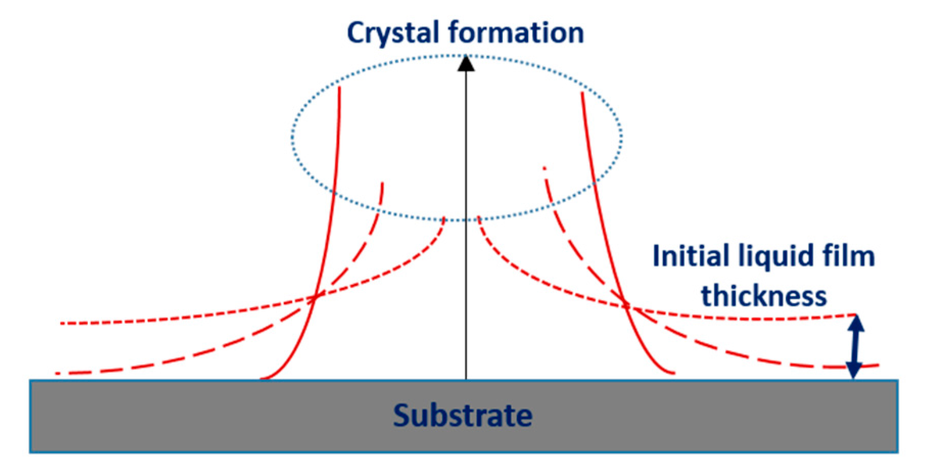
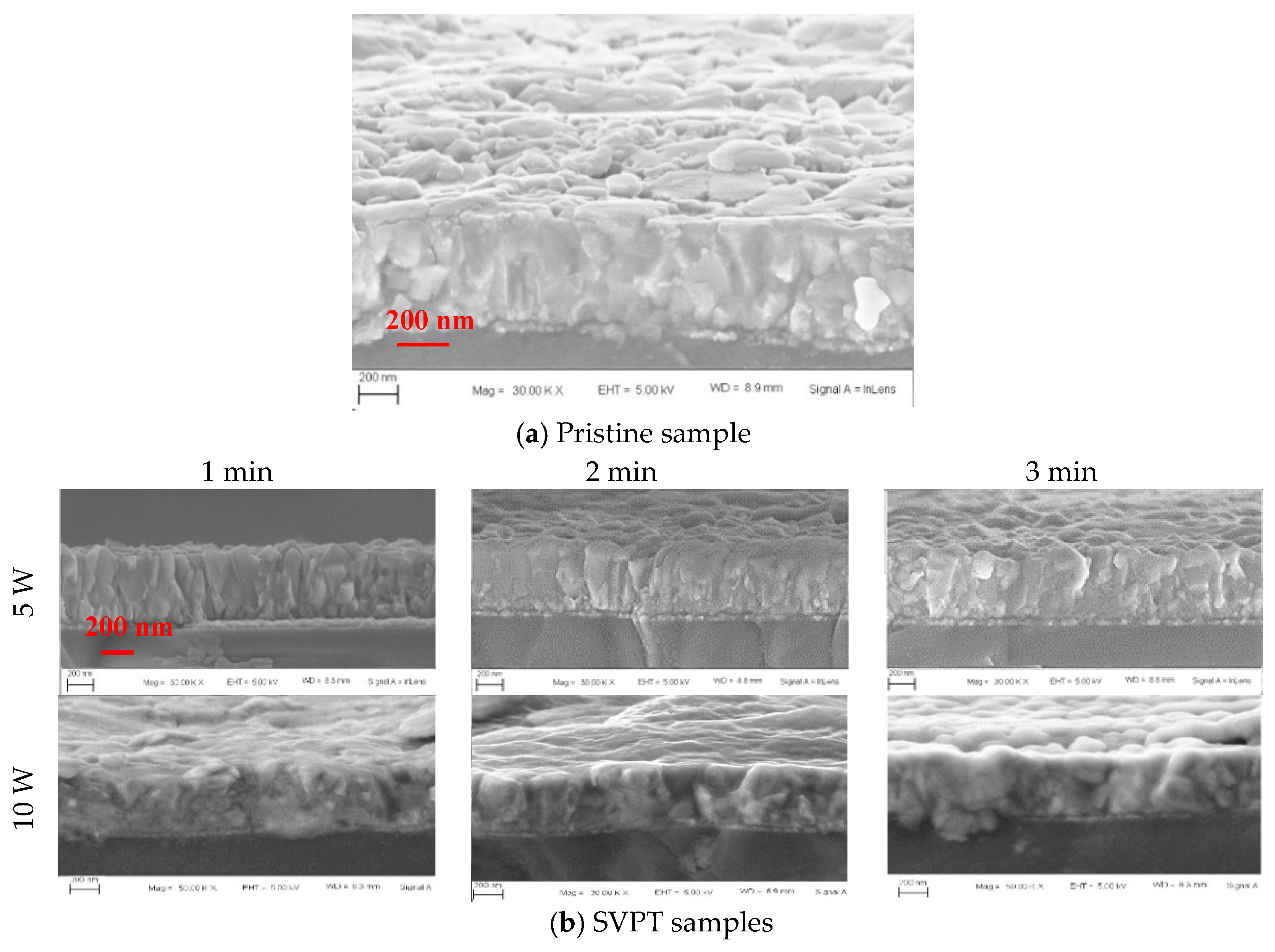
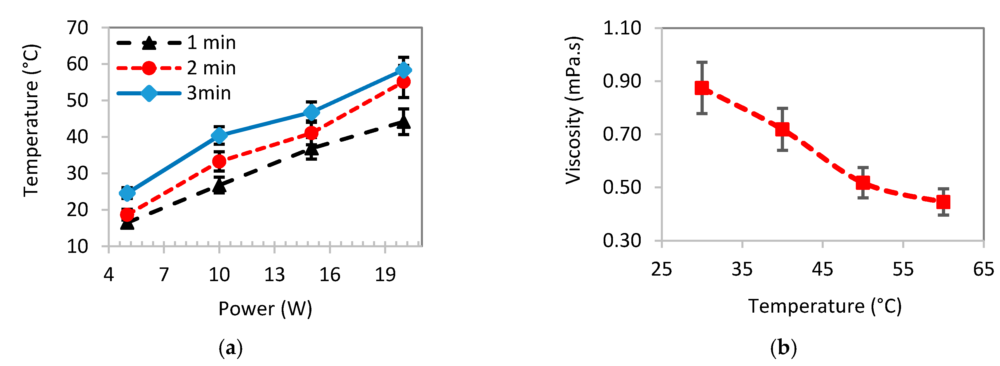
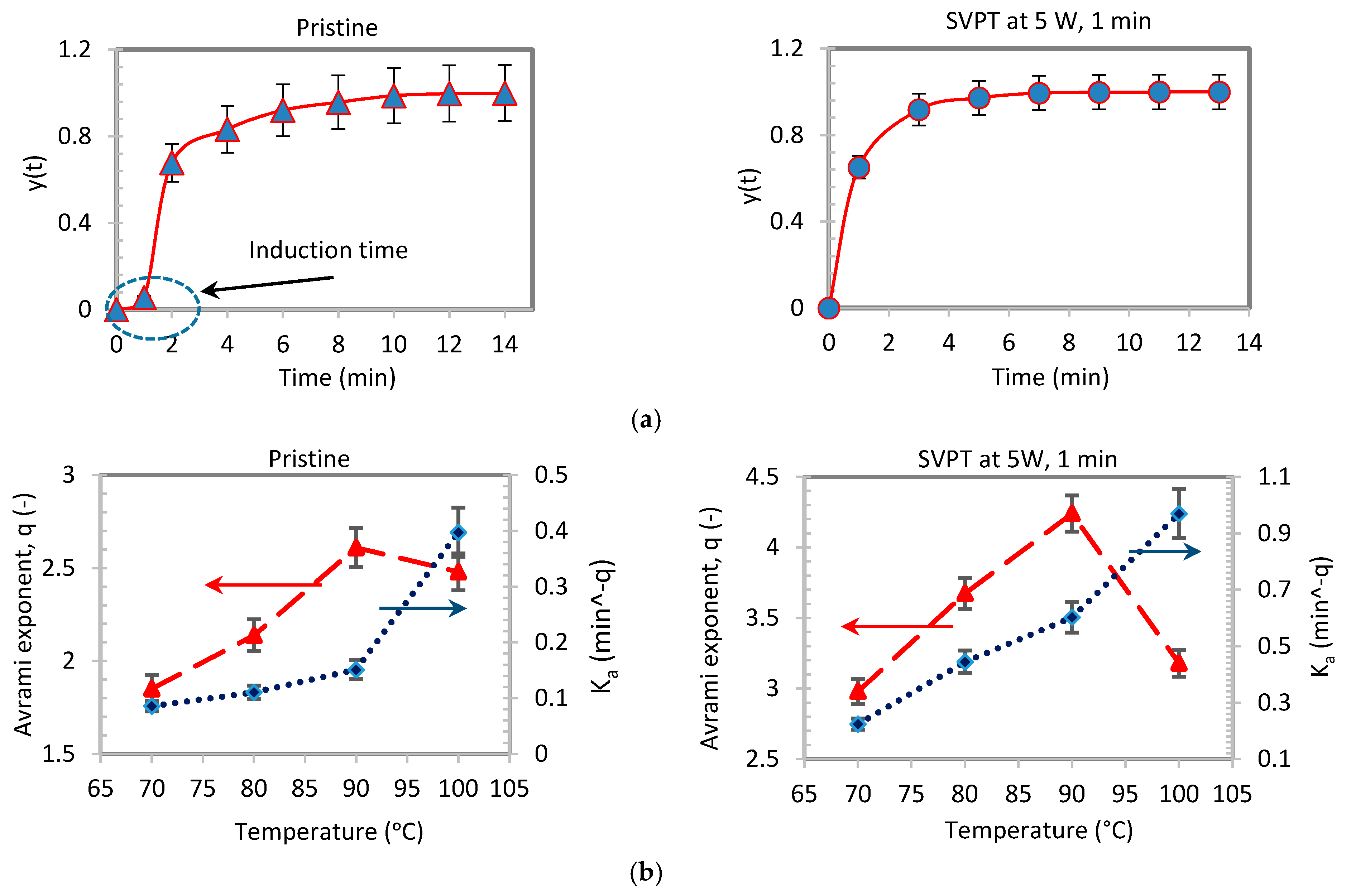
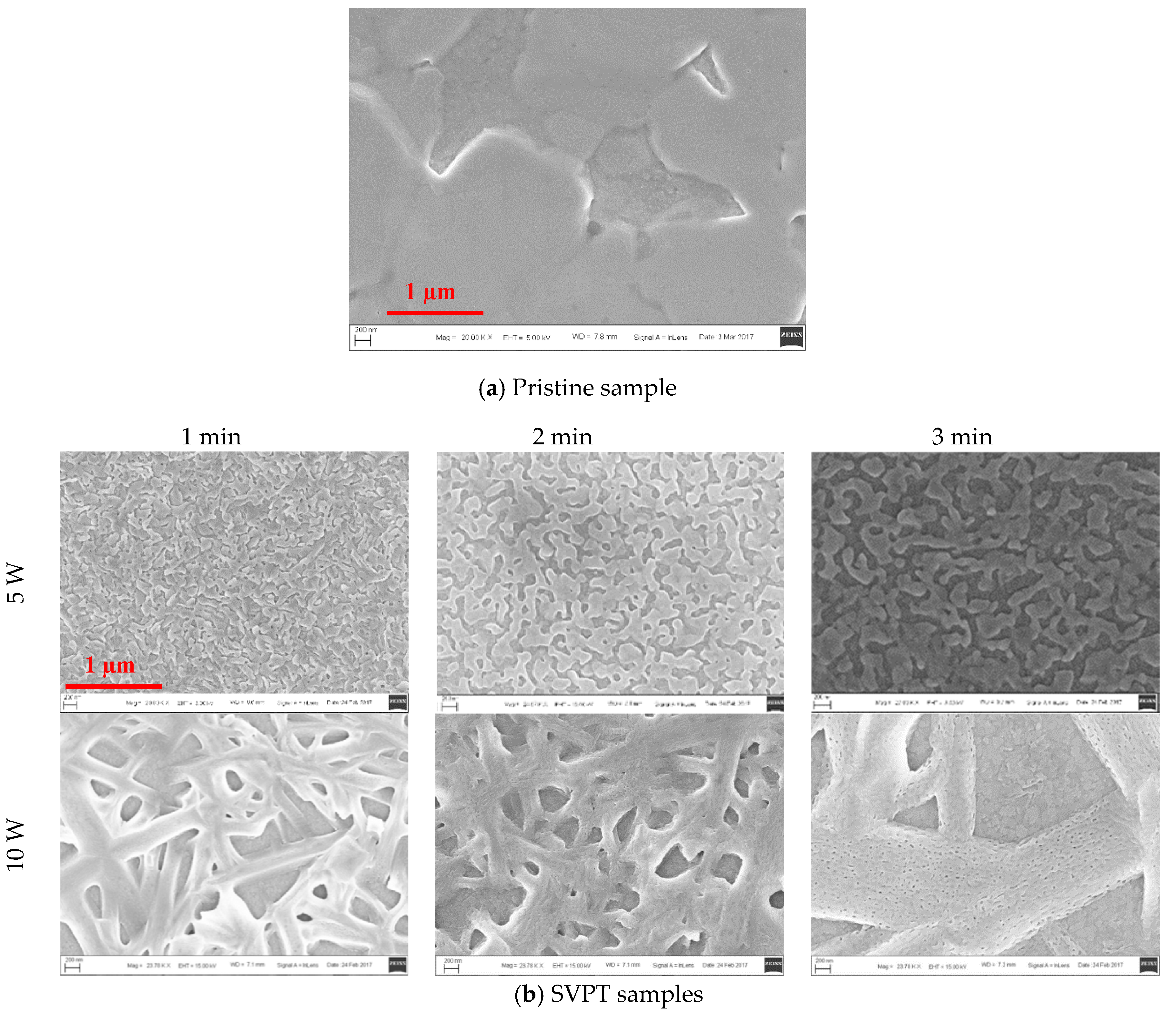
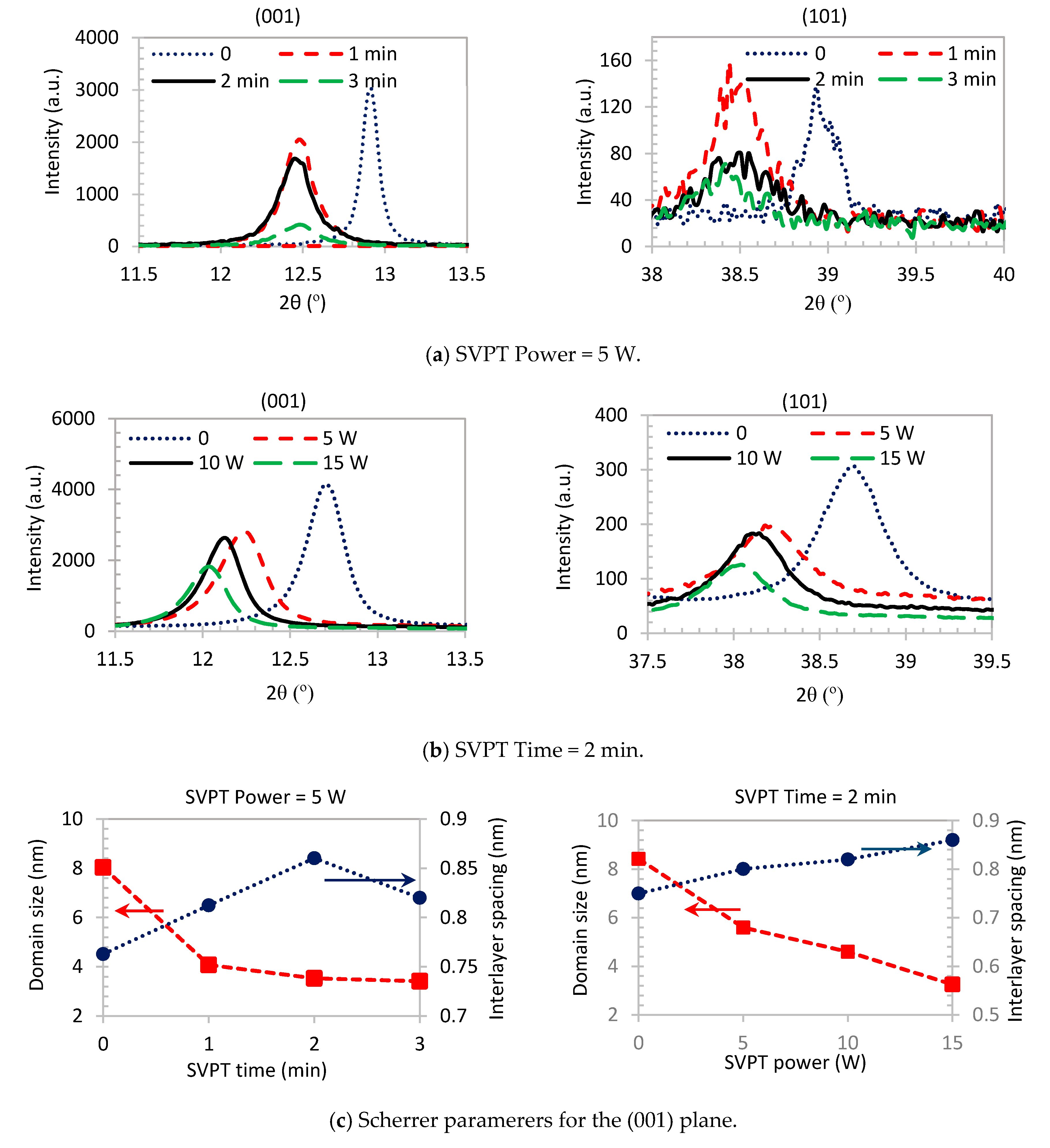
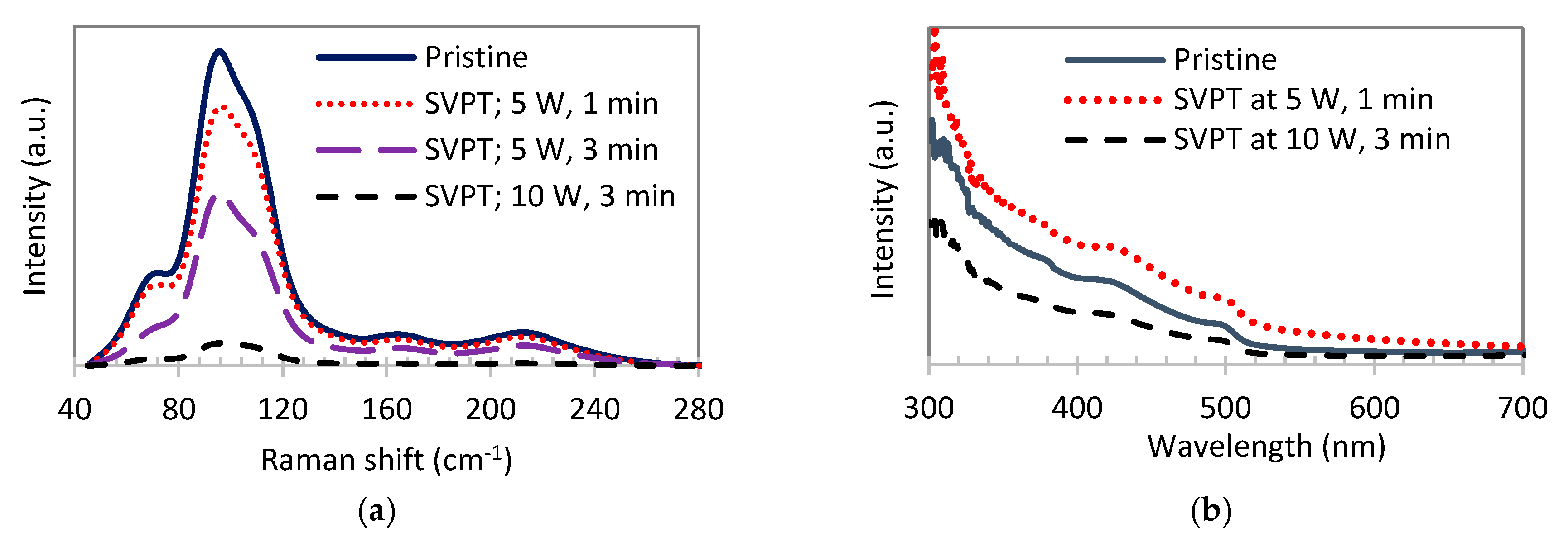
3. Results and Discussion

Figure 2 depicts the evolution of the morphology, configuration, and dispersion of PbI2 grains and their thin films, prepared without and with the application of the ultrasonic substrate vibration post treatment (SVPT). In the SVPT method [37], the wet-spun film is placed on an ultrasonic transducer in order to mildly excite the wet film. Further details are provided in Section 2. The corresponding cross-sectional SEM images, shown in Figure 3, reveal additional information on the effect of the SVPT on the spatial direction of the crystal growth and the film thickness. Several conclusive observations are made based on Figure 2: The pristine sample contains large laterally grown crystals. The application of the SVPT results in a decrease in the grain size. At the vibration for 5 W and 1 min a significant improvement is observed in the uniform distribution of the small grains and suppression of the dewetting. Excessive power of the vibration results in the formation of large grains again, negating the positive effect of the SVPT. Figure 3 also reveals some concrete facts as follows: The grain height (film thickness) in all cases is comparable and is about 400 nm, showing that the difference in the film morphology under various conditions is related to the planar grain growth. It is also substantiated that the SVPT at 5 W and 1 min results in very orderly vertically-grown grains, while the vibration at an increased power of 10 W nullifies the positive effect of the vibration observed at 5 W for 1 min. Such effects are elaborated in the following sections.
Crystallization is associated with two successive, parallel, or even competitive phenomena of the nucleation and growth. The term “nucleation” refers to the formation of stable primary seeds of a critical size, including the time gap from the occurrence of surpersaturation to appearing detectable embryos. Here “seed” denotes the molecular-sized crystallites with perfect forms, but still in co-existence with the solution with no clear boundaries. “Growth”, on the other hand, refers to the diffusion and absorption of the molecules of the solute onto the surfaces of the existing nuclei, resulting in the cluster formation, cluster development, and aggregation. The nature of the solution, method of the deposition, the substrate roughness, and the properties of the solute greatly affect the crystallization mechanism in the molecular scale [42,43].
The pristine thin film (c.f. Figure 2a) demonstrates laterally (2D) overgrown PbI2 grains with dewetted areas. We noticed that this planar growth behavior is amplified at lower concentrations, perhaps due to the lower rate of nucleation. PbI2 has a planar stacking structure repeating itself along the c-axis, normal to the substrate [17,44]. These planes intrinsically tend to develop from the side faces, in order to balance the surface interactive forces [5,44]. At low solution concentrations, the nucleation rate is low and the grain fronts are less confined by the neighboring grain borders and, therefore, propagate until the complete depletion of the solute from the diffusion layer.
Applying the SVPT at 5 W results in a major change in the film morphology, as seen in Figure 2b, where smaller grains are formed with distinct grain boundaries compared to the pristine film. By increasing the power of the vibration from 5 to 10 W, the morphology of thin film changes from irregular and small grains to grid-style large grain structures; thus, the SVPT is most effective at 5 W applied for 1 min. It is deduced that, as a result of the excitation by the ultrasonic vibration, the growth of large planar or 2D grains is suppressed due to an increase in the nucleation rate and the density of primary stable embryos [45,46,47]. In other words, in a dense population of stable seeds, the grain fronts will be confined by the neighboring cells. Hence, the role of the SVPT may be established as follows: in a regular spin-coating process, the rough surface of the substrate initiates heterogeneous nucleation, while the nucleation in the bulk solution occurs in a homogenous manner [48]. Such disharmony develops a bi-modal and non-uniform crystalline matrix. The SVPT enhances the heterogeneous nucleation rate on the substrate surface by supplying the energy of the nucleation [49] in two ways: Firstly, the vibrating substrate, regardless of its surface profile, transfers the vibrational energy to the bulk liquid. Secondly, the surface profile of the substrate (sputtered ITO film, in this case, with a roughness of ~5 nm) may have a role, as well, in that the atoms located at the peaks of the surface profile may reach higher temperatures than the average substrate temperature and, therefore, these hot spots may act as nucleation sites. From a thermodynamic point of view, the SVPT increases the evaporation rate [26] and the local temperature leading to a shift from the equilibrium state to the supersaturation point, which is the onset of nucleation. As a result of the aforementioned effects, the nucleation rate increases, while the critical size of the nuclei decreases [1]; therefore, more seeds will have the chance to reach the maturation limit and survive. Imposing ultrasonic vibration also creates microstreaming and micromixing motion within the film [27]. This results in uniform mixing and distribution of the embryos generated on the substrate surface and within the film. This uniform and accelerated nucleation favors the size distribution, compactness, dimensionality, and the morphology of the crystallites [1,46,47].
In addition to promoting the nucleation rate, the SVPT affects the crystal growth. Upon nucleation in both heterogeneous and homogenous modes, the clusters of solute molecules emerge and develop by absorbing more solute molecules from the solution. Under the SVPT, the growing clusters frequently collide with one another, due to the large density of nuclei and the excitement of the solution by the imparted energy and induced microstreaming. As a result, it is speculated that the rate of the PbI2 cluster breakup increases, relatively, resulting in the formation of smaller crystallites and the suppression of the crystallization dewetting, as observed in Figure 2b for the 5 W vibration power. While the SVPT with proper power and duration (5 W for 1 min) has a positive effect on the film morphology by decreasing the grain size and suppression of the crystallization dewetting, Figure 2b shows the adverse effect of prolonged duration and excessive power of the vibration on the grains and the film morphology, in that increasing the vibration time and power results in an increase in the grain size and the extent of the crystallization dewetting.
Figure 4 depicts the time variation of the temperature of the vibrated substrate, an ITO-coated glass, measured by an infrared thermometer, as well as the variation of the solution viscosity with temperature. The substrate temperature increases with both the power and time of vibration, and the solution viscosity decreases with the solution temperature, which is assumed to be in thermal equilibrium with the substrate due to the small thickness of the film and the mixing effect of vibration. Using these data one may be able to interpret the effect of the vibration time and power on the crystallization as follows: Compared to 5 W, the vibration power of 10 W imparts more energy and heat and produces stronger microstreaming. The increase of temperature shifts the thermodynamic equilibrium of solution to a higher solubility and, consequently, a higher supersaturation point. Thus, an excessive increase in temperature (due to a higher power or prolonged vibration) may result in dissolution of some formed embryos, which may be consumed to overgrow stable seeds. Moreover, in the reduced viscosity condition as a result of the increased temperature, the microstreaming effects will be more intensive [49,50], leading to a decrease in the effective rate of nucleation, negating the positive effect of the SVPT discussed above, causing the grains to overgrow and aggregate, as observed in Figure 2b. In general, one may speculate that the prolonged time and high power of vibration both have similar effects, i.e., both result in larger grain size, as seen in SEM images, and increased dewetting, although some differences are also observed, presumably due to stronger microstreaming and shear forces created when the vibration power is high. In general, the imposed vibration affects the crystal nucleation and growth, through both the fluid flow and thermodynamic states of the solution.
SEM images of Figure 2 and Figure 3 reveal that the chance of crystallization dewetting in a thin film depends on the size, morphology, density, dimensionality, and orientation of the crystals, and can be controlled to some extent by applying the SVPT. It was particularly argued that with ultrasonication the crystallization path can be altered to a nucleation-dominant regime. Herein, we attempt to verify this hypothesis from the kinetics perspective. The Kolmogorov-Johnson-Mehl-Avrami (KJMA) model, often referred to as the Avrami equation [51,52,53,54,55] governs the crystallization kinetics of each crystal as follows:
y ( t ) = 1 exp ( K a t q )
where Ka is the constant of crystallization rate and q is the Avrami exponent, which indicates the dimensionality and nucleation state, and y(t) is the time-dependent mass fraction of the crystallized phase, PbI2 in this work. It is more practical to evaluate y(t) by correlating it with the evaporated mass of the solvent through the following equation:
y ( t ) = W e ( t ) x s W i
where We(t) and Wi denote the total mass of the evaporated solvent at time t and the initial mass of the thin liquid film, respectively, and xs denotes the initial mass fraction of the solvent in the solution. Thermal gravimetry (TG) measurements of the pristine sample and the sample subjected to the SVPT at 5 W for 1 min were performed to calculate y(t) using Equation (2). For each sample four sets of the TG measurements were performed at 70, 80, 90, and 100 °C, where the mass of the thin film was measured every 2 min. The TG data (y(t) versus t) were then imported to MATLAB to calculate the Ka and q values based on Equation (1) via the least-square non-linear curve fitting (R2 = 0.995). The representative TG data, i.e., y(t) versus time corresponding to 90 °C is illustrated in Figure 5a. Figure 5b displays the q and Ka values versus temperature for the pristine sample and the sample subjected to the SVPT.
The values of the reaction rates (Ka) calculated from the TG measurements were plotted versus 1/RT in the log-log axes based of the Arrhenius equation, as follows:
K a = Z 0 exp ( E a R T )
Based on the aforementioned procedure, the nucleation frequency factor (Z0) and the activation energy of crystallization (Ea) of the pristine and the SVPT samples were obtained and listed in Table 1. The average Avrami constant and exponent, K ¯ a and q ¯ , obtained from the TG measurements, are also listed in Table 1. Z0 is interpreted as the number of attempts made by the nuclei in the unit of time to overcome the barrier energy [42,43]. Z0 also represents the induction time of recognizable seed formation [2,45]. Figure 5a shows that the time dependent crystallization of the pristine sample is associated with a small slope within the first 1 min, whereas in the SVPT sample, the crystallization shows a steep slope from the beginning, implying a fast rate from the early stages. Particularly, Figure 5a shows that within the first 1 min of the SVPT, a significant fraction of the crystals (>60%) have already emerged, due to the increased nucleation rate, as discussed before, demonstrating the merit of the SVPT.
The relatively lower activation energy of crystallization of the SVPT sample is consistent with the accelerated seeding or nucleation rate and reduced critical size of the stable nuclei, as observed in the previous section. The constant (Ka) of the SVPT sample is four times larger than that of the pristine sample, reflecting a shorter time required for crystal maturation in the former sample. The Avrami exponent power, q = q1 + q2, includes two factors: the crystal dimensionality (q1) and crystallization mode (q2). Table 1 shows that the Avarmi exponent of the SVPT sample is larger than that of the pristine sample. According to the literature, q1 is expected to be in the range of 1 to 3, where ~1 usually represents the formation of the rode-like 1D structures, ~2 is associated with the formation of planar or disc-like 2D structures or lateral growth, and ~3 is associated with the spatially-expanded or 3D columnar crystals [43,44,45,46,47]. The value of q2 which is typically in the range of 0 to 1 indicates the contribution of nucleation in the crystallization process. A larger q2 (→1) indicates a larger contribution of nucleation in the crystallization process [2,56,57,58,59]. Here, the average collective value of the Avrami exponent, i.e., q ¯ , is 2.27 for the pristine sample and 3.52 for the SVPT sample. From the increased q ¯ , we infer that the SVPT process not only can increase the rate (dominance) of nucleation, but also facilities multi-dimensional growth of the crystallites (transformation of the 2D grains to 3D grains), as the SEM images show.
In the next step, we utilized XRD to further investigate the effect of the ultrasonic vibration on the crystal lattice. Figure 6a,b (effect of the vibration time at 5 W) and (effect of the vibration power for 2 min of vibration) compare the XRD patterns of the PbI2 thin films for 2 θ angles at 12.93° and 38.95° associated with the (001) and (101) planes of hexagonal PbI2 crystals [14,44]. Figure 6c shows the variation of the domain size (L) and interlayer spacing (d) for the (001) plane, obtained using the following equations [17,60,61,62]:
L = n λ w C o s θ
d = n λ 2 s i n θ
where w is the full width of half maximum (FWHM) of the generic peak, θ denotes the angle of incidence, and n is the Scherrer constant, an integer referring to the order of diffraction, which is ~0.9 for spherical crystallites. λ indicates the wavelength which is constant and its value is 1.5406 Å [17,61,62]. Here, we approximated the crystallite shapes as rectangular; therefore, the Scherrer constant was corrected by multiplying it by 1.3. The effect of the lattice strain on the evolution of the FWHM and peak broadening was calculated by the Williamson-Hall method [63,64] and was found to be negligible. Therefore, Equation (4) was assumed to be adequate for the estimation of the domain size.
Figure 6 shows that on both (001) and (101) planes (parallel and normal to the substrate, respectively), vibration results in peak broadening and therefore a decrease in the domain size. Peak broadening is also interpreted as the increase of dimensionality, corroborating the results of the crystallization kinetics section. Additionally, a symmetric peak broadening, as observed for the (001) plane, indicates that all crystallites monotonically respond to the vibration [62,65,66]. The noise associated with the sporadic patterns of the (101) peak, particularly in Figure 6a, reflects the micro-strains between planes and plane displacement due to atomic imperfections, such as vacancies [60,61]. Peak intensity is another attribute of the XRD patterns. Overall, the peak intensity decreases in most samples subjected to the SVPT. Change of intensity may be due to a change in the atomic position and related imperfections in the crystalline array [60,61], which might have been induced by mechanical stresses and micro-strains caused by the SVPT. Figure 6 also shows a systematic peak shifting to the smaller Bragg angles as a result of the SVPT. This is a signature of the increased density of grain boundaries, which is consistent with a decrease in the domain size [66], as observed in Figure 6c. In addition, peak shifting toward the smaller or larger angles is due to a decreased or increased interlayer spacing, respectively [10,61,62], consistent with our results. As mentioned earlier, PbI2 crystals consist of I-Pb-I sheets and the crystal domain is composed of the repeating of such PbI2 layers. The bonding within the Pb and I is largely ionic, but adjacent PbI2 layers are bonded with the weak van der Walls forces [14,15]. It is speculated that the vibration induces micro-strains that affect these interlayer bonds, resulting in an increase in the interlayer spacing along the c-axis, i.e., normal to the substrate [17], as shown in Figure 6c for the (001) plane.
Raman spectroscopy provides information on the nanostructure and bonding status based on the molecular and crystal lattice vibrations. According to Figure 7a, the calibrated intensity of the Raman peaks systematically changes with the applied SVPT, i.e., the peak intensity decreases with the time and power of the imposed vibration. For a crystalline material, a decrease in the intensity implies a decrease in the crystal size [67,68]. It also shows that the sample has undergone a notable reorientation [67]. Thus, the data of Raman spectroscopy are consistent with the XRD data showing a decrease in the size of domains with an increase in the power and duration of vibration. The intensity of Raman peaks may also decrease by increasing the lattice compactness [68], i.e., the density of the crystallites. This behavior is consistent with the abovementioned argument on the accelerated nucleation and increased density and compactness of the grains due to imposed ultrasonic vibration.
Figure 7b compares the UV-vis absorption spectra of the pristine and two other samples subjected to the SVPT at 5 W for 1 min and 10 W for 3 min. The film absorbance depends on the two parameters of the PbI2 crystal band gap and PbI2 film coverage. A sharp drop in the absorption spectra of all samples occurs at about 520 nm, consistent with the band gap of PbI2 (2.31 eV) [69], i.e., for larger wavelengths, the low energy photons cannot be absorbed. It is also observed that the mild vibration improves the absorption, whereas the intensive and long duration vibration deteriorates the absorption with respect to the pristine sample, given that only in the case of a mild and short duration vibration (5 W, 1 min), a high coverage film forms (Figure 2a).

4. Conclusions

In this work, the effect of imposing ultrasonic vibration on the substrate of a thin liquid film of PbI2 solution was studied on the PbI2 crystal growth and film morphology. It is concluded that while pristine crystals tend to overgrow in the planar direction ((001) plane), when the wet film is excited by a mild ultrasonic vibration (40 kHz, 5 W) for the optimum time of 1 min, the activation energy of crystallization decreases and the nucleation rate increases, leading to the confinement of the excessive crystal growth in the planar direction, and organized crystal growth normal to the substrate, creating 3D columnar structures. As a result, the film morphology significantly improves, owing to the epitaxial growth of compact 3D grains and the suppression of the crystallization dewetting. The XRD results showed a Bragg shift in major peaks and peak broadening, as a result of the imposed ultrasonic vibration. The absorption of the film excited by the ultrasonic vibration at the optimum condition was also increased. It is concluded that the post or in situ treatment of the solution-processed PbI2 thin films on ITO substrate could result in a well-controlled crystallization (similar to epitaxial growth in vapor deposition) and the preparation of a defect-free PbI2 thin film, which has several applications in emerging thin film devices, such as sensors and perovskite solar cells.

Acknowledgments

Financial support from the Shanghai Municipal Education Commission via the Oriental Scholar fund and the funding form the National Natural Science Foundation of China (NSFC) is acknowledged.

Author Contributions

F.Z. and M.E. conceived the idea. F.Z. designed and performed the experiments and analyzed the data. F.Z. and M.E. wrote the paper and approved the final version of the paper.

Conflicts of Interest

The authors declare no conflict of interest.

References

  1. Christo, N.N.; Hodzhaoglu, F.V.; Ivaylo, L.D. Kinetics of insulin crystal nucleation, energy barrier, and nucleus size. Cryst. Growth Des. 2011, 11, 196–202. [Google Scholar] [CrossRef]
  2. Ihli, J.; Wong, W.C.; Noel, E.H.; Kim, Y.Y.; Kulak, A.N.; Christenson, H.K.; Duer, M.J.; Meldrum, F.C. Dehydration and crystallization of amorphous calcium carbonate in solution and in air. Nat. Commun. 2014, 5, 3169. [Google Scholar] [CrossRef] [PubMed]
  3. Hill, J.C.; Koza, J.A.; Switzer, J.A. Eectrodeposition of epitaxial lead-iodide and conversion to textured methylammonium lead iodide perovskite. ACS App. Mater. Interfaces 2015, 7, 26012–26016. [Google Scholar] [CrossRef] [PubMed]
  4. Wang, Y.; Sun, Y.Y.; Zhang, S.; Lu, T.M.; Shi, J. Band gap engineering of a soft inorganic compound PbI2 by incommensurate van der Waals epitaxy. App. Phys. Lett. 2016, 108, 013105. [Google Scholar] [CrossRef]
  5. Zhu, X.; Sun, H.; Yang, D. Fabrication and characterization of X-ray array detector based on polycrystalline PbI2 thick films. J. Mat. Sci. Mat. Electron. 2014, 25, 3337–3343. [Google Scholar] [CrossRef]
  6. Ying, C.; Shi, C.; Wu, N.; Zhang, J.; Wang, M. Two-layer structured PbI2 thin film for efficient planar perovskite solar cells. Nanoscale 2015, 7, 12092. [Google Scholar] [CrossRef] [PubMed]
  7. Zhang, Z.; Sun, D.W.; Zhu, Z.; Cheng, L. Enhancement of crystallization processes by power ultrasound: Current state-of-the-art. Compr. Rev. Food Sci. Food Saf. Res. Adv. 2015, 14, 303–316. [Google Scholar] [CrossRef]
  8. Cao, J.; Wang, F.; Yu, H.; Zhou, Y.; Lu, H.; Zhao, N.; Wong, C.P. Porous films for the fabrication of efficient, stable perovskite solar cells via sequential deposition. J. Mater. Chem. A 2016, 4, 10223–10230. [Google Scholar] [CrossRef]
  9. Acuna, D.; Krishna, B.; Shaji, S.; Sepolveda, S.; Menchaca, J.L. Growth and properties of lead iodide thin films by spin coating. Bull. Mater. Sci. 2016, 39, 1453–1460. [Google Scholar] [CrossRef]
  10. Zhang, J.; Song, T.; Zhang, Z.; Ding, K.; Huang, F.; Sun, B. Layered ultrathin PbI2 single crystals for high sensitivity flexible photodetectors. J. Mater. Chem. C 2015, 3, 4402–4406. [Google Scholar] [CrossRef]
  11. Habibi, M.; Zabihi, F.; Ahmadian-Yazdi, M.R.; Eslamian, M. Progress in emerging solution-processed thin film solar cells—Part II: Perovskite solar cells. Renew. Sustain. Energy Rev. 2016, 62, 1012–1031. [Google Scholar] [CrossRef]
  12. Xiong, H.; DeLucab, D.; Ruic, Y.; Li, Y.; Reichmanis, E.; Zhang, Q.; Wang, H. Solvent vapor annealing of oriented PbI2 films for improved crystallization of perovskite films in the air. Sol. Energy Mater. Sol. Cells 2017, 166, 167–175. [Google Scholar] [CrossRef]
  13. Zhang, T.; Yang, M.; Zhao, Y.; Zhu, K. Controllable sequential deposition of planar CH₃NH₃PbI₃ perovskite films via adjustable volume expansion. Nano Lett. 2015, 15, 3959–3963. [Google Scholar] [CrossRef] [PubMed]
  14. Kariper, A. Optical and structural properties of PbI2 thin film produced via chemical dipping method. Opt. Rev. 2016, 23, 401–408. [Google Scholar] [CrossRef]
  15. Chaudhary, S.K. Lead iodide crystals as input material for radiation detectors. Cryst. Struct. Theory Appl. (CSTA) 2012, 1, 21–24. [Google Scholar] [CrossRef]
  16. Eslamian, M. Inorganic and organic solution-processed thin film devices. Nano-Micro Lett. 2017, 9, 3. [Google Scholar] [CrossRef]
  17. Mousa, A.M.; Al-rubaie, N.J. The influence of deposition conditions on structural properties of PbI2. Texture Stress Microstruct. 2009, 494537. [Google Scholar] [CrossRef]
  18. Matuchov, M.; Zdansky, K.; Zavdil, J.; Tonn, J.; Mousa, M.; Jafar, A.-G.; Danilewsky, A.N.; Croll, A.; Maixner, J. Influence of doping and non-stoichiometry on the quality of lead iodide for use in X-Ray detection. J. Cryst. Growth 2010, 312, 1233–1239. [Google Scholar] [CrossRef]
  19. Habibi, M.; Rahimzadeh, A.; Eslamian, M. On dewetting of thin films due to crystallization (crystallization dewetting). Eur. Phys. J. E 2016, 39, 30. [Google Scholar] [CrossRef] [PubMed]
  20. Okerberg, B.C.; Berry, B.C.; Garvey, T.R.; Douglas, J.F.; Karim, A.; Soles, C.L. Competition between crystallization and dewetting fronts in tin polymer films. Soft Matter 2009, 5, 562–567. [Google Scholar] [CrossRef]
  21. Peron, N.; Brochard-Wyart, F.; Duval, H. Dewetting of low-viscosity films at solid/liquid interfaces. Langmuir 2012, 28, 15844–15852. [Google Scholar] [CrossRef] [PubMed]
  22. Zabihi, F.; Xie, Y.; Gao, S.; Eslamian, M. Morphology, conductivity and wetting characteristics of PEDOT:PSS thin films deposited by spin and spray coating. Appl. Surf. Sci. 2015, 338, 163–177. [Google Scholar] [CrossRef]
  23. Shklyaev, S.; Khenner, M.; Alabuzhev, A.A. Enhanced stability of a dewetting thin liquid film in a single-frequency vibration field. Phys. Rev. E 2008, 77, 036320. [Google Scholar] [CrossRef] [PubMed]
  24. Benilov, E.S.; Chugunova, M. Waves in liquid films on vibrating substrates. Phys. Rev. E 2010, 81, 036302. [Google Scholar] [CrossRef] [PubMed]
  25. Rahimzadeh, A.; Eslamian, M. Stability of thin liquid films subjected to ultrasonic vibration and characteristics of the resulting thin solid films. Chem. Eng. Sci. 2017, 158, 587–598. [Google Scholar] [CrossRef]
  26. Rahimzadeh, A.; Eslamian, M. On evaporation of thin liquid films subjected to ultrasonic substrate vibration. Int. Commun. Heat Mass Transf. 2017, 83, 15–22. [Google Scholar] [CrossRef]
  27. Eslamian, M. Excitation by acoustic vibration as an effective tool for improving the characteristics of the solution-processed coatings and thin films. Prog. Org. Coat. 2017, 113, 60–73. [Google Scholar] [CrossRef]
  28. Hem, S.L. The effect of ultrasonic vibration on crystallization processes. Ultrasonics 1967, 5, 202–207. [Google Scholar] [CrossRef]
  29. Djordjevic, S.; Poinern, G.E.J.; Brundavanam, R.K.; Fawcett, D.; Nikoloski, A.; Prokic, M. Enhanced deposition and reflective properties of thin aluminum films by substrate vibration. Int. J. Sci. 2014, 3, 67–73. [Google Scholar]
  30. Ruirun, C.; Zheng, D.; Tengfei, M.; Hongsheng, D.; Yanqing, S.; Jingjie, G.; Hengzhi, F. Effects of ultrasonic vibration on the microstructure and mechanical properties of high alloying TiAl. Sci. Rep. 2017, 7, 41463. [Google Scholar] [CrossRef] [PubMed]
  31. Nahidul Islam, M.; Zhang, M.; Adhikari, B. Ultrasound-assisted freezing of fruits and vegetables: Design, development, and applications. Glob. Food Secur. Wellness 2017, 457–487. [Google Scholar] [CrossRef]
  32. Gielen, B.; Jordens, J.; Thomassen, L.C.J.; Braeken, L.; Gerven, T.V. Agglomeration control during ultrasonic crystallization of an active pharmaceutical ingredient. Crystals 2017, 7, 40. [Google Scholar] [CrossRef]
  33. Choi, J.Y.; Kim, K.J.; Yoo, J.B.; Kim, D. Properties of cadmium sulfide thin films deposited by chemical bath deposition with ultrasonication. Sol. Energy 1998, 64, 41–47. [Google Scholar] [CrossRef]
  34. Diemer, P.J.; Lyle, C.R.; Mei, Y.; Sutton, C.; Payne, M.M.; Anthony, J.E.; Coropceanu, V.; Bredas, J.L.; Jurchescu, O.D. Vibration-assisted crystallization improves organic/dielectric interface in organic thin-film transistors. Adv. Mater. 2013, 25, 6956–6962. [Google Scholar] [CrossRef] [PubMed]
  35. Zabihi, F.; Ahmadian-Yazdi, M.R.; Eslamian, M. Photocatalytic Graphene-TiO2 thin films fabricated by low-temperature ultrasonic vibration-assisted spin and spray coating in a sol-gel process. Catalysts 2017, 7, 136. [Google Scholar] [CrossRef]
  36. Zabihi, F.; Eslamian, M. Substrate vibration-assisted spray coating (SVASC): Significant improvement in nano-structure, uniformity, and conductivity of PEDOT:PSS thin films for organic solar cells. J. Coat. Technol. Res. 2015, 12, 711–719. [Google Scholar] [CrossRef]
  37. Wang, Q.; Eslamian, M. Improving uniformity and nanostructure of solution-processed thin films using ultrasonic substrate vibration post treatment (SVPT). Ultrasonics 2016, 67, 55–64. [Google Scholar] [CrossRef] [PubMed]
  38. Zabihi, F.; Chen, Q.; Xie, Y.; Eslamian, M. Fabrication of efficient graphene-doped polymer/fullerene bilayer organic solar cells in air using spin coating followed by ultrasonic vibration post treatment. Superlattices Microstruct. 2016, 100, 1177–1192. [Google Scholar] [CrossRef]
  39. Zabihi, F.; Ahmadian-Yazdi, M.R.; Eslamian, M. Fundamental study on the fabrication of inverted planar perovskite solar cells using two-step sequential substrate vibration-assisted spray coating (2S-SVASC). Nanoscale Res. Lett. 2016, 11, 71. [Google Scholar] [CrossRef] [PubMed]
  40. Eslamian, M.; Zabihi, F. Ultrasonic substrate vibration-assisted drop casting (SVADC) for the fabrication of solar cell arrays and thin film devices. Nanoscale Res. Lett. 2015, 10, 462. [Google Scholar] [CrossRef] [PubMed]
  41. Ahmadian-Yazdi, M.R.; Eslamian, M. Toward scale-up of perovskite solar cells: Annealing-free perovskite layer by low-cost ultrasonic substrate vibration of wet films. Mater. Today Commun. 2018, 14, 151–159. [Google Scholar] [CrossRef]
  42. Asha, K.S.; Kavyasree, P.R.; George, A.; Mandal, S. The role of solvents in framework dimensionality and their effect on band gap energy. Dalton Trans. 2015, 44, 1009–1016. [Google Scholar] [CrossRef] [PubMed]
  43. Birnie, P.; Dunbar, A. Model for drying control co-solvent selection for spin coating uniformity: The thin film limit. Langmuir 2013, 29, 9072–9078. [Google Scholar] [CrossRef] [PubMed]
  44. Fu, F.; Kranz, L.; Yoon, S.; Lockinger, J.; Jager, T.; Perrenoud, J.; Feurer, T.; Gretener, C.; Bucheler, S.; Tiwari, A.N. Controlled growth of PbI2 nanoplates for rapid preparation of CH3NH3PbI3 in planar perovskite solar cells. Phys. Status Solids A 2015, 212, 2708–2717. [Google Scholar] [CrossRef]
  45. Sumari, S.; Roesyadi, A.; Sumarno, S. Effects of ultrasound on the morphology particle size, crystallinity and crystalline size of cellulose. Chem. Chem. Eng. Biotechnol. Food Ind. 2013, 14, 229–239. [Google Scholar]
  46. Wu, X.; Wang, Y.; Zhou, S.; Yuan, X.Y.; Gao, T.; Wang, K.; Lou, S.; Liu, Y.; Shi, X. Morphology control, crystal growth, and growth mechanism of hierarchical tellurium (Te) microstructures. Cryst. Growth Des. 2013, 13, 136–142. [Google Scholar] [CrossRef]
  47. Tidhar, Y.; Edri, E.; Weissman, H.; Zohar, D.; Hodes, G.; Cahen, D.; Rybtchinski, B.; Kirmayer, S. Crystallization of methyl ammonium lead halide perovskites: Implications for photovoltaic applications. J. Am. Chem. Soc. 2014, 136, 13249–13256. [Google Scholar] [CrossRef] [PubMed]
  48. Sander, J.R.G.; Zeiger, B.W.; Suslick, K.S. Sonocrystallization and sonofragmentation. Ultrason. Sonochem. 2014, 21, 1908–1915. [Google Scholar] [CrossRef] [PubMed]
  49. Caruso, M.M.; Davis, D.A.; Shen, Q.; Odom, S.A.; Sottos, N.R.; White, S.R.; Moore, J.S. Mechanically-induced chemical changes in polymeric materials. Chem. Rev. 2009, 109, 5755–5798. [Google Scholar] [CrossRef] [PubMed]
  50. Kolgomorov, A.N. A statistical theory for the recrystallization of metals. Izv. Akad. Nauk SSSR Ser. Mat. 1937, 3, 355–359. [Google Scholar]
  51. Johnson, W.A.; Meh, R.F. Reaction kinetics in processes of nucleation and growth. Trans. Metall. Soc. AIME 1939, 135, 416–458. [Google Scholar]
  52. Avrami, M. Kinetics of phase change, I. General Theory. J. Chem. Phys. 1939, 7, 1103–1112. [Google Scholar] [CrossRef]
  53. Avrami, M. Kinetics of phase change, II. General Theory. J. Chem. Phys. 1940, 8, 212. [Google Scholar] [CrossRef]
  54. Avrami, M. Kinetics of phase change, III. General Theory. J. Chem. Phys. 1941, 9, 177–181. [Google Scholar] [CrossRef]
  55. Kaswan, A.; Kumari, V.; Patidar, D.; Shai Saxena, N.; Sharma, K. Kinetics of crystallization of Ge30-xSe70Sbx (x = 15, 20, 25) chalcogenide glasses. Proc. Appl. Ceram. 2014, 8. [Google Scholar] [CrossRef]
  56. Linnikov, O.D. Relation between activation energy for nucleation and of growth of crystals. Nanosyst. Phys. Chem. Math. 2014, 5, 546–552. [Google Scholar]
  57. Miller, R.M.; Poulos, A.S.; Robles, E.S.J.; Brooks, N.J.; Ces, O.; Cabral, J.T. Isothermal crystallization kinetics of sodium dodecyl sulfate-water micellar solutions. Cryst. Growth Des. 2016, 16, 3379–3388. [Google Scholar] [CrossRef]
  58. Fidalgo-Marijuan, A.; Amayuelas, E.; Barandika, G.; Bazán, B.; Urtiaga, M.K.; Arriortua, M.I. Coordination and crystallization molecules: Their interactions affecting the dimensionality of metalloporphyrinic SCFs. Molecules 2015, 20, 6683–6699. [Google Scholar] [CrossRef] [PubMed]
  59. Lam, R.S.H.; Rogers, M.A. Experimental validation of the modified Avrami model for non-isothermal crystallization, conditions. Cryst. Eng. Commun. 2011, 13, 866–875. [Google Scholar] [CrossRef]
  60. Muhammed Shafi, P.; Chandra Bose, A. Impact of crystalline defects and size on X-ray line broadening: A phenomenological approach for tetragonal SnO2 nanocrystals. AIP Adv. 2015, 5, 057137. [Google Scholar] [CrossRef]
  61. Monshi, A.; Foroughi, M.R.; Monshi, M.R. Modified Scherrer equation to estimate more accurately nano-crystallite size using XRD. World J. Nano Sci. Eng. 2012, 2, 154–160. [Google Scholar] [CrossRef]
  62. Bushroa, A.R.; Rahbari, R.G.; Masjuki, H.H.; Muhamad, M.R. Approximation of crystallite size and microstrain via XRD line broadening analysis in TiSiN thin films. Vacuum 2012, 86, 1107–1112. [Google Scholar] [CrossRef]
  63. Halder, N.C.; Wagner, C.N.J. Separation of particle size and lattice strain in integral breadth measurements. Acta Crystallogr. 1966, 20, 312–313. [Google Scholar] [CrossRef]
  64. Taraka Prabhu, Y.; Venkateswara Rao, K.; Sai Kumar, V.-S.; Siva Kumari, B. X-Ray analysis by williamson-hall and size-strain plot methods of ZnO nanoparticles with fuel variation. World J. Nano Sci. Eng. (WJNSE) 2014, 4, 21–28. [Google Scholar] [CrossRef]
  65. Zhao, Y.; Zhang, J. Microstrain and grain-size analysis from diffraction peak width and graphical derivation of high pressure thermomechanics. J. Appl. Cryst. 2008, 41, 1095–1108. [Google Scholar] [CrossRef]
  66. Groma, I.; Monnet, G. Analysis of asymmetric broadening of X-ray diffraction peak profiles caused by randomly distributed polarized dislocation dipoles and dislocation walls. J. Appl. Crystallogr. 2002, 35, 589–593. [Google Scholar] [CrossRef]
  67. Choquette, S.J.; Etz, E.S.; Hurst, W.S.; Blackburn, D.H.; Leigh, S.D. Relative intensity correction of Raman spectrometers: NIST SRMs 2241 through 2243 for 785 nm, 532 nm, 488 nm/514.5 nm excitation. Appl. Spectrosc. 2007, 61, 117–129. [Google Scholar] [CrossRef] [PubMed]
  68. Colomban, P.; Slodczyk, A. Raman Intensity: An important tool in the study of nanomaterials and nanostructures. Acta Phys. Pol. A 2009, 116. [Google Scholar] [CrossRef]
  69. Ahlawat, D.S. Study of band gap energy and thermal properties of PbI2 by photoacoustic spectroscopy. Mod. Phys. Lett. B 2012, 26, 1250098. [Google Scholar] [CrossRef]
Figure 1. Schematic of the emergence of a crystal from a liquid film with time, causing possible dewetting adjacent to a protruded crystal (crystallization dewetting).
Crystals 08 00060 g001
Figure 2. Top-view SEM images showing the evolution of the crystal morphology by the ultrasonic vibration time and power. (a) Pristine sample and (b) samples subjected to the SVPT at varying times and powers. All images have the same magnification and scale bar.
Crystals 08 00060 g002
Figure 3. Cross-sectional SEM images of (a) pristine PbI2 thin films and (b) thin films subjected to the SVPT. All images have the same magnification and scale bar.
Crystals 08 00060 g003
Figure 4. (a) Thermal history of the ultrasonically vibrated substrate (ITO-coated glass), and (b) variation of the viscosity of PbI2-DMF solution (0.5 M) as a function of temperature. The error bars represent the standard deviation.
Crystals 08 00060 g004
Figure 5. (a) Crystallized fraction, y(t), versus time, t, measured by TG at 90 °C. (b) Avrami exponent and the rate constant versus temperature, for pristine and the SVPT thin films (5 W and 1 min).
Crystals 08 00060 g005
Figure 6. Effect of the SVPT on XRD peaks of the PbI2 thin films. (a) Effect of the vibration time at a fixed vibration power of 5 W; (b) the effect of the vibration power on samples subjected to a 2 min SVPT; and (c) crystal domain size and interlayer spacing of two samples; the left diagram shows the samples prepared at varying vibration time at a constant power of 5 W, and the right diagram shows the samples prepared at varying ultrasonic power applied for 2 min.
Crystals 08 00060 g006
Figure 7. (a) Raman spectra and (b) UV-vis absorption spectra of the pristine sample and the samples subjected to the SVPT.
Crystals 08 00060 g007
Table 1. Crystallization kinetics parameters of pristine samples and the samples subjected to the SVPT at 5 W for 1 min, extracted from the TG data. K ¯   and   q ¯ are the average values obtained from four TG measurements at 70, 80, 90, and 100 °C.
Pristine SamplesSVPT Samples
q ¯ K ¯ a (min−q)Ea (kJ·mol−1)Z0 (min−q) q ¯ K ¯ a (min−q)Ea (kJ·mol−1)Z0 (min−q)
2.270.1552.463.20 × 1063.520.5645.719.82 × 106

