Abstract
In this work, molecular dynamics simulations of the nanoscratching of polycrystalline and singlecrystalline silicon substrates using a single-crystal diamond tool are conducted to investigate the grain size effect on the nanoscale wear process of polycrystalline silicon. We find that for a constant indentation depth, both the average normal force and friction force are much larger for single-crystalline silicon compared to polycrystalline silicon. It is also found that, for the polycrystalline substrates, both the average normal force and friction force increase with increasing grain size. However, the friction coefficient decreases with increasing grain size, and is the smallest for single-crystalline silicon. We also find that the quantity of wear atoms increases nonlinearly with the average normal load, inconsistent with Archard’s law. The quantity of wear atoms is smaller for polycrystalline substrates with a larger average grain size. The grain size effect in the nanoscale wear can be attributed to the fact that grain boundaries contribute to the plastic deformation of polycrystalline silicon.
1. Introduction
Silicon has been the material most commonly used in microelectromechanical systems (MEMS). However, high wear has been one of the major barriers to the development and commercialization of silicon-based MEMS [1,2,3]. Therefore, in the past decades, great efforts have been made to study the wear mechanisms of silicon. Most of the previous studies analyzed the wear process based on the classic Archard’s law [4], which describes the worn volume as proportional to both the applied load and the sliding distance. However, recent studies have shown that the nanoscale wear processes cannot be fully described by Archard’s wear law [5,6,7]. For example, the wear rate is typically not constant for the nanoscale wear of single-crystal silicon tips [5,6,7,8,9,10]. In particular, the recently proposed atom-by-atom wear mechanism was used to explain the wear of single-crystal silicon tips sliding on a polymer surface [5] and a diamond surface [7]. In addition, Alsem et al. studied the sliding wear mechanisms using polycrystalline silicon friction MEMS specimens [11,12]. Bhushan et al. carried out nanoscratching tests on silicon (100), specifically doped and undoped polysilicon at normal loads ranging from 20 to 100 µN [13,14]. They found that the scratch depth for silicon (100) was smaller than that for the undoped polysilicon. Chung et al. also performed experiments to evaluate the wear coefficients of silicon (100), silicon oxide, silicon nitride, and polysilicon under 100 µN normal load. They found that the average wear coefficient of silicon (100) was smaller than that of polysilicon [15].
In addition to experimental investigations, molecular dynamics (MD) simulations have also been used to explore the nanoscale deformation and wear mechanisms of silicon [16,17,18,19,20,21,22]. Zhang et al. found scratching induced amorphous phase transformation in single-crystal silicon [16]. Nanoscale abrasive wear on single-crystal silicon has been studied using large-scale MD [17]. In addition, MD simulations have been carried out to investigate the nanoscale cutting of single-crystal silicon, and amorphous phase transformation has been observed [18,19]. Chrobak et al. found that the plasticity of bulk silicon is dominated by phase transformations, whereas that of silicon nanoparticles is dislocation-driven [20]. Recently, Goel et al. found that phase transformation is the primary plastic deformation mechanism in the nanoindentation deformation process of polycrystalline silicon using MD simulation and experimentation [21]. Goel et al. also investigated the cutting process of polycrystalline silicon using MD [22].
Overall, so far, most of the studies in the literature have focused on the mechanical and wear behaviors of single-crystal silicon, although some work has been done to study the deformation and wear process of polycrystalline silicon [13,14,15,21,22]. In addition, it is well-known that grain refinement is a promising way of improving the friction- and wear-resistance of metals [23,24]. However, to our best knowledge, at present, a study that investigates how the grain size affects the friction and wear behaviors of polycrystalline silicon is still lacking, even though polycrystalline silicon is extensively used in most real-world applications (e.g., solar cell substrates). This study is intended to fill this gap. As MD simulation can capture atomic details of the wear process, MD simulation has been a powerful tool to study the mechanisms of nanoscale wear [25]. Therefore, in this work, MD simulations of the nanoscratching process of single-crystal and polycrystalline silicon using a diamond tool are performed to explore the effects of grain size on the wear behaviors of polycrystalline silicon.
2. Simulation Details
In this work, MD simulations were carried out using the large-scale atomic/molecular massively parallel simulator (LAMMPS) [26]. We analyzed the simulation results using OVITO [27]. The simulation model consisted of a hemispherical rigid single-crystal diamond tool and a silicon substrate (Figure 1). The hemispherical diamond tool created from perfect diamond atomic lattices had a radius of 5 nm. The single-crystal silicon substrate had the three crystal orientations of x-[100], y-[010], and z-[001]. The scratching was conducted on the (001) surface along the [−100] direction. To address the effect of grain size on the wear, polycrystalline silicon substrates with average grain size ranging from 2 to 5 nm were generated by Voronoi tessellation code [21,22,28]. Dimensions of single-crystalline silicon and polycrystalline silicon with different average grain sizes are listed in Table 1.
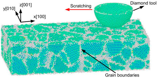
Figure 1.
Molecular dynamics (MD) simulation model of the wear of polycrystalline silicon.

Table 1.
Dimensions of single-crystalline silicon and polycrystalline silicon with different average grain sizes.
The silicon substrates were divided into three different areas: boundary atoms, thermostat atoms, and Newtonian atoms. Atoms in the bottom 0.5-nm region of substrate were kept fixed in space as boundary atoms. Atoms in the 1-nm-thick region of substrate adjacent to the boundary atoms were thermostat atoms. The thermostat atoms were kept at a constant temperature of 300 K using a velocity scaling method [29] to mimic the heat dissipation in real wear processes. The velocity scaling method obtains the desired target temperature by rescaling the velocities of thermostat atoms with the same factor α (equal to the square root of the ratio of target temperature to the temperature of thermostat atoms) [29]. The remaining substrate atoms were Newtonian atoms that moved freely according to interatomic forces. The equations of motion were integrated with a velocity-Verlet algorithm. The time step was 1 fs. Periodic boundary conditions were imposed in the x and y directions.
Interatomic forces between silicon atoms in the substrate were depicted by the Tersoff potential [30], which has been widely used to study the deformation behaviors of silicon [16,17,18,19,31]. The interactions between tool atoms were ignored since the tool was treated as a rigid body. The interaction between silicon and diamond tools was modeled by the widely used Morse potential [32]:
where V(r) is a pair potential energy function; D is the cohesion energy; α is the elastic modulus; and r and r0 are the instantaneous and equilibrium distance between two atoms, respectively. The cutoff radius of the Morse potential was 10.0 Å. The Morse potential parameters [17,18,19,31,33] were given as D = 0.435 eV, α = 4.6487 Å-1, and r0 = 1.9475 Å.
In the simulations, the diamond tool was initially positioned above the silicon substrate surface. After the system was fully relaxed, the tool moved downward to the silicon substrate until a desired scratching depth was reached, and then scratched the surface along the negative x direction. Note that the indentation and scratching velocities reported in the references are on the order of 1–200 m/s for most MD simulations to save computational costs [33,34,35,36,37,38,39]. In this work, both the indentation velocity and scratching velocity were 100 m/s.
3. Results and Discussion
Figure 2 shows the typical deformation behavior of a polycrystalline silicon substrate for different scratching distances at the scratching depth of 2 nm. We observed bct5 phase with fivefold coordination and β-Si phase with sixfold coordination around the tool in the substrate during the nanoindentation and nanoscratching process. This clearly suggests the occurrence of a pressure-induced phase transformation. In addition, no pile-up was observed in the nanoindentation process. However, we could see a ridge in the sides of the tool and pile-up in front of the tool in the scratching process (Figure 2b,c). Moreover, we observed some elastic recovery in the substrate behind the tool as the tool slid.
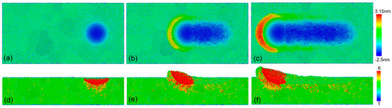
Figure 2.
Deformation behavior of a polycrystalline silicon substrate with average grain size of 4 nm for the scratching distance of 0 nm (a,d); 10 nm (b,e); and 20 nm (c,f) at the scratching depth of 2 nm. In the figures (a–c), atoms are colored according to their heights in the z direction, while in the figures (d–f) atoms are colored according to the coordination number. (a–c) are top views and (d–f) are front views of the polycrystalline silicon.
To study the effect of grain size on the wear process of polycrystalline silicon, we firstly recorded the variations of friction force and normal force for polycrystalline silicon substrate and single-crystal silicon substrate in the wear process, as shown in Figure 3. The forces were calculated by summing the atomic forces of substrate atoms on the tool atoms. The friction force and normal force are defined as the forces parallel to the x direction and the z direction, respectively. Figure 3a,b shows the variation of the typical friction and normal force during the nanoscale wear of silicon substrates. It can be seen that at the initial stage, the friction force increased gradually while the normal force decreased. Then, both the friction force and normal force fluctuated around a constant value. This was mainly due to the change of contact area (number of contact atoms) during the scratching process. It is well known that the friction force and normal force are closely related to the transverse contact area (projected in the scratching direction) and normal contact area (projected in the normal direction), respectively. In the initial stage of scratching, the normal contact area decreased while the transverse contact area increased due to the pile-up in front of the tool. After that, the wear reached a steady stage. The fluctuation of forces during the wear process results mainly from the thermal motion of substrate atoms and plastic deformation. In order to gain deeper insights, we calculated the average friction force and average normal force for polycrystalline and single-crystalline silicon substrates (Figure 3c,d). The friction coefficient [40,41] defined as the ratio of the average friction force to average normal force was also obtained (Figure 3e,f). The average forces were calculated for the scratching distance from 5 to 20 nm where wear was in a steady state. It could be found that for a constant scratching depth, both the average normal force and the friction force were much larger for single-crystalline silicon compared to polycrystalline silicon, which is consistent with the experiments [13,14] and simulation results [22]. It was also found that for the polycrystalline substrates, both the average normal force and the friction force increased with increasing grain size. However, the friction coefficient decreased with increasing grain size, and was the smallest for single-crystalline silicon.
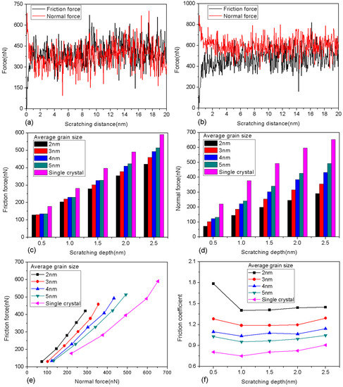
Figure 3.
The friction force and normal force for polycrystalline silicon substrates and single-crystal silicon substrate. (a,b) The force–distance curves for the polysilicon substrate with an average grain size of 4 nm and single-crystal silicon substrate, respectively, at the scratching depth of 2 nm. (c,d) The variation of the average friction force and normal force for polycrystalline silicon substrates with different average grain sizes and single-crystal silicon substrate, respectively. (e) The value of average friction force as a function of normal load. (f) The friction coefficient of polycrystalline silicon substrates and single-crystal silicon substrate as a function of scratching depth.
Note that for metals, the friction coefficient generally increases linearly with scratching depth, as predicted by Bowden and Tabor [42]. However, the friction coefficient for single-crystal silicon showed a rather complicated relationship with scratching depth, as shown in Figure 3f. The friction coefficient first decreased and then increased slightly with scratching depth. This was due to the fact that the friction force grew more slowly than the normal force as the scratching depth increased from 0.5 to 1 nm. Si et al. observed a similar tendency in the scratching of single-crystal silicon using MD simulations [43]. However, the friction force underwent a slightly faster increase than the normal force for scratching depths between 1 and 2.5 nm (Figure 3c,d).
To quantitatively describe how the wear of polycrystalline silicon depends on the grain size, we calculated the number of wear atoms during the wear process. In this work, the substrate atoms that moved on top of the original substrate surface were considered as wear atoms [44]. This is equivalent to the measurements of groove volume or groove depth [45] widely used in wear experiments [24,46]. The quantity of wear atoms was directly proportional to the scratching distance for all the silicon substrates and scratching depths (Figure 4). This is because the wear volume (i.e., total volume of wear atoms) was essentially equal the groove volume on the substrate surface [45]. Furthermore, we present the relation between the quantity of wear atoms and the average normal force for all the substrates in Figure 4f. We observed that the quantity of wear atoms increased nonlinearly with the average normal force, inconsistent with Archard’s law [6,7,8,9,47]. This suggests that Archard’s law is inadequate for describing nanoscale single-asperity wear of silicon substrate. In fact, Archard’s law is a purely empirical equation. Although Archard’s law has been widely used at the macroscale, it has been proven that it fails to model the nanoscale wear mechanisms of silicon (e.g., the atom-by-atom wear process) [7,8,9]. Under the same normal load, the quantity of wear atoms was smaller for polycrystalline substrates with a larger average grain size for the normal loads studied. Moreover, under the same normal load, the quantity of wear atoms of single-crystalline silicon substrate was smaller than that of polycrystalline substrates, which is consistent with the wear experiments by atomic force microscopy [15].
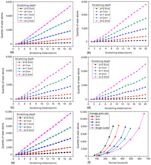
Figure 4.
Data plots for the quantity of wear atoms. (a–d) The wear relations of polycrystalline silicon substrates with average grain sizes of 2 nm, 3 nm, 4 nm, and 5 nm, respectively. (e) The wear relation of single-crystal silicon substrate. (f) The quantity of wear atoms as a function of normal load for different silicon substrates.
To explore the underlying mechanisms behind the effect of grain size on the nanoscale wear of polycrystalline silicon, we analyzed the typical deformation behaviors of polycrystalline silicon (Figure 5). We employed OVITO to identify the diamond structure of silicon [22,24]. It was found that in the wear process, the occurrence of plastic deformation (amorphization) of polycrystalline silicon tended to be along the grain boundaries [21]. In addition, a previous simulation has shown that grain boundaries can reduce the critical stress of plastic deformation of silicon [22]. As a result, plastic deformation takes place more easily for substrates with a smaller average grain size, since the number of grain boundaries is larger for polycrystalline silicon with a smaller grain size. Therefore, both the average friction force and the normal force decreased with the decrease of the average substrate grain size, as shown in Figure 3. This also explains why the quantity of wear atoms increased with the decrease of the average substrate grain size, as shown in Figure 4. Note that the grain size effect of silicon contradicts the Hall–Petch relation. This is because the Hall–Petch effect (grain-boundary strengthening effect) results from the dislocation–dislocation interactions. However, in our simulations of silicon, the main plastic deformation mechanism was not the generation and movement of dislocations.
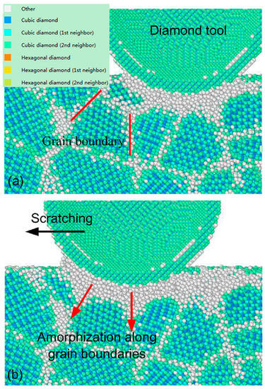
Figure 5.
Deformation behavior of a polycrystalline silicon (a) and the amorphization of silicon along the grain boundary (b). Here the average substrate grain size is 4 nm. The scratching depth is 1 nm. Atoms are colored using theIdentify diamond structure module in OVITO.
4. Conclusions
In this work, MD simulations of the nanoscratching of polycrystalline and single-crystalline silicon substrates using a single-crystal diamond tool were performed to investigate the effect of grain size on the nanoscale wear process of polycrystalline silicon. It was found that for a constant scratching depth, both the average normal force and friction force were much larger for single-crystalline silicon compared to polycrystalline silicon. Furthermore, for the polycrystalline substrates, both the average normal force and friction force increased with increasing grain size. However, the friction coefficient decreased with increasing grain size, and was the smallest for single-crystalline silicon. We also found that the quantity of wear atoms increased nonlinearly with the average normal force, inconsistent with Archard’s law. In the wear process, the pressure-induced phase transformation took place around the tool. The fact that grain boundaries contribute to the occurrence of plastic deformation of polycrystalline silicon can explain the grain size effect in the nanoscale wear of polycrystalline silicon.
Author Contributions
P.Z. designed the simulation cases. P.Z. and H.Y. conducted the simulation. P.Z. wrote the paper. P.Z., R.L. and H.Y. discussed the results and revised the paper.
Acknowledgments
The authors would like to thank Saurav Goel for help with the polycrystalline silicon model. This work is supported by the Fundamental Research Funds for the Central Universities (No. 2018RC001), the Natural Science Foundation of Tianjin (No. 15JCQNJC04800) and National Natural Science Foundation of China (Nos. 51405337, 51875405 and 51475039).
Conflicts of Interest
The authors declare no conflict of interest.
References
- Maboudian, R.; Ashurst, W.R.; Carraro, C. Tribological challenges in micromechanical systems. Tribol. Lett. 2002, 12, 95–100. [Google Scholar] [CrossRef]
- Flater, E.E.; Corwin, A.D.; de Boer, M.P.; Carpick, R.W. In-situ wear studies of surface micromachined interfaces subject to controlled loading. Wear 2006, 260, 580–593. [Google Scholar] [CrossRef]
- de Boer, M.P.; Mayer, T.M. Tribology of MEMS. MRS Bull. 2001, 26, 302–304. [Google Scholar] [CrossRef]
- Archard, J.F. Contact and Rubbing of flat surfaces. J. Appl. Phys. 1953, 24, 981–988. [Google Scholar] [CrossRef]
- Gotsmann, B.; Lantz, M. Atomistic Wear in a Single Asperity Sliding Contact. Phys. Rev. Lett. 2008, 101, 125501. [Google Scholar] [CrossRef] [PubMed]
- Bhaskaran, H.; Gotsmann, B.; Sebastian, A.; Drechsler, U.; Lantz, M.A.; Despont, M.; Jaroenapibal, P.; Carpick, R.W.; Chen, Y.; Sridharan, K. Ultralow Nanoscale Wear through Atom-by-Atom Attrition in Silicon-containing Diamond-like Carbon. Nat. Nanotechnol. 2010, 5, 181–185. [Google Scholar] [CrossRef] [PubMed]
- Jacobs, T.; Carpick, R.W. Nanoscale Wear as a Stress-Assisted Chemical Reaction. Nat. Nanotechnol. 2013, 8, 108–112. [Google Scholar] [CrossRef] [PubMed]
- Chung, K.-H.; Lee, Y.-H.; Kim, D.-E. Characteristics of fracture during the approach process and wear mechanism of a silicon AFM tip. Ultramicroscopy 2005, 102, 161–171. [Google Scholar] [CrossRef] [PubMed]
- Chung, K.H.; Kim, D.E. Fundamental investigation of micro wear rate using an atomic force microscope. Tribol. Lett. 2003, 15, 135–144. [Google Scholar] [CrossRef]
- Liu, J.; Notbohm, J.K.; Carpick, R.W.; Turner, K.T. Method for characterizing nanoscale wear of atomic force microscope tips. ACS Nano 2010, 4, 3763–3772. [Google Scholar] [CrossRef]
- Alsem, D.H.; Stach, E.A.; Dugger, M.T.; Enachescu, M.; Ritchie, R.O. An electron microscopy study of wear in polysilicon microelectromechanicalsystems in ambient air. Thin Solid Films 2007, 515, 3259–3266. [Google Scholar] [CrossRef]
- Alsem, D.H.; vander Hulst, R.; Stach, E.A.; Dugger, M.T.; De Hosson, J.T.M.; Ritchie, R.O. Wear mechanisms and friction parameters for sliding wear of micron-scale polysilicon sidewalls. Sens. Actuators A Phys. 2010, 163, 373–382. [Google Scholar] [CrossRef]
- Bhushan, B. Tribology on the macroscale to nanoscale of microelectromechanical system materials: A review. Proc. Inst. Mech. Eng. Part J J. Eng. Tribol. 2001, 215, 1–18. [Google Scholar] [CrossRef]
- Sundararajan, S.; Bhushan, B. Micro/nanotribological studies of polysilicon and SiC films for MEMS applications. Wear 1998, 217, 251–261. [Google Scholar] [CrossRef]
- Chung, K.H.; Jang, C.E.; Kim, D.E. Wear characteristics of microscopic bushing for MEMS applications investigated by an AFM. J. Micromech. Microeng. 2007, 17, 1877–1887. [Google Scholar] [CrossRef]
- Zhang, L.; Tanaka, H. Atomic scale deformation in silicon monocrystals induced by two-body and three-body contact sliding. Tribol. Int. 1998, 31, 425–433. [Google Scholar] [CrossRef]
- Sun, J.; Fang, L.; Han, J.; Han, Y.; Chen, H.; Sun, K. Abrasive wear of nanoscale single crystal silicon. Wear 2013, 307, 119–126. [Google Scholar] [CrossRef]
- Komanduri, R.; Chandrasekaran, N.; Raff, L.M. Molecular dynamics simulation of the nanometric cutting of silicon. Philos. Mag. B 2001, 81, 1989–2019. [Google Scholar] [CrossRef]
- Tang, Q.; Chen, F. MD simulation of phase transformations due to nanoscale cutting on silicon monocrystals with diamond tip. J. Appl. Phys. 2006, 39, 3674–3679. [Google Scholar] [CrossRef]
- Chrobak, D.; Tymiak, N.; Beaber, A.; Ugurlu, O.; Gerberich, W.W.; Nowak, R. Deconfinement leads to changes in the nanoscale plasticity of silicon. Nat. Nanotechnol. 2011, 6, 480–484. [Google Scholar] [CrossRef]
- Goel, S.; Faisal, N.H.; Luo, X.C.; Yan, J.W.; Agrawal, A. Nanoindentation of polysilicon and single crystal silicon: Molecular dynamics simulation and experimental validation. J. Phys. D Appl. Phys. 2014, 47, 275304. [Google Scholar] [CrossRef]
- Goel, S.; Kovalchenko, A.M.; Stukowski, A.; Cross, G. Influence of microstructure on the cutting behaviour of silicon. Acta Mater. 2016, 105, 464–478. [Google Scholar] [CrossRef]
- Farhat, Z.N.; Ding, Y.; Northwood, D.O.; Alpas, A.T. Effect of grain size on friction and wear of nanocrystalline aluminum. Mater. Sci. Eng. A 1996, 206, 302–313. [Google Scholar] [CrossRef]
- Zhang, Y.S.; Han, Z.; Wang, K.; Lu, K. Friction and wear behaviors of nanocrystalline surface layer of pure copper. Wear 2006, 260, 942–948. [Google Scholar] [CrossRef]
- Ruestes, C.J.; Alhafez, I.A.; Urbassek, H.M. Atomistic Studies of Nanoindentation—A Review of Recent Advances. Crystals 2017, 7, 293. [Google Scholar] [CrossRef]
- Plimpton, S. Fast Parallel Algorithms for Short-Range Molecular Dynamics. J. Comput. Phys. 1995, 117, 1–19. [Google Scholar] [CrossRef]
- Stukowski, A. Visualization and analysis of atomistic simulation data with OVITO-the open visualization tool. Model. Simul. Mater. Sci. Eng. 2010, 18, 015012. [Google Scholar] [CrossRef]
- Schäfer, J.; Stukowski, A.; Albe, K. Plastic deformation of nanocrystalline Pd-Au alloys: On the interplay of grain boundary solute segregation, fault energies and grain size. Acta Mater. 2011, 59, 2957–2968. [Google Scholar] [CrossRef]
- Bussi, G.; Donadio, D.; Parrinello, M. Canonical sampling through velocity-rescaling. J. Chem. Phys. 2007, 126, 014101. [Google Scholar] [CrossRef]
- Tersoff, J. Modeling solid-state chemistry-interatomic potentials for multi-component systems. Phys.Rev. B 1989, 39, 5566–5568. [Google Scholar] [CrossRef]
- Fang, F.Z.; Wu, H.; Liu, Y.C. Modeling and Experimental Investigation on Nanometric Cutting of Single-crystalline Silicon. Int. J. Mach. Tools Manuf. 2005, 45, 1681–1686. [Google Scholar] [CrossRef]
- Rapaport, D.C. The Art of Molecular Dynamics Simulation; Cambridge University Press: Cambridge, UK, 1995. [Google Scholar]
- Zhao, H.; Shi, C.; Zhang, P.; Zhang, L.; Huang, H.; Yan, J. Research on the effects ofmachining-induced subsurface damages on mono-crystalline silicon via molecular dynamics simulation. Appl. Surf. Sci. 2012, 259, 66–71. [Google Scholar] [CrossRef]
- Zhu, P.Z.; Hu, Y.Z.; Ma, T.B.; Wang, H. Study of AFM-based Nanometric Cutting Process using Molecular Dynamics. Appl. Surf. Sci. 2010, 256, 7160–7165. [Google Scholar] [CrossRef]
- Shi, J.; Shi, Y.; Liu, C.R. Evaluation of Three Dimensional Single Point Turning at Atomistic Level by Molecular Dynamics Simulation. Int. J. Adv. Manuf. Technol. 2010, 8, 161–171. [Google Scholar] [CrossRef]
- Tong, Z.; Liang, Y.; Jiang, X.; Luo, X. An Atomistic Investigation on the Mechanism of Machining Nanostructures when using Single Tip and Multi-Tip Diamond Tools. Appl. Surf. Sci. 2014, 290, 458–465. [Google Scholar] [CrossRef]
- Yan, Y.D.; Sun, T.; Dong, S.; Luo, X.C.; Liang, Y.C. Molecular Dynamics Simulation of Processing using AFM Pin Tool. Appl. Surf. Sci. 2006, 252, 7523–7531. [Google Scholar] [CrossRef]
- Fang, T.; Weng, C. Three-Dimensional Molecular Dynamics Analysis of Processing using a Pin Tool on the Atomic Scale. Nanotechnology 2000, 8, 148–153. [Google Scholar] [CrossRef]
- Zhu, P.Z.; Fang, F.Z. Study of the Minimum Depth of Material Removal in nanoscale Mechanical Machining of single crystalline Copper. Comput. Mater. Sci. 2016, 118, 192–202. [Google Scholar] [CrossRef]
- Ewen, J.P.; Gattinoni, C.; Thakkar, F.M.; Morgan, N.; Spikes, H.A.; Dini, D. Nonequilibrium Molecular Dynamics Investigation of the Reduction in Friction and Wear by Carbon Nanoparticles Between Iron Surfaces. Tribol. Lett. 2016, 63, 38. [Google Scholar] [CrossRef]
- Gao, Y.; Brodyanski, A.; Kopnarski, M.; Urbassek, H.M. Nanoscratching of iron: A molecular dynamics study of the influence of surface orientation and scratching direction. Comput. Mater. Sci. 2015, 103, 77–89. [Google Scholar] [CrossRef]
- Bowden, F.P.; Tabor, D. Friction, lubrication and wear: A survey of work during the last decade. Br. J. Appl. Phys. 1966, 17, 1521–1544. [Google Scholar] [CrossRef]
- Si, L.N.; Guo, D.; Luo, J.B.; Lu, X.C. Monoatomic Layer Removal Mechanism in Chemical Mechanical Polishing Process: A Molecular Dynamics Study. J. Appl. Phys. 2010, 107, 064310. [Google Scholar] [CrossRef]
- Zhu, P.Z.; Hu, Y.Z.; Ma, T.B.; Wang, H. Molecular Dynamics Study on Friction due to Ploughing and Adhesion in Nanometric Scratching Process. Tribol. Lett. 2011, 41, 41–46. [Google Scholar] [CrossRef]
- Li, A.; Szlufarska, I. How grain size controls friction and wear in nanocrystalline metals. Phys. Rev. B 2015, 92, 075418. [Google Scholar] [CrossRef]
- Jeng, Y.-R.; Tsai, P.-C.; Chiang, S.-H. Effects of grain size and orientation on mechanical and tribological characterizations of nanocrystalline nickel films. Wear 2013, 303, 262–268. [Google Scholar] [CrossRef]
- Kopta, S.; Salmeron, M. The atomic scale origin of wear on mica and its contribution to friction. J. Chem. Phys. 2000, 113, 8249–8252. [Google Scholar] [CrossRef]
© 2018 by the authors. Licensee MDPI, Basel, Switzerland. This article is an open access article distributed under the terms and conditions of the Creative Commons Attribution (CC BY) license (http://creativecommons.org/licenses/by/4.0/).