Article

Effects of Microsphere Size on the Mechanical Properties of Photonic Crystals

1
Center for Composite Materials and Structure, Science and Technology on Advanced Composites in Special Environment Laboratory, Harbin Institute of Technology, Harbin 150080, China
2
School of Materials Science and Engineering, Harbin Institute of Technology, Harbin 150080, China
3
School of Chemistry and Chemical Engineering, Harbin Institute of Technology, Harbin 150080, China
*
Authors to whom correspondence should be addressed.
Crystals 2018, 8(12), 453; https://doi.org/10.3390/cryst8120453
Submission received: 29 September 2018 / Revised: 2 December 2018 / Accepted: 3 December 2018 / Published: 6 December 2018
(This article belongs to the Section Crystalline Materials)

Abstract

:
Photonic crystal (PC) thin films that are self-assembled from different-sized silica microspheres were prepared for studying mechanical properties via nanoindentation at the submicron scale. We found that the silica photonic crystals (PCs) possessed a face-centered cubic (FCC) microstructure and their elastic modulus and hardness were in the range of ~1.81–4.92 GPa and 0.008–0.033 GPa, respectively. The calculated results proved that there were size-dependent properties in the silica PCs, in that the elastic modulus and hardness increased as the diameter decreased from 538 nm to 326 nm. After studying the total work and plastic work in the progressive deformation of silica PCs during the nanoindentation tests, we developed a two-stage deformation model to explain how the microsphere size affects the mechanical properties of PC thin films. The phenomenon of “smaller is stronger” is mainly due to the energy consumption, which combines the effects of microstructure collapse, microsphere slide, and reduced porosity during the whole loading and unloading process. In addition, the results of numerical simulation matched the experimental data and reflected the energy change rules of PCs during the indentation process. Furthermore, the study affords useful guidance for constructing high-performance films with proper design and potential application in next-generation PC materials.

1. Introduction

In recent decades, photonic crystal (PC) thin films have been investigated extensively because of their potential application in the fields of photonics [1,2,3], thermotics [4,5], electronics [6], and energy conversion [7], as well as sensing technology [8]. The materials for preparing photonic crystals (PCs) can have varied forms, and so is the range of synthetic methods. Up to the present, metals [9], semiconductors [10], polymers [11], and metal oxides [12] with various photonic nanostructures have been reported. PCs can be manufactured typically by top-down or bottom-up techniques. The defect of the top-down method is that it is gradually slower and costlier to produce periodically arranged structures over large areas with increasingly high precision. By comparison, the self-assembly bottom-up technique is widely used in research because of its easy operation and low cost [13]. The self-assembly methods include vertical lifting [14], vertical deposition [15], spin coating [16], and electric and magnetic field induction [17], which are classified systematically based on the driving force. One of the most common and straightforward nanostructures of PCs is an opal structure [18], which has become an essential branch in this field. More complex structures, such as inverse opals [19] and core-shell structure [20], can be constructed to expand the range of applications.
To fabricate functional devices from these materials and take full advantage of their optical, electrical, chemical, and magnetic properties, PCs require suitable mechanical properties. Consequently, an accurate study of the mechanical parameters is essential. However, up till now, mechanical testing of PCs has not been well-established and very little is known about their mechanical properties and governing factors. Furthermore, PCs are brittle, and they cannot yet be produced in a large area with uniform geometry required for uniaxial compression tests [21]. Recently, nanoindentation as an efficient and accurate method, has been widely used for characterizing mechanical properties of materials at the micro/nanoscale [22]. The mechanics of PCs based on nanoindentation have been used; however, the primary application in the existing literature is for assessing the elastic modulus and hardness simply for various synthetic or self-assembly techniques. Nanoindentation has been progressively used for testing some materials that have similar microstructure to PCs, including capped nanocrystals [23], three-dimensional ordered mcriostrucutre (3-DOM) materials [24], ordered silica foam [25], and so on [26,27]. Liu [28,29] studied the size effects via both nanoindentation tests and atomic force microscopy (AFM) indentation tests; he analyzed the stress condition of one single microsphere to explain the size effects but neglected the overall stress condition. To the best of our knowledge, the deformation mechanism of PCs under nanoindentation tests by the energy method has not been studied.
Monodispersed silica microspheres have acquired supremacy over other materials because they are chemically inert and thermally stable. The typical silica PC is a well-knit sphere arranged according to a face-centered cubic (FCC) structure, which is commonly seen in polycrystalline metallic materials [30]. In this study, silica PCs with different microsphere sizes were prepared, the size-dependent phenomenon in representative silica PCs with FCC structure was studied, and the deformation mechanism of silica PCs was explored by a two-stage energy consumption mechanism.

2. Experimental

Monodispersed silica microspheres with diameters of about 326 nm, 348 nm, 437 nm, 470 nm, and 538 nm were synthesized via a modified procedure [31]. First, ammonium solution (25%) was dispersed in an ethanol/water mixture (ratio 7:1) in a reactor under stirring for 30 min at 40 °C, then a mixture of tetraethyl orthosilicate (TEOS,)/ethanol (32 wt%) was added into the reactor. All the reagents were purchased from Sinopharm chemical reagent co. LTD (Beijing, China) without further purification. Different sized silica microspheres were obtained by adjusting the reaction time. Subsequently, the glass slides underwent hydrophilic treatment and were positioned vertically in a vial containing the monodispersed silica suspension, which was carried out in an oven at a constant temperature of 60 °C for 12 h. These silica microspheres were assembly-grown onto the glass substrates to form opal PC thin films by a vertical deposition method [32].
The size and structural features of microspheres were measured by scanning electron microscopy (SEM; FEI Quanta (Hillsborough, OR, USA) 200FEG) at an accelerating voltage of 8 KV. The optical properties of the samples were taken with a fiber spectrometer (Ocean Optics Maya2000 (Dunedin, FL, USA)). Nanoindentation tests were carried out at room temperature with a nanoindenter (Keysight G200 (Santa Clara, CA, USA)) equipped with a Berkovich diamond tip. For each sample, at least five tests were conducted to calculate the average value of the mechanical parameters.

3. Results and Discussion

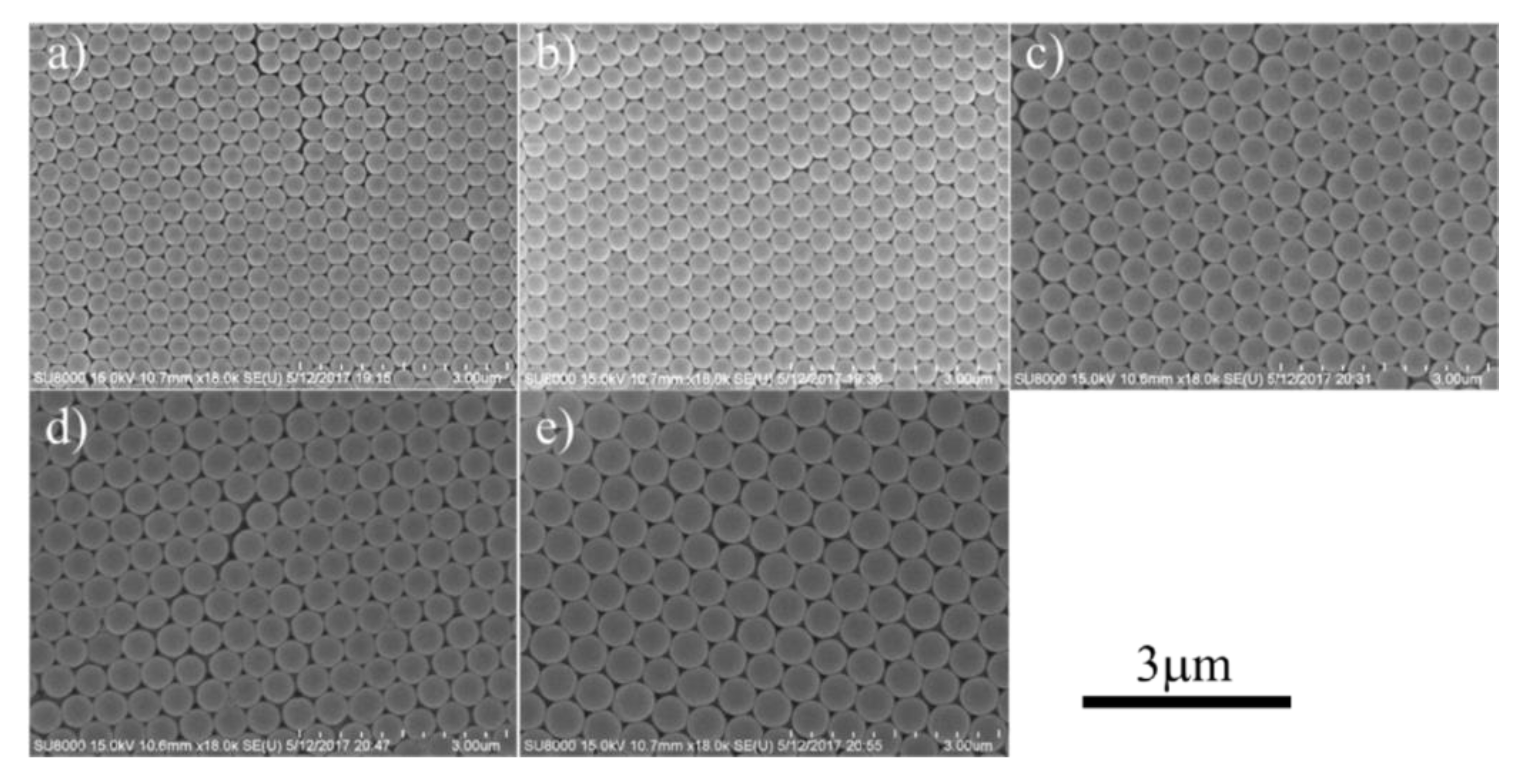
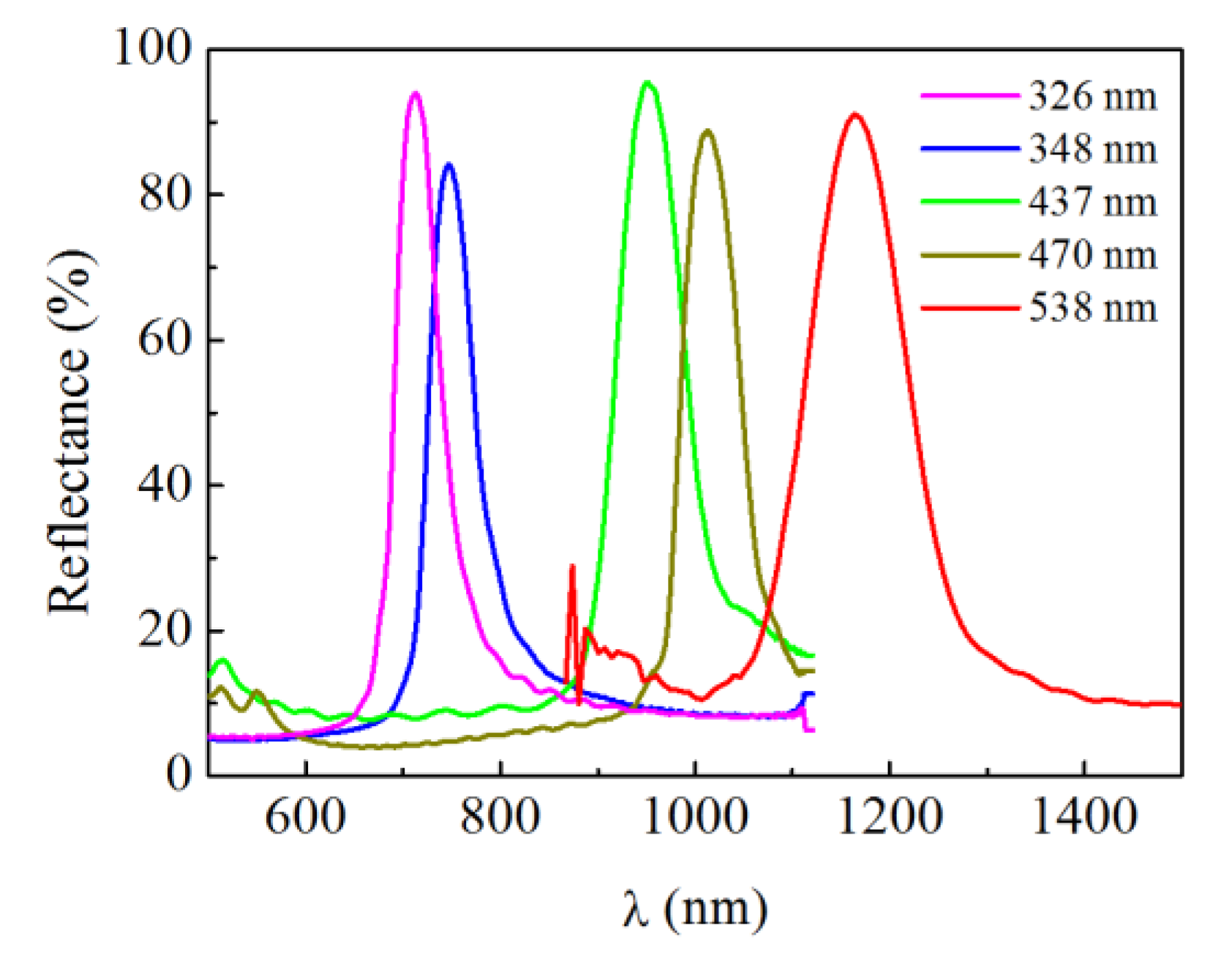
3.1. Structure Features of Silica Photonic Crystals (PCs)

In order to accurately investigate the mechanical properties of silica PC thin films under nanoindentation, high-quality samples were prepared. Note that the PC thin films prepared by flow-induced deposition usually yield a surprisingly strong preference for FCC crystal structure. Characterization of structural features of the PC thin films was conducted to measure the size of microspheres and check a variety of defects of the samples, such as holes, cracks, and pores, which inevitably exist during the preparation process, as shown in Figure 1a–e. Each PC thin film was composed of quite uniformly sized microspheres with size deviation of less than 5%; the diameters of measured microspheres are listed in Table 1. From Figure 1a–e, we can see that the silica microspheres are well-organized in a close-packed arrangement with long-range order.
The optical reflectance spectra of silica PCs are shown in Figure 2. It is obvious that the reflecting peaks of the PCs were located at 712.6 nm, 757.0 nm, 941.2 nm, 1011.1 nm, and 1163.8 nm. According to the results, the reflecting peak showed a redshift from 712.6 nm to 1163.8 nm as the diameter increased from 326.0 nm to 538.0 nm. The reflectance peak values of five PC thin films were all above 85%. This reflectance spectrum suggests the characteristic properties of the photonic band gap, which shows that the fabricated silica PCs are in the ordered arrangement. Theoretically, the position of the photonic band gap in the FCC PCs can be expressed by the Bragg diffraction equation [33]:
k λ = 2 d n e f f 2 sin 2 θ
where λ is the center wavelength of the photonic band gap; k is the order of the Bragg diffraction; d is the (111) plane distance ( d = 2 / 3 D with D being microsphere diameter); θ is the deviated angle from the normal of the (111) planes ( θ = 0° for this study); and n e f f is the average refractive index. In the ideal FCC structure, the n e f f of silica is taken to be 1.33 [34].
The theoretical value of the diameter of the microspheres can be calculated by the Bragg diffraction equation, as shown in Table 1. The experimental values coincide with theoretical values, which indicates that they conform to the FCC structure, also proving the high order of arrangement for PCs. Based on the SEM images, reflection spectra, and theoretical results, it is concluded that the controllable silica PC thin films were well-prepared and appropriate for the mechanical property tests.

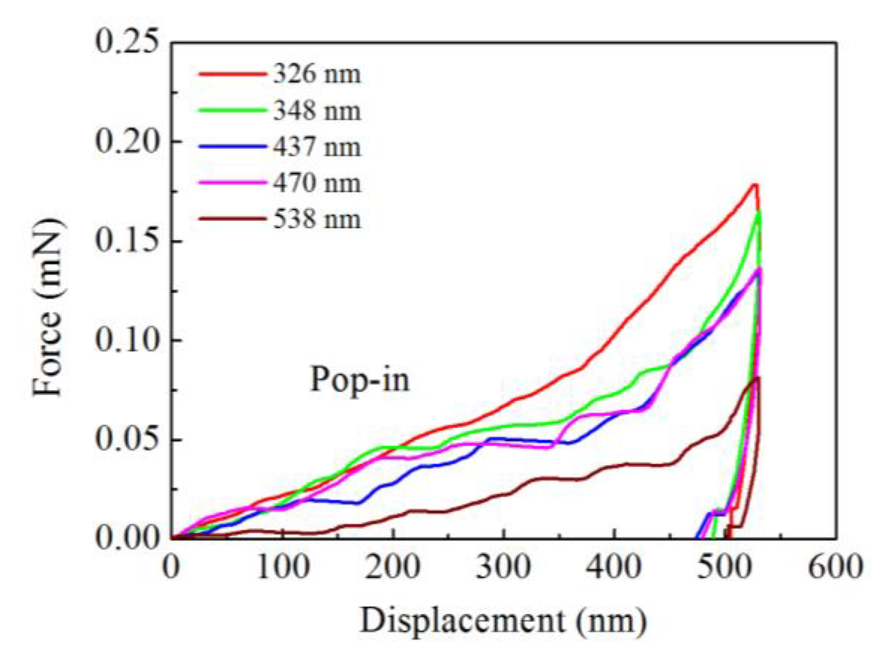
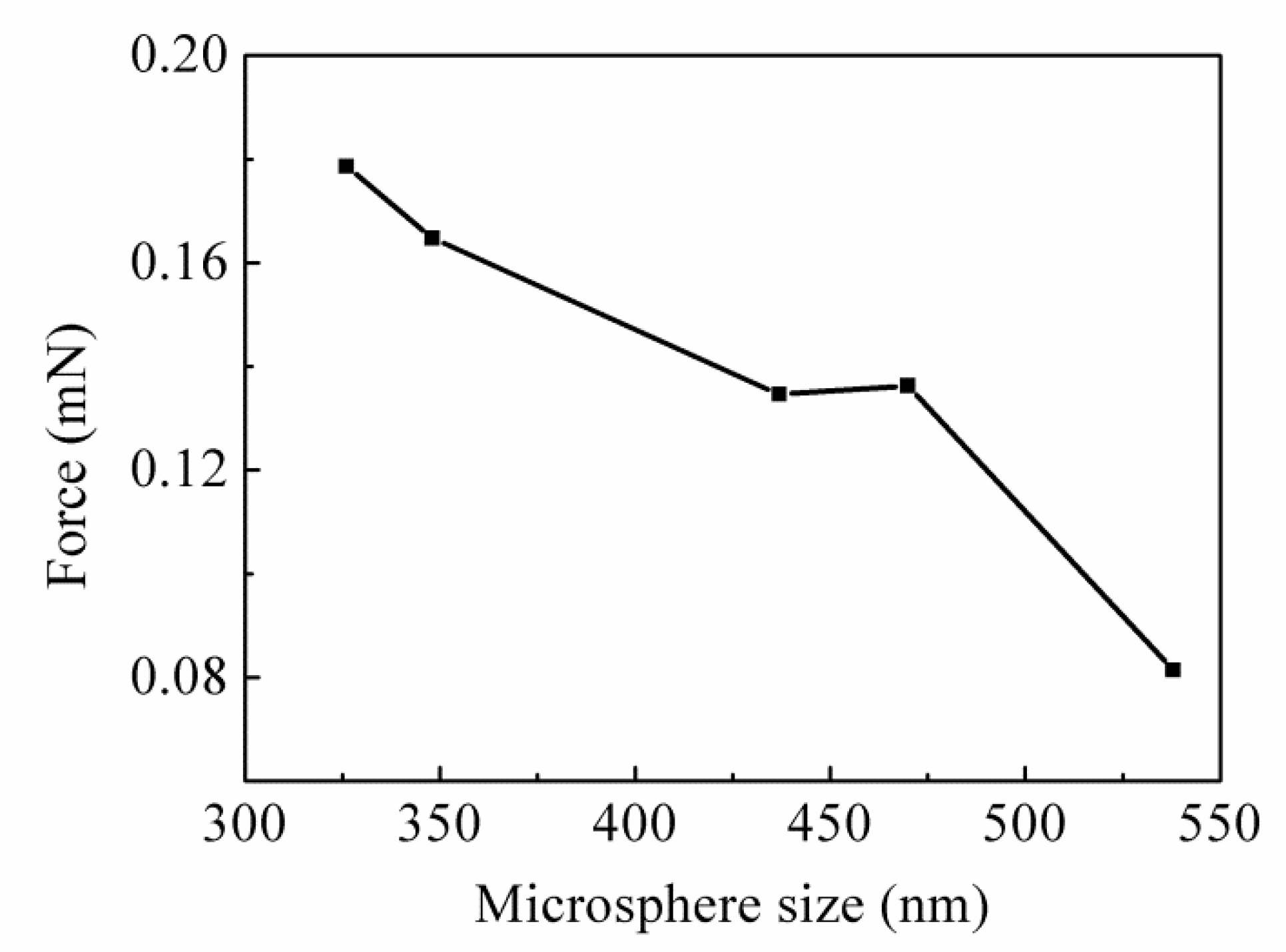
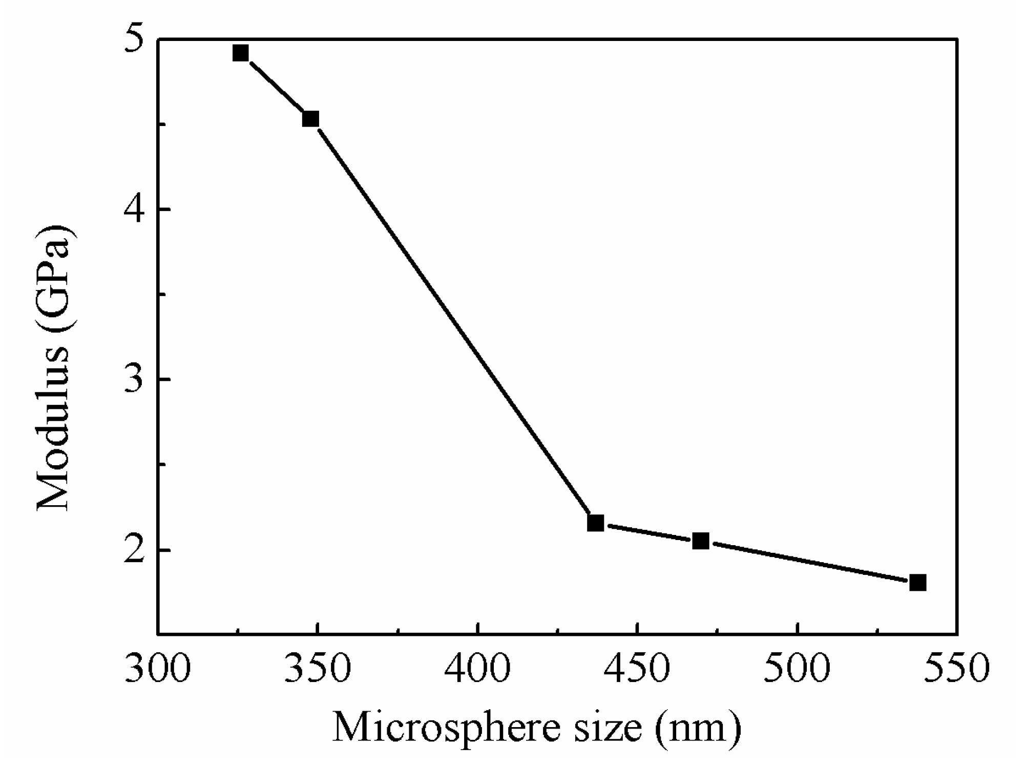
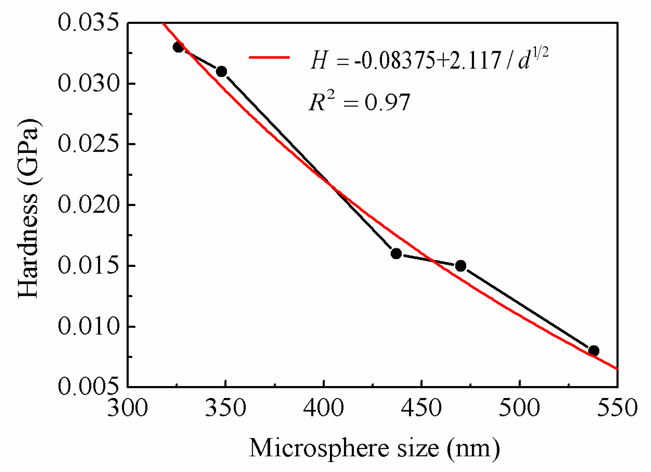
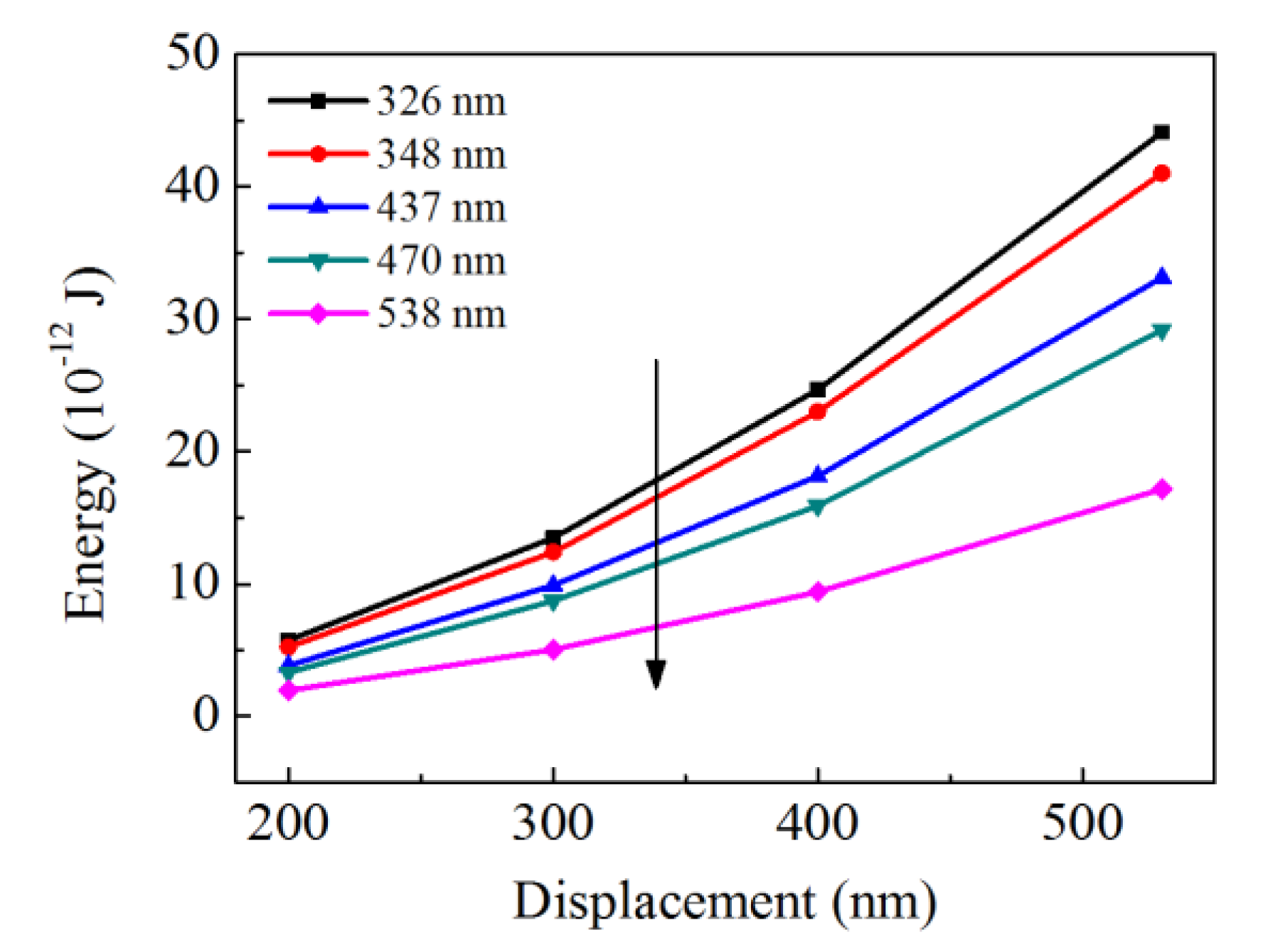
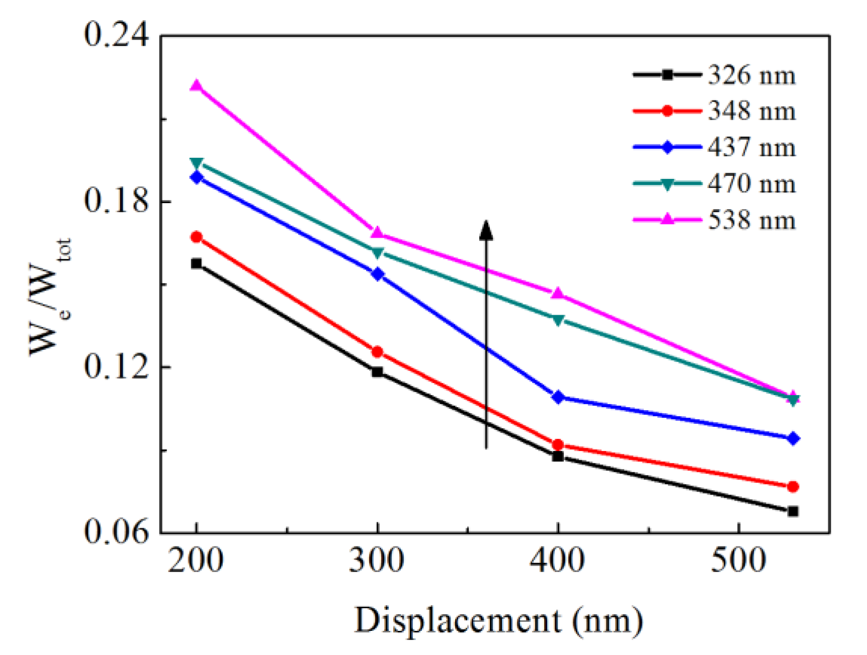
3.2. Size-Dependent Mechanical Properties of Silica PCs

To avoid the substrate effect, the indentation depth should not exceed 10% of the thickness of the samples [33]. In our study, the film thickness was about 10 um and the maximum indentation depth in the tests was set to 550 nm. Thus, the influence of glass substrate on the load-depth curves of the PC thin films was negligible. Figure 3 shows the load-depth curves of five sizes of PC thin films under a maximum indentation depth of 550 nm. Obviously, the loading tracks exhibit a pop-in phenomenon in each curve [35]. Comparing the shape of each curve, there is no pop-in event in the unloading part. It is interesting to find that the curves show a very noticeable size dependence in Figure 4. At the same maximum indentation depth, the load increased significantly as the microsphere size of the PC thin films decreased. Based on the load-depth curves, hardness and Young’s modulus were calculated by applying the Oliver and Pharr method [36]:
H = P max / A
A = 24.56 h c 2
1 E r = 1 υ 2 E + 1 υ i 2 E i
where H is the hardness; P max is the peak load; h c is the contact depth; A is the contact area; E r is the reduced modulus, E r = S π / ( 2 β A ) ; β is a constant related to indenter shape, β = 1.034 when using a Berkovich diamond tip; S is the curvature of the unloading curve; E and υ are the elastic modulus and Poisson ratio of the samples, υ = 0.3 ; and E i and υ i are the elastic modulus and Poisson ratio of the diamond indenter, υ i = 0.07 , E i = 1141   GPa .
Figure 5 shows the measured Young’s modulus for different PC thin films. The Young’s modulus decreased when the size of the constitutive microspheres increased. The calculated results prove unambiguously that the elastic modulus of PCs is strong and dependent on size, increasing from 1.81 GPa to 4.92 GPa as the diameter decreased from 538 nm to 326 nm. Likewise, hardness demonstrated a similar size-dependent tendency, increasing from 0.008 GPa to 0.033 GPa as the diameter decreased, as shown in Figure 6. The relation between the yield stress and the grain size in the PCs is known as the Hall–Petch relation [37,38]. The empirical Hall–Petch formula states that yield strength increases monotonically with decreased average grain size according to
σ y = σ o + k / d 1 / 2
where σ o is the friction stress and k is a material constant.
In light of the scaling approach to conical indentations in elastic–plastic solids by Cheng-Cheng [38], the relationship between hardness and yield stress is given by
H = a σ y
where a is a constant from 1 to 3, conditional on the ratio of σ y / E .
Based on this linear correlation, using Equations (5) and (6), we obtain
H = a σ o + a k / d 1 / 2 = B + C / d 1 / 2
where B and C are constants dependent on materials.
We fit the constant values B and C by the relationship between hardness and microsphere size. From Figure 6, we can see that the relationship between microsphere size and hardness is similar to the Hall-Petch formula. Our investigation revealed that the trend “smaller is stronger” occurred in silica PCs, similar to the result of Liu [28], which had been extensively reported for crystalline metallic materials [39,40].

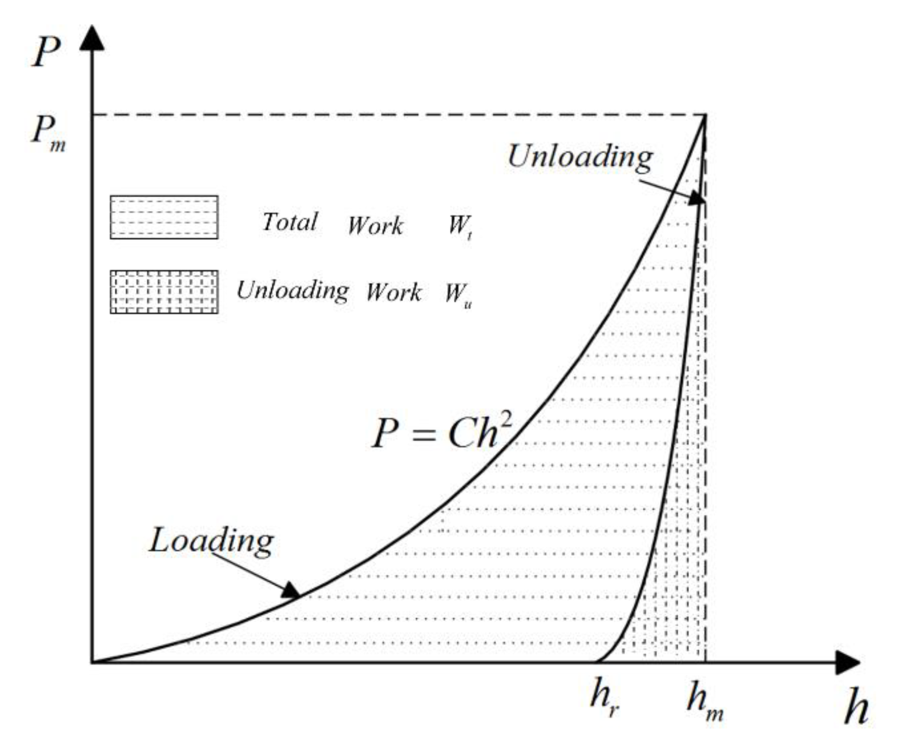
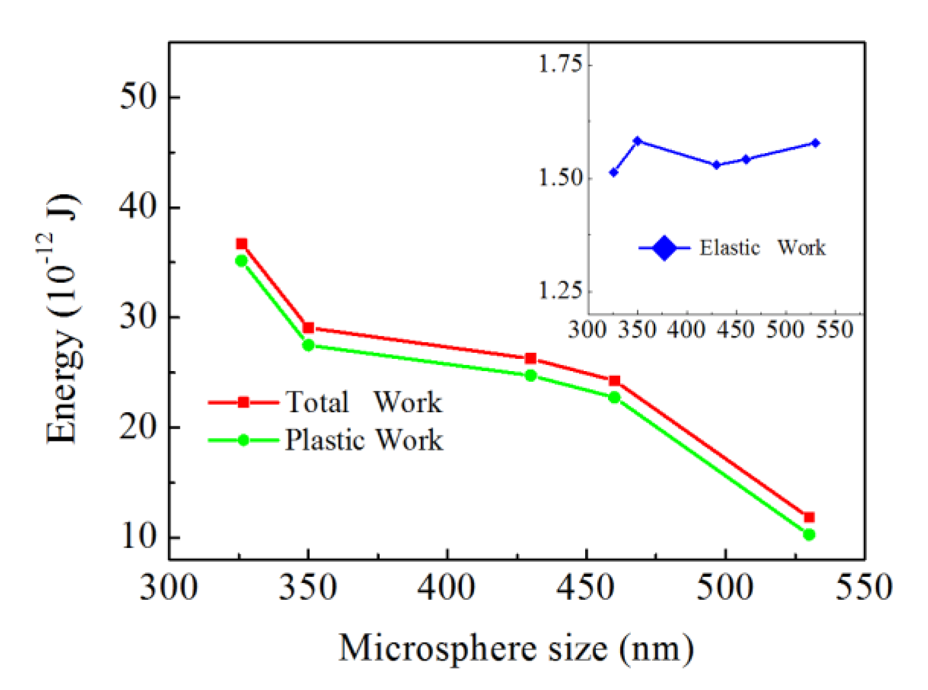
3.3. Deformation Mechanisms

As presented in the previous sections, mechanical properties, including load–depth curves, Young’s modulus, and hardness, were equally size-independent. The mechanical properties of this “granular” material depend on the contacts and adhesion between the particles at nanoscale. However, the silica PCs at submicron level contain specific microstructures, and their mechanical properties are affected by both microsphere size and microstructures. Furthermore, the synthesis of these silica PCs has the same porosities intended to be kept as constant (0.26) because of the FCC structure [41], which indicates that the mechanical properties of silica PCs are mainly affected by the variations of particle size and the intrinsic mechanical parameters of microspheres. However, the deformation under the tip is a complex nonlinear process, including elastic and multiple plastic deformations. In order to explore its mechanism, we studied the total work and plastic work in the progressive failure of silica PCs. The area under the loading curve gives the total work W t , as shown in Figure 7; the reversible elastic work W e can be deduced from the area under the unloading curve [42]. The energy absorbed by plastic deformation is the difference between these: W p = W t W e
W t = 0 h m P l o a d i n g d h
W ε = h r h m P u n l o a d i n g d h
where h m is the maximum depth, h r is the final depth at which the force on the indenter first becomes zero during unloading, P l o a d i n g is the loading function, and P u n l o a d i n g is the unloading function.
In Figure 8, it is found that the elastic work of the material accounts for a lower proportion than that of plastic work during the entire indentation process. It is worth noting that the elastic work of the microspheres is almost the same. However, the total work and plastic work decrease gradually with increased particle size, indicating that the deformation resistance under the indenter is weakened. Furthermore, we propose a two-stage deformation model under the tip in the progress of nanoindentation. The first stage is achieving the yield strength of the silica microspheres, and the second stage is disruption of the PC microstructure. Silica microspheres are brittle, and the material will soon reach yield state with the increase in external stress, then the microspheres begin to break, and slight cracks occur, accompanied by the dissipation of energy. In this way, the deformation in the first stage is completed rapidly, and the elastic work occupies the leading part in this stage. Subsequently, the microstructure collapses and the microspheres break up into numerous small pieces with the deepening of the indenter, resulting in increased film density and reduced porosity. Furthermore, relative sliding and rotation occur among the small pieces, and friction continuously consumes energy; the film shrinks in volume as a whole, and its resistance to deformation increases continuously. In the second stage, the plastic work occupies the central part, and the influence of elastic work can be ignored. When the microsphere diameter is larger, the microsphere also suffers elastic–plastic deformation and goes through crack development. Energy consumption is consistent in the first stage; this conjecture can be proved by the value of elastic work in Figure 8. However, in the second stage of destruction, the film density also increases after crushing, with relatively small amplification. Thus, energy consumption in the second stage is lower and material resistance to deformation decreases, resulting in a reduction of its hardness and modulus. This energy consumption principle is similar to the Hall–Petch strengthening theory, which is usually used for polycrystalline metallic materials; smaller microspheres have more particle boundaries and more density after crushing. Destruction in the second stage goes on along with the first stage by deepening of the indenter because of extrusion between the microspheres, leading to the pop-in phenomenon, that is, several jumps during each loading curve, as shown in Figure 3.
The energy value of Figure 8 is calculated based on the experimental results at the maximum indentation depth, so it cannot reflect the energy change rules of PCs during the entire indentation process. Therefore, in the plastic work and total work, the finite element method (FEM) simulation of PCs is presented to investigate the relations between and among the elastic work (Supplementary Materials). We selected four indentation depths to simulate the indentation process and then calculated the work of each part according to the simulation curves. As shown in Figure 9, total work gradually increased with increased indentation depth in all cases; however, with rising microsphere size, whole work decreased in the same indentation depth. This illustrates that under the same depth of penetration, the energy of resistance to deformation decreased with the increased particle size, resulting in less hardness and smaller elastic modulus. It obviously shows that at a depth of 200 nm the total energy of these five microspheres was below 10 × 10–12 J, between 1.938 × 10⁻¹² J and 5.762 × 10⁻¹² J. However, the work value of the different microsphere sizes began to change significantly with the increase in depth, and this was because the second-stage deformation became the primary factor. From Figure 10, it can be concluded that the proportion of elastic work gradually decreased with the increase of indentation depth, and the ratio was down to less than 10% at the maximum indentation displacement. This indicates that the plastic proportion is more significant due to the second-stage deformation. With the decrease of microsphere size, the proportion of elastic work decreased, so the plasticity ratio increased. Although the areas under the indenter at the same penetration depth were equal, the void ratio changed after the microsphere was broken. The smaller the particle size, the higher the density, with a lower proportion of elastic work. These trends coincide with the two-stage deformation model and the experimental results. Therefore, the simulation results prove the effectiveness of the two-stage deformation model.

4. Conclusions

In conclusion, silica PC thin films with periodic FCC structure were prepared from microspheres with five different sizes. The relationship between the size of the microspheres and the mechanical properties of the PCs was explored by nanoindentation. The results show that silica PCs with smaller microspheres possess enhanced hardness and modulus, suggesting a noticeable size-dependent mechanical performance. The two-stage deformation assumption of silica PCs under the indenter is presented to explain the size-dependent property due to the trend of energy change. The phenomenon may mainly result from energy consumption, which includes microstructure collapse, microsphere slide, and reduced film porosity during the whole loading and unloading process. FEM results prove this deformation tendency. This study also indicates that the mechanical properties of PCs with the proper design of microsphere size could be further tuned to suit the application of advanced devices.

Supplementary Materials

The following are available online at https://www.mdpi.com/2073-4352/8/12/453/s1, Figure S1: The geometric model of colloidal crystals. Figure S2: The simulation curves under different indention depth (a) 326 nm, (b) 347 nm, (c) 438 nm, (d) 470 nm, (e) 538 nm.

Author Contributions

Conceptualization, Y.W. and S.D.; Methodology, Y.W.; Software, Y.W.; Validation, Y.L., J.Z. and K.Z.; Formal Analysis, L.S.; Investigation, P.Z.; Resources, Y.L.; Data Curation, J.Z.; Writing-Original Draft Preparation, Y.W.; Writing-Review & Editing, K.Z.; Visualization, K.Z.; Supervision, X.Y.; Project Administration, Y.L.; Funding Acquisition, Y.L.

Funding

This research was funded by the National Natural Science Foundation of China (No. 51572058, 51502057, 51761135123), the National Key Research & Development Program (2016YFB0303903, 2016YFE0201600), the International Science & Technology Cooperation Program of China (2013DFR10630, 2015DFE52770), and the Foundation of Equipment Development Department (6220914010901).

Conflicts of Interest

The authors declare no conflicts of interest

References

  1. Yablonovitch, E.; Gmitter, T.J. Photonic band structure: The face-centered-cubic case. Phys. Rev. Lett. 1989, 63, 1950–1953. [Google Scholar] [CrossRef] [PubMed]
  2. Saviot, L.; Le Gallet, S.; Demoisson, F.; David, L.; Sudre, G.; Girard, A.; Margueritat, J.; Mermet, A. Inelastic light scattering contribution to the study of the onset of sintering of a nanopowder. J. Phys. Chem. C 2017, 121, 2487–2494. [Google Scholar] [CrossRef]
  3. Alonso-Redondo, E.; Huesmann, H.; El Boudouti, E.H.; Tremel, W.; Djafari-Rouhani, B.; Butt, H.J.; Fytas, G. Phoxonic hybrid superlattice. ACS Appl. Mater. Interfaces 2015, 7, 12488–12495. [Google Scholar] [CrossRef] [PubMed]
  4. Poyser, C.L.; Czerniuk, T.; Akimov, A.; Diroll, B.T.; Gaulding, E.A.; Salasyuk, A.S.; Kent, A.J.; Yakovlev, D.R.; Bayer, M.; Murray, C.B. Coherent acoustic phonons in colloidal semiconductor nanocrystal superlattices. ACS Nano 2016, 10, 1163–1169. [Google Scholar] [CrossRef]
  5. Ayouch, A.; Dieudonné, X.; Vaudel, G.; Piombini, H.; Vallé, K.; Gusev, V.; Belleville, P.; Ruello, P. Elasticity of an assembly of disordered nanoparticles interacting via either van der waals-bonded or covalent-bonded coating layers. ACS Nano 2012, 6, 10614–10621. [Google Scholar] [CrossRef] [PubMed]
  6. Gao, Y.; Shiue, R.J.; Gan, X.; Li, L.; Peng, C.; Meric, I.; Wang, L.; Szep, A.; Walker, D., Jr.; Hone, J.; et al. High-speed electro-optic modulator integrated with graphene-boron nitride heterostructure and photonic crystal nanocavity. Nano Lett. 2015, 15, 2001–2005. [Google Scholar] [CrossRef] [PubMed]
  7. Nam, Y.; Yeng, Y.X.; Lenert, A.; Bermel, P.; Celanovic, I.; Soljačić, M.; Wang, E.N. Solar thermophotovoltaic energy conversion systems with two-dimensional tantalum photonic crystal absorbers and emitters. Sol. Energy Mater. Sol. Cells 2014, 122, 287–296. [Google Scholar] [CrossRef]
  8. Fenzl, C.; Hirsch, T.; Wolfbeis, O.S. Photonic crystals for chemical sensing and biosensing. Angew. Chem. Int. Ed. Engl. 2014, 53, 3318–3335. [Google Scholar] [CrossRef]
  9. López, C. Materials Aspects of Photonic Crystals. Adv. Mater. 2003, 15, 1679–1704. [Google Scholar] [CrossRef]
  10. Birowosuto, M.D.; Yokoo, A.; Zhang, G.; Tateno, K.; Kuramochi, E.; Taniyama, H.; Takiguchi, M.; Notomi, M. Movable high-Q nanoresonators realized by semiconductor nanowires on a Si photonic crystal platform. Nat. Mater. 2014, 13, 279–285. [Google Scholar] [CrossRef] [Green Version]
  11. Fang, Y.; Ni, Y.; Leo, S.Y.; Taylor, C.; Basile, V.; Jiang, P. Reconfigurable photonic crystals enabled by pressure-responsive shape-memory polymers. Nat. Commun. 2015, 6, 7416. [Google Scholar] [CrossRef] [PubMed] [Green Version]
  12. Falcaro, P.; Ricco, R.; Yazdi, A.; Imaz, I.; Furukawa, S.; Maspoch, D.; Ameloot, R.; Evans, J.D.; Doonan, C.J. Application of metal and metal oxide nanoparticles@MOFs. Coord. Chem. Rev. 2016, 307, 237–254. [Google Scholar] [CrossRef] [Green Version]
  13. Von Freymann, G.; Kitaev, V.; Lotsch, B.V.; Ozin, G.A. Bottom-up assembly of photonic crystals. Chem. Soc. Rev. 2013, 42, 2528–2554. [Google Scholar] [CrossRef] [PubMed] [Green Version]
  14. Cheng, W.; Wang, J.; Jonas, U.; Fytas, G.; Stefanou, N. Observation and tuning of hypersonic bandgaps in colloidal crystals. Nat. Mater. 2006, 5, 830. [Google Scholar] [CrossRef] [PubMed]
  15. Liu, G.; Shao, J.; Zhang, Y.; Wu, Y.; Wang, C.; Fan, Q.; Zhou, L. Self-assembly behavior of polystyrene/methacrylic acid (P(St-MAA)) colloidal microspheres on polyester fabrics by gravitational sedimentation. J. Text. Inst. 2015, 106, 1293–1305. [Google Scholar] [CrossRef]
  16. Yang, S.; Moon, J.H. Chemical Aspects of Three-Dimensional Photonic Crystals. Chem. Rev. 2010, 10, 547–574. [Google Scholar]
  17. Ge, J.; Yin, Y. Responsive photonic crystals. Angew. Chem. Int. Ed. Engl. 2011, 50, 1492–1522. [Google Scholar] [CrossRef] [PubMed]
  18. Sui, N.; Wang, Y.-H.; Song, Y.-F.; Wang, F.-Y.; Ma, Y.-G.; Zhang, H.-Z. Manipulating fluorescence characteristics of conjugated fluorescent molecules incorporated into three-dimensional poly(methyl methacrylate) opal photonic crystals. Appl. Phys. Express 2014, 7, 025202. [Google Scholar] [CrossRef]
  19. Chaouachi, A.; Chtourou, R.; M’nif, A.; Hamzaoui, A.H. Optimal enhancement in conversion efficiency of crystalline Si solar cells using inverse opal photonic crystals as back reflectors. J. Opt. 2015, 17, 045106. [Google Scholar] [CrossRef]
  20. Li, F.; Josephson, D.P.; Stein, A. Colloidal assembly: The road from particles to colloidal molecules and crystals. Angew. Chem. Int. Ed. Engl. 2011, 50, 360–388. [Google Scholar] [CrossRef] [PubMed]
  21. Orlin, E.W.K.; Velev, D. Structured Porous Materials via Colloidal Crystal Templating: From Inorganic Oxides to Metals. Adv. Mater. 2000, 12, 531–534. [Google Scholar]
  22. Oliver, W.C.; Pharr, G.M. Measurement of hardness and elastic modulus by instrumented indentation: Advances in understanding and refinements to methodology. J. Mater. Res. 2011, 19, 3–20. [Google Scholar] [CrossRef]
  23. Podsiadlo, P.; Krylova, G.; Lee, B.; Critchley, K.; Gosztola, D.J.; Talapin, D.V.; Ashby, P.D.; Shevchenko, E.V. The Role of Order, Nanocrystal Size, and Capping Ligands in the Collective Mechanical Response of Three-Dimensional Nanocrystal Solids. J. Am. Chem. Soc. 2010, 132, 8953–8960. [Google Scholar] [CrossRef] [PubMed]
  24. Li, Y.; Ma, B.; Zhao, J.; Xin, W.; Wang, X. Excellent mechanical properties of three-dimensionally ordered macroporous nickel photonic crystals. J. Alloys and Compd. 2011, 509, 290–293. [Google Scholar] [CrossRef]
  25. Toivola, Y.; Stein, A.; Cook, R.F. Depth-sensing indentation response of ordered silica foam. J. Mater. Res. 2011, 19, 260–271. [Google Scholar] [CrossRef]
  26. Zhou, H.; Pei, Y.; Fang, D. Magnetic field tunable small-scale mechanical properties of nickel single crystals measured by nanoindentation technique. Sci. Rep. 2014, 4, 4583. [Google Scholar] [CrossRef] [PubMed]
  27. Lee, J.H.; Wang, L.; Kooi, S.; Boyce, M.C.; Thomas, E.L. Enhanced energy dissipation in periodic epoxy nanoframes. Nano Lett. 2010, 10, 2592–2597. [Google Scholar] [CrossRef] [PubMed]
  28. Liu, M.; Xu, W.; Bai, J.; Chua, C.K.; Wei, J.; Li, Z.; Gao, Y.; Kim, D.H.; Zhou, K. Investigation of the size effect for photonic crystals. Nanotechnology 2016, 27, 405703. [Google Scholar] [CrossRef]
  29. Liu, M.; Lin, J.-y.; Lu, C.; Tieu, K.; Zhou, K.; Koseki, T. Progress in Indentation Study of Materials via Both Experimental and Numerical Methods. Crystals 2017, 7, 258. [Google Scholar] [CrossRef]
  30. Marnier, G.; Keller, C.; Taleb, L. Tensile prestrain memory effect on subsequent cyclic behavior of FCC metallic materials presenting different dislocations slip modes. Int. J. Plast. 2016, 78, 64–83. [Google Scholar] [CrossRef]
  31. Pan, L.; Wang, Y.; Xu, H.-B.; Ding, Y.-b.; Li, Y.; Zhao, J.-P. Synthesis of Silica Particles with Precisely Tailored Diameter. Chin. J. Chem. Phys. 2014, 27, 563–567. [Google Scholar] [CrossRef]
  32. Wong, S.; Kitaev, V.; Ozin, G.A. Ozin, Colloidal Crystal Films: Advances in Universality and Perfection. J. Am. Chem. Soc. 2003, 125, 15589–15598. [Google Scholar] [CrossRef] [PubMed]
  33. Li, Y.; Valavala, P.; Watcharotone, S.; Brinson, L.C. Models for nanoindentation of compliant films on stiff substrates. J. Mater. Res. 2015, 30, 1747–1760. [Google Scholar] [CrossRef]
  34. Astratov, V.N.; Vlasov, Y.A.; Karimov, O.Z.; Kaplyanskii, A.A.; Musikhin, Y.G.; Berth, N.A.; Bogomolov, V.N.; Prokofiev, A.V. Photonic band gaps in 3D ordered fee silica matrices. Phys. Lett. A 1996, 222, 349–353. [Google Scholar] [CrossRef]
  35. Abram, R.; Chrobak, D.; Nowak, R. Origin of a Nanoindentation Pop-in Event in Silicon Crystal. Phys. Rev. Lett. 2017, 118, 095502. [Google Scholar] [CrossRef]
  36. Oliver, W.C.; Pharr, G.M. An improved technique for determining hardness and elastic modulus using load and displacement sensing indentation experiments. J. Mater. Res. 2011, 7, 1564–1583. [Google Scholar] [CrossRef]
  37. Mohammadabadi, A.S.; Dehghani, K. A New Model for Inverse Hall-Petch Relation of Nanocrystalline Materials. J. Mater. Eng. Perform. 2008, 17, 662–666. [Google Scholar] [CrossRef]
  38. Padmanabhan, K.A.; Sripathi, S.; Hahn, H.; Gleiter, H. Inverse Hall–Petch effect in quasi- and nanocrystalline materials. Mater. Lett. 2014, 133, 151–154. [Google Scholar] [CrossRef]
  39. Maaß, R.; van Petegem, S.; Ma, D.; Zimmermann, J.; Grolimund, D.; Roters, F.; van Swygenhoven, H.; Raabe, D. Smaller is stronger: The effect of strain hardening. Acta Mater. 2009, 57, 5996–6005. [Google Scholar] [CrossRef]
  40. Raghavan, R.; Kirchlechner, C.; Jaya, B.N.; Feuerbacher, M.; Dehm, G. Mechanical size effects in a single crystalline equiatomic FeCrCoMnNi high entropy alloy. Scr. Mater. 2017, 129, 52–55. [Google Scholar] [CrossRef]
  41. Gao, W.; Rigout, M.; Owens, H. Self-assembly of silica colloidal crystal thin films with tuneable structural colours over a wide visible spectrum. Appl. Surf. Sci. 2016, 380, 12–15. [Google Scholar] [CrossRef] [Green Version]
  42. Jha, K.K.; Suksawang, N.; Lahiri, D.; Agarwal, A. A novel energy-based method to evaluate indentation modulus and hardness of cementitious materials from nanoindentation load–displacement data. Mater. Struct. 2014, 48, 2915–2927. [Google Scholar] [CrossRef]
Figure 1. Scanning electron microscopy images (SEM) of silica photonic crystal (PC) thin films assembled from microspheres with sizes of (a) 326 nm, (b) 348 nm, (c) 437 nm, (d) 470 nm, and (e) 538 nm.
Crystals 08 00453 g001
Figure 2. Reflectance spectra of five sizes of photonic crystals assembled from silica microspheres.
Crystals 08 00453 g002
Figure 3. Indentation load-displacement curves of silica photonic crystals (PCs) with a Berkovich tip.
Crystals 08 00453 g003
Figure 4. Maximum load changes with microsphere size.
Crystals 08 00453 g004
Figure 5. Young’s modulus changes with the size of microspheres.
Crystals 08 00453 g005
Figure 6. Hardness changes with the size of microspheres.
Crystals 08 00453 g006
Figure 7. Sketch of indentation work.
Crystals 08 00453 g007
Figure 8. Changes in work value for different diameters of microspheres.
Crystals 08 00453 g008
Figure 9. Total work varies with change of indentation depth for five microsphere sizes.
Crystals 08 00453 g009
Figure 10. Ratio of elastic work to total work at different indentation depths.
Crystals 08 00453 g010
Table 1. Comparison of microsphere diameters obtained by theoretical calculation and experimental measurement.
SampleTheoretical Value (nm)Experimental Value (nm)Error Rate (%)
13283260.6
23493480.2
34334370.8
44664690.8
55365380.4

