1. Introduction
The photomask is a cost component in the patterning of optoelectronic devices [
1,
2,
3]. With the booming market of liquid crystal display (LCD) TVs moving toward large panels, the geometric complexity of the photomask increases continuously. If a protrusive defect adhered onto the substrate went through the photolithography process, the photomask will be damaged [
4,
5] without warning and would result in dramatic losses.
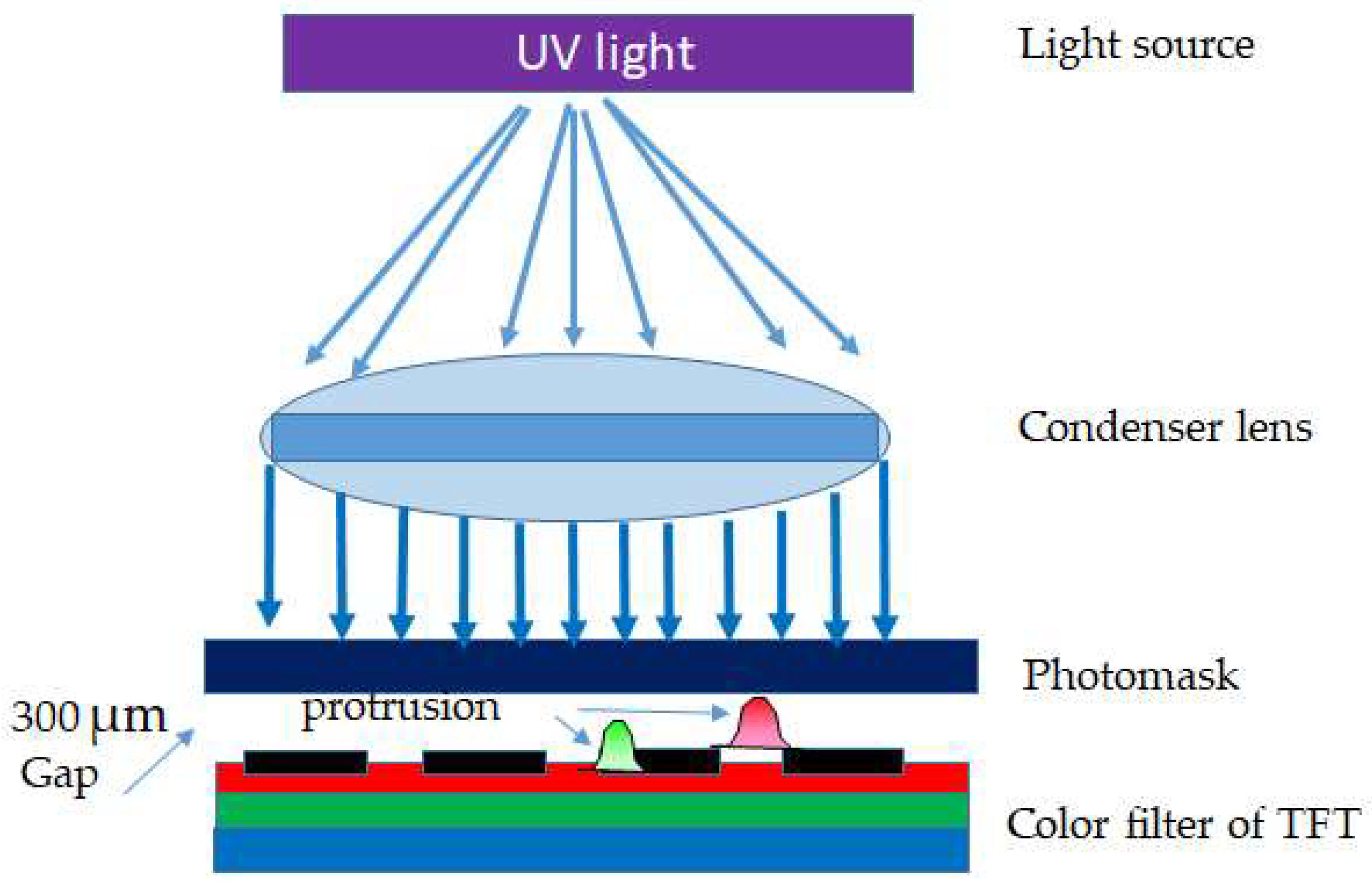
Figure 1 illustrates the mask scratches in the depth of field (DOF) at 300 μm between the substrate and photomask due to the presence of protrusions. Practically, DOF depends on the requirement of the proximity-type aligner; normally the gap is from 100 μm to 350 μm in various products.
Among the protrusive defects, statistics indicate that fragmented glass comprises 70%, metal particles 20%, and others 10% in the production line. That is to say, the fragmented glass is the key factor in damaging the photomask. Efforts were made to delineate the related defect issues in the literature. For example, Cabral et al. [
6] utilized a computer vision system (CVT) for edge detection to detect glass particles in glass products used in food packaging. It is a low-cost system which consists of a conveyor belt and a PC-controlled camera. By converting the grayscale image into a binary format, the detection rate for the glass particles is 90%.
Furthermore, Wang and Tay [
7] utilized an optical interferometric system using a Mireau objective to measure the surface profile of the micro-components. The accuracy of their measurements on standard blocks is comparable to an existing commercial white-light interferometer and a stylus profilometer. Ishii [
8] measured the protrusion’s 3D shape using a shape-from-focus scheme, in which the focused-section method could shrink the shape contour. A ridge of 200 μm in height could be measured with a precision of 20 μm using an area charge-coupled device (CCD). Ahmad and Choi [
9] proposed a 3D window for finding the best focusing points and applied it to a camera-mounted microscope for auto-grinding equipment of LCD color filters. Zhang et al. [
10] implemented and compared six known shapes from shading algorithms. The performance of the algorithms was evaluated by synthetic images using the mean and standard deviation of the depth error, the mean of the surface gradient error, and the central processor unit timing.
In this study, we present a fast method to detect the protrusive defect to prevent photomask damage using a non-contact detection engaged in a CCD-based area. A cost-effective mechanism is installed on top of the platform using the side-view illumination method with an optical reflection in the dark field [
11,
12]. Moreover, not only can accurate results be obtained for in-line production in a timely fashion, but, additionally, the hardware equipment can be varied to accommodate different protrusive heights for any color filter film in TFT-LCDs.
2. Principle
This study utilizes the geometric reflectance optics to approach the albedo. The irradiance,
I, is defined as the incident flux density (W/m
−2) as follows [
13]:
The symbol
dϕi is the flux incident on the area (
dA). The principle is based on the reflective shade to map an image with gray variation using CCD [
8,
10]. After acquiring the image, the embedded algorithm computes the gray intensity for each pixel. Each gray level takes the baseline as the threshold. If the gray level is larger than the threshold, the level will be counted into the effective pixel. The average gray level of the effective pixels converts a relative length in the range of 0–300 μm of the protrusion with respect to the 0–255 gray level. The average gray level is computed by Equation (2), in which
Npixel denotes the effective pixels for which the gray level is greater than the threshold and
Gi labels the gray summation for the effective pixel
Npixel.
The
Averagegray represents the relative length of the effective pixel while we perform the area conversion from square to circular.
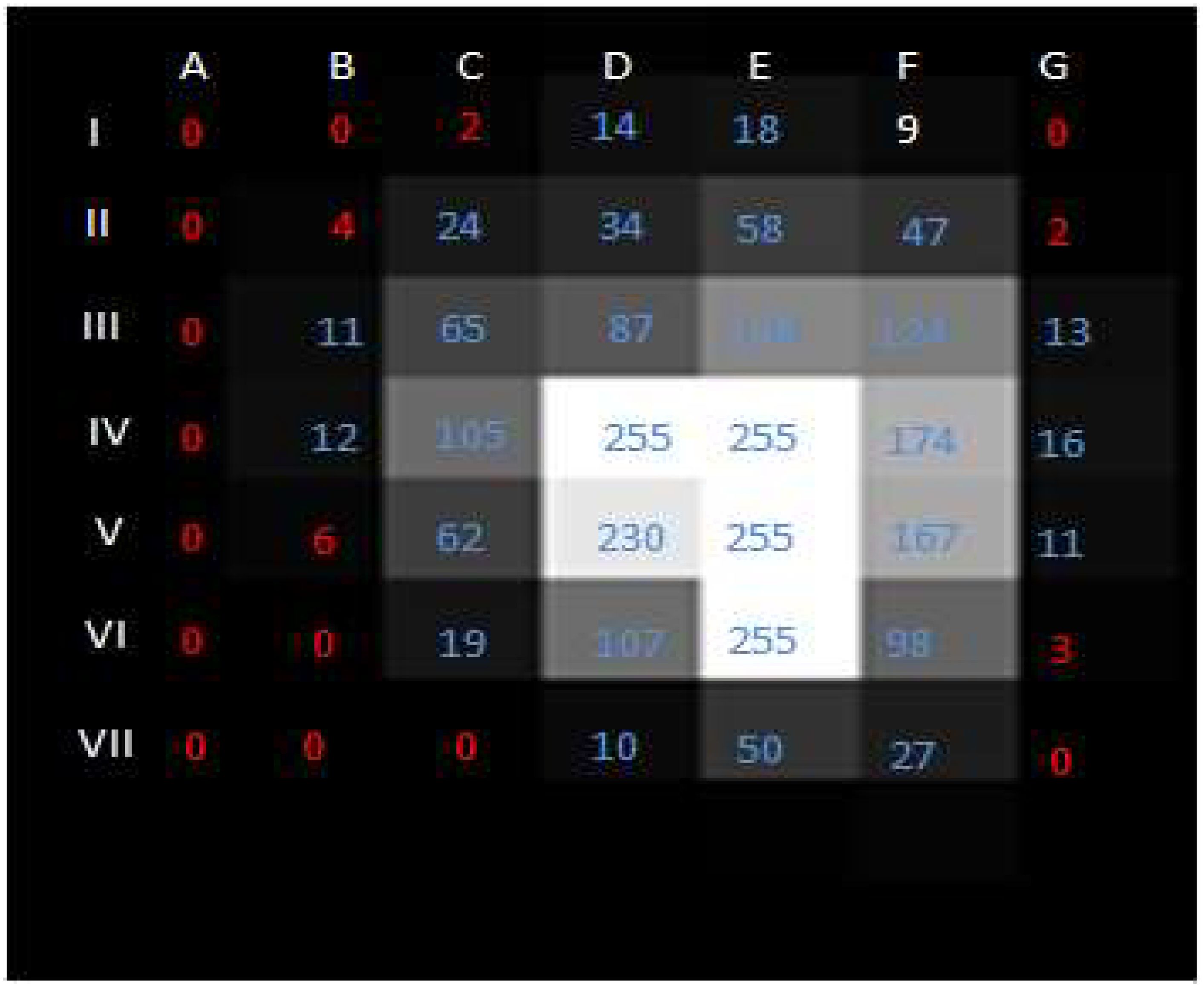
Figure 2 is an example representing each pixel of the gray intensity for the protrusion of height 280 μm on the black matrix (BM) layer.
In
Figure 2, the pixels in blue label the gray intensity of the effective pixels; whereas, the pixels in red are neglected because their gray level is lower than the threshold intensity and are not effective pixels. Furthermore, the height of the protrusion is converted to an equivalent diameter (
D) from square area to circular area by Equation (3), where
L is the length of the effective pixel,
k is the ratio between the area of a standard sample and the effective pixels’ area of a protrusion image. Its value depends on the protrusion types and light intensity. Hence, its value is determined beforehand using standard man-made defect samples of spheres of known diameter and light intensity. Namely, different
k values for different defects are used to determine the detective height more precisely.
The image resolution depends on the optical working distances (WD, the distance between the objective and focused surface) as seen in the thin-lens maker’s formula [
14]. A coarse optical resolution indicates a large magnification field of view. In geometrical optics, the proper optical resolution is shown in Equation (4) [
14]:
where
f is the focal point;
M is the magnification between the object and subject, and
represents the thickness of the lens. While scanning is performed, a signal capacitor array triggers the photon electronic current on the photoactive region. Each capacitor accumulates electron charges in proportion to the light intensity. Through signal amplification and decoding devices, the original signal is reconstructed by the shift register. Moreover, the standard deviation,
(sigma) calculated by Equation (5), is used to quantify the accuracy of the measurements; where
is the mean value of the dataset
, and
is the number of the samples.
In the end, the study utilizes side-view illumination to detect the protrusive defects and then transforms its effective pixels to calculate the equivalent diameter.
3. Experimental Architecture
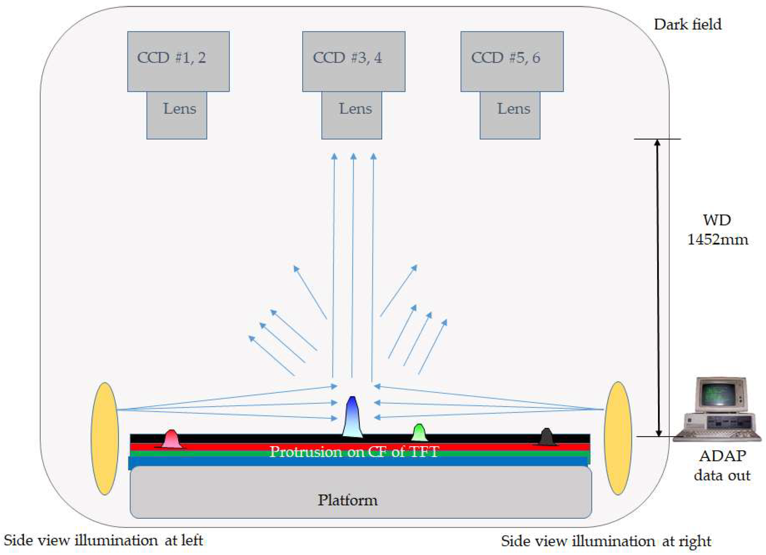
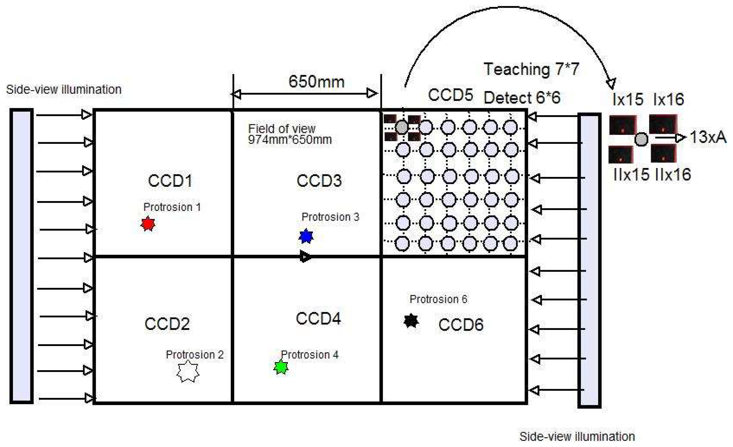
A schematic diagram of the side-view illumination protrusive detection system which connects an area CCD to detect the protrusion in the dark field is shown in
Figure 3. The system is installed on a flat platform on which two low-pressure sodium lights connected to the optical fibers are used to emit a set of parallel lights with the wavelength range covering more than the visual light. The tolerance of the platform is horizontally maintained at ±10 μm to ensure measurement accuracy. The platform accommodates the 6th generation TFT-LCD size of 1850 mm × 1500 mm. The optical system detecting area can be adjusted by the capability of the CCDs selected, including the whole field of view. The optical working distance from the substrate to the lens (focal length 50-mm, f/2.8) is 1452 mm. The parameters of the geometrical optics are tabulated in
Table 1.
The photosensor is a 30 fps, regular 8-bit, 256-grayscale, commercial off-the-shelf industrial area CCD with 4872 × 3248 pixels; the field of view is 650 mm × 974 mm (length × width). An automatic data acquisition program (ADAP) is used to obtain the height of the specific protrusion. The selected light spectrum is from 490 nm to 1050 nm so that the ultraviolet spectra are filtered out to avoid overexposure of the substrate. Typically, when the substrate is loaded to the platform in-line, the image is captured by the area CCD through the automatic data acquisition program. Then, the data output is performed automatically. The innovative method is fast, cost-effective, and reliable with 94% accuracy in the production line. Experiments are conducted in a 100-class clean room.
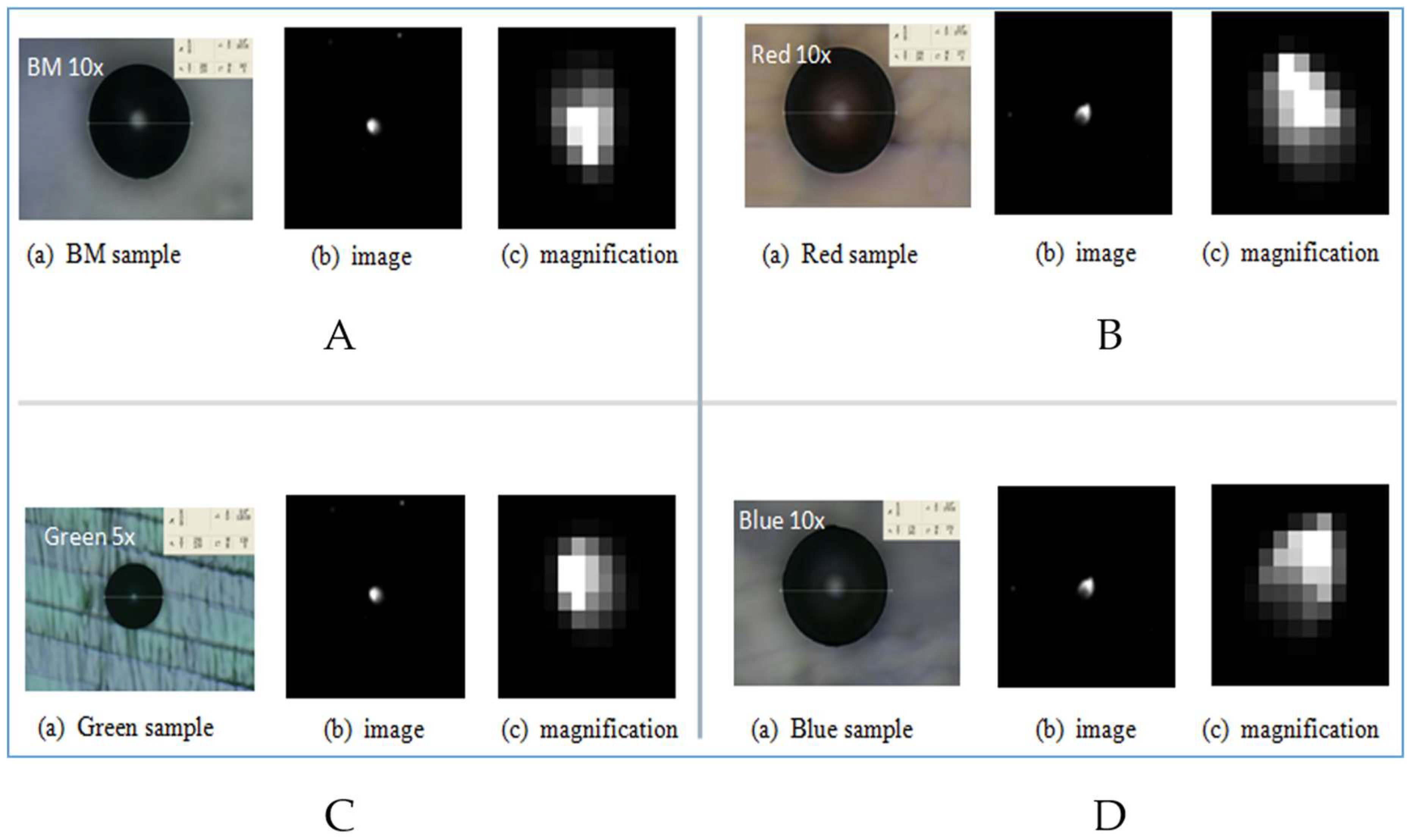
The protrusion defects are purposefully induced to test the present method. They are tailor-made samples of known diameters with individual thin-film of BM, red, green, and blue photoresists (PRs) coated around the glass ball.
4. Results and Discussion
Four kinds of samples are dispatched in various fields of view, in which the individual thin-film is uniformly coated on the glass by the black matrix (BM), and red, green, and blue photoresists (PRs), respectively. The corresponding diameters are 280, 277, 256, and 265 μm, as shown in
Figure 4 together with the associated image and image magnification. The sample receives the light from global directions; the sphere shape reflects even more light than that of other shapes. Coaxial light with the microscope is captured and measured and processed by Photoshop software.
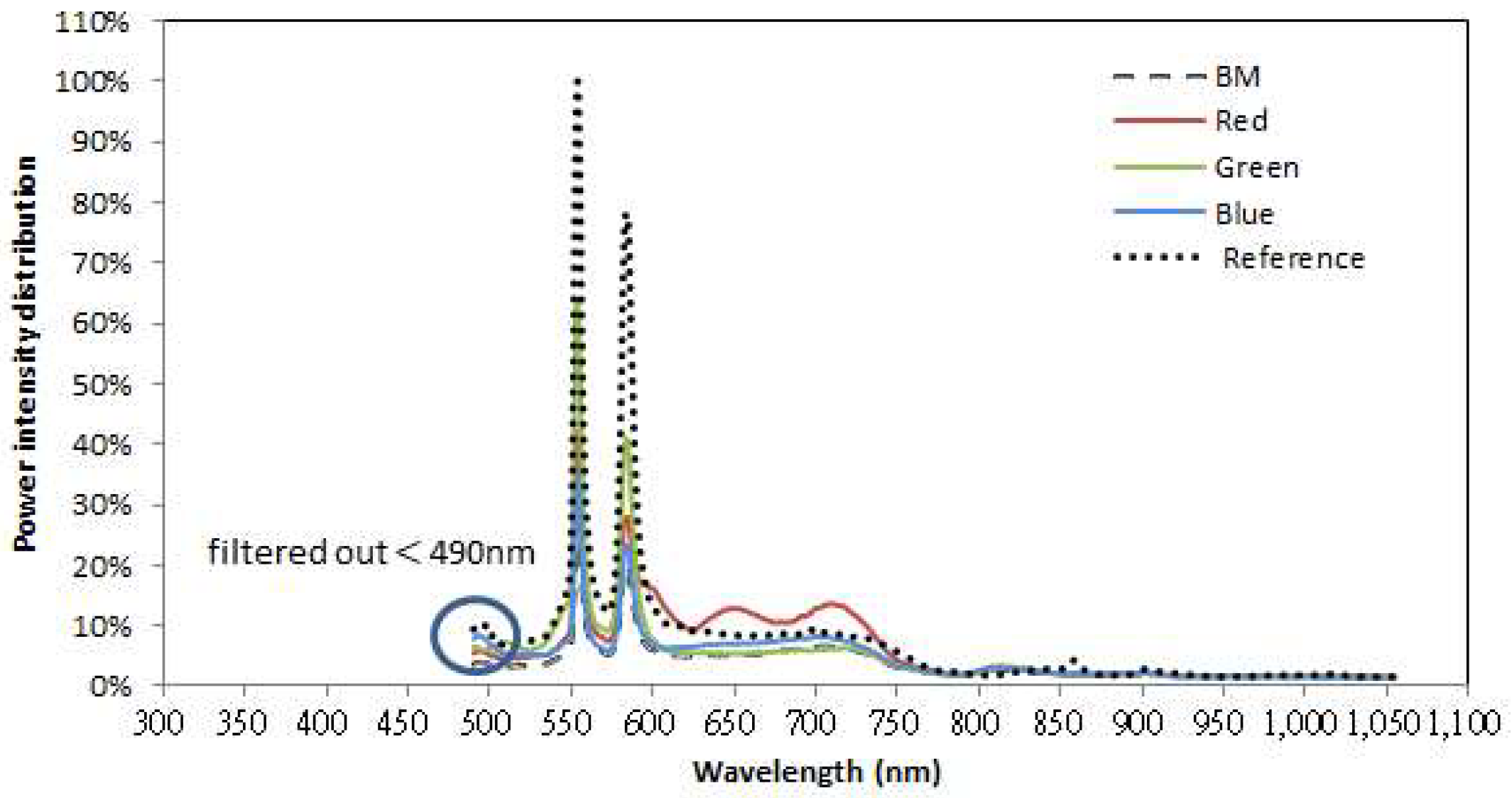
Figure 5 illustrates the spectra of these BM, red, green, and blue thin-films (referred to as films for simplicity), which are detected by a spectrometer with an optical resolution of 0.8 nm (BTC611E, back-thinned CCD array, working wavelength from 300 to 1050 nm, from B&W TEK, Newark, Delaware, USA). The light sources are 250 W low-pressure sodium lamps as their brightness can illuminate the whole region to be detected to satisfy the threshold of the gray level. However, the ultraviolet wavelength tends to deteriorate the quality of the PRs, causing color variation while the coater prints the color filter film in the process. Thus, a high-pass filter to reduce the wavelengths to smaller than 490 nm is to limit the spectral range from 490 to 1050 nm.
The optical characteristics of the glass with various films are shown in
Figure 5, exhibiting a lower reflection compared to that of reference air (free of film coating). For BM, the largest response is 26% at 550 nm; optical response at other wavelengths is below 10%. In contrast, the PRs demonstrate higher reflections, and the red film can shift energy between 600 and 750 nm. Thus, its reflective response is larger than the reference curve due to the red film characteristics.
Because the reflectivity depends on the individual sample configuration, the threshold of the gray level for each sample should be tuned accordingly so that more reliable measurement results can be obtained. Thus, the method of applying a set of
k ratios that correct the dark field for different samples was performed before the measurement was conducted. Moreover, the
k parameter, the area ratio between the sample area and the corresponding image area, depends on the standard sample height. Its value depends on the protrusion types and light intensity. Hence, its value is determined beforehand using standard man-made defect samples of spheres of known diameter and light intensity. Namely, different
k values for different defects are used to determine the detective height more precisely.
Figure 6 indicates that the
k ratio is a non-linear decay function of the height of protrusion from 100 to 300 μm. When the defect height increases, the effective area of its corresponding image also increases. Thus,
k decreases as the defect height increases due to the increased effective image area.
In this task, six CCDs are installed on the ceiling to cover all of the fields of view of the scan area. Before the protrusive height measurement is carried out, a neutralization technique using a matrix of a 7 × 7 (row × column) template for tuning is necessary, such as CCD#5 shown in
Figure 7. Therefore, six CCDs cover the 21 rows (1–21 row horizontally) and 14 columns (I–IVX in symbols vertically) of the matrices as shown in
Figure 7 [
1]. Furthermore,
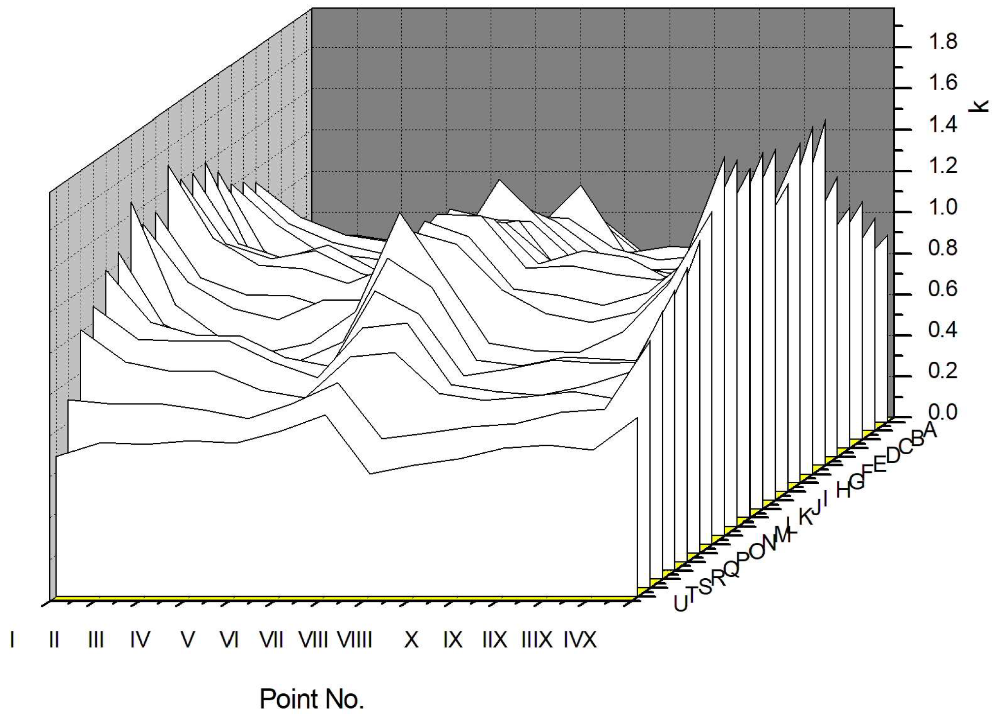
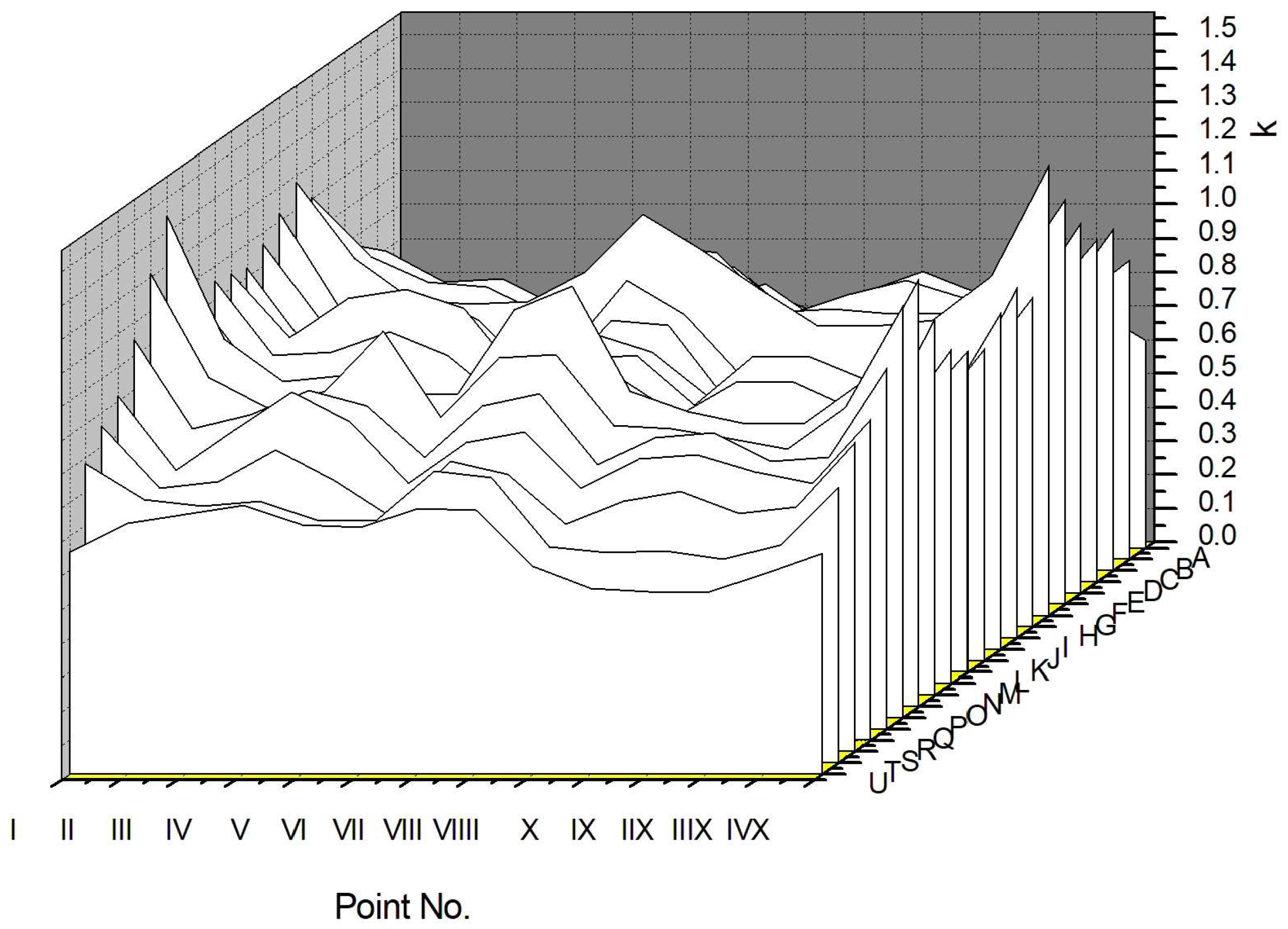
Figure 8 plots a 3D illustration of the profile of k where the x-axis is the front view (columns from I–IVX) of the engaged paired side-view illumination, emitting an incident light into the spatial field. As a result, the profile of k appears in a wave-form of W shape with respect to different rows (A–U). The area-CCDs installed on the top are in addition to the valley regions for detecting the protrusive defect. The triple-peaks of the regions indicates a large k ratio over the valley of W shape due to low reflection and weak albedo of BM. Moreover, smaller
k is found in regions of higher luminosity by the present side-view illumination method. Consequently, the region of low k versus high luminance is taken as the effective pixel. It can be noted that the BM thin-film is nearly a black-body that absorbs all of the incident light and results in a low albedo.
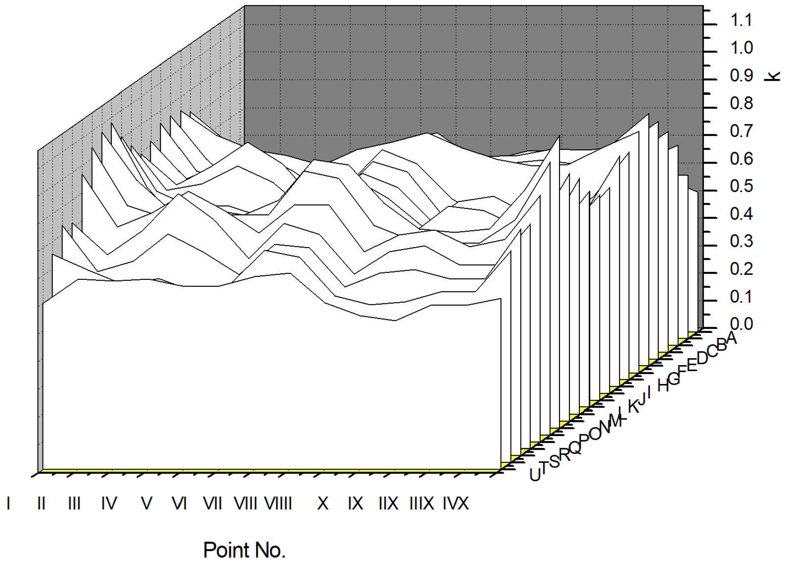
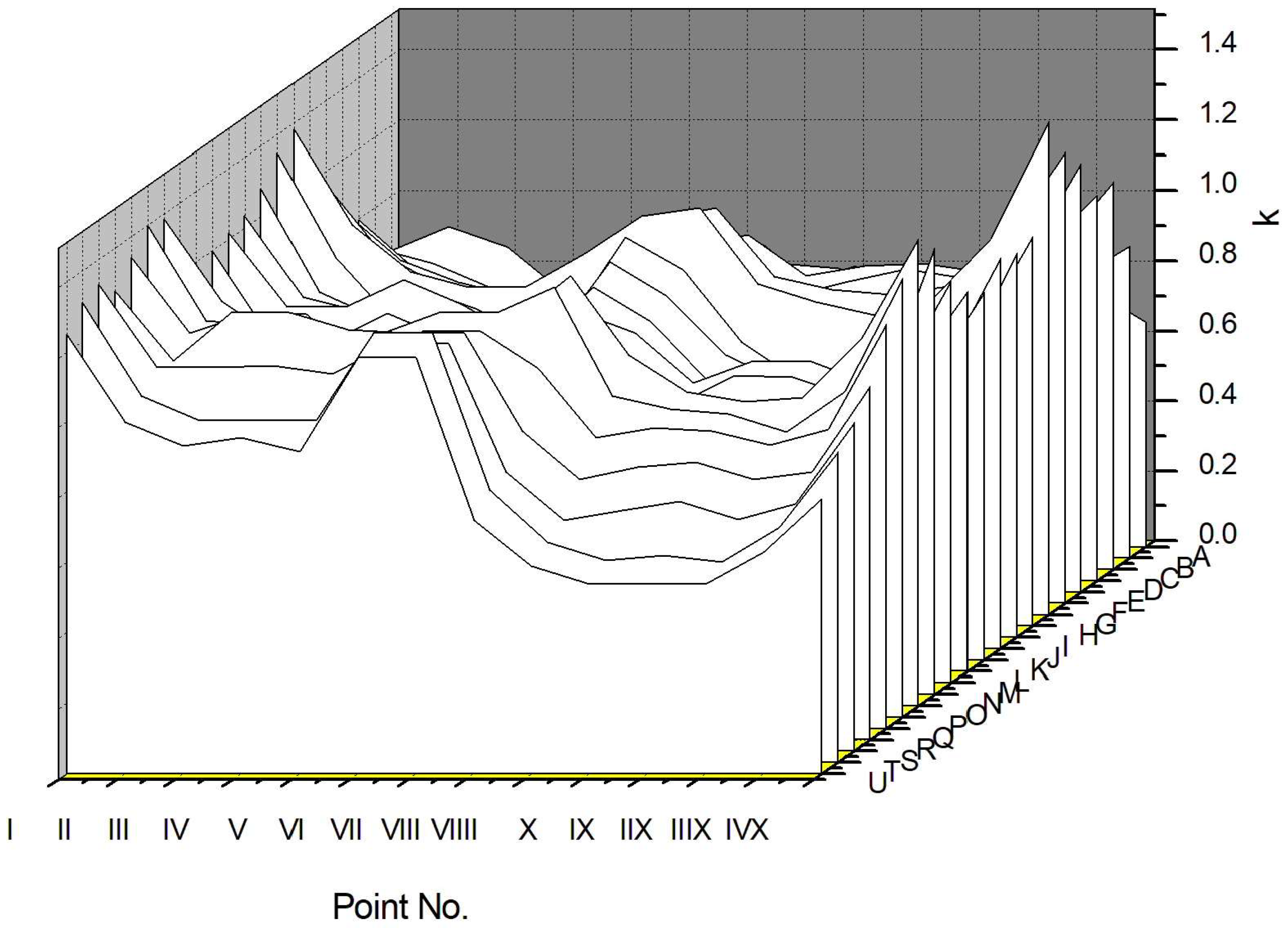
Figure 9,
Figure 10 and
Figure 11 show that smaller variations of k are found for the red, green, and blue films compared to that of BM, see
Figure 8. The highest value of k is around 1.0 and this occurred in the red film. The value of k was around 1.4 for the green film and around 1.4 of the blue film. Comparing these results to a k of over 1.6 for BM, it is evident that the value of k depends on the optical albedo and thus is used to tune the threshold.
The samples of known diameters, analogous to the protrusive defects, are placed on the test platform and are detected.
Table 2 shows the average height of 278 μm of 36 repeated measurements for the BM thin-film; the maximum height is 299 μm and the minimum is 262 μm. The error is from 6% to 7% with the uncertainty of three standard deviations being 25 μm.
Table 3,
Table 4 and
Table 5 illuminate the results of red, green, and blue thin-films, respectively; 36 repeated measurements were taken. For the red protrusion listed in
Table 3, the average measured height is 275 μm for the given height of 277 μm. The variation is from 283 to 266 μm. The error is from 2% to 4% with the three standard deviations of 13 μm. For the green defect, see
Table 4, the average height is 252 μm. The height variation is from 267 to 242 μm; the error is 8% to 5%, from maximum to minimum. For the blue film, see
Table 5, the average detected protrusive height is 262 μm (sample height of 265 μm). The height variation is from 274 to 254 μm. The error is 3% to 4%, from maximum to minimum.
As a result, because the sample of the BM thin-film has the lowest reflectivity compared to the red, green, and blue PRs, the BM thin-film results in the largest measurement error in terms of the three standard deviation measure 23 μm compared to those of the red thin-film 15 μm, the green thin-film 18 μm, and the blue thin-film 20 μm. Moreover, the maximum and minimum errors of BM are about 6% in contrast to the red, green, and blue thin-films of 3%–4%, 4%–6%, and 4%–6%, respectively. Thus, the colored thin-films have more correct measurement results than that of BM thin-film because colored thin-films exhibit stronger light intensity.


