Article

Study of Detector-Grade CdMnTe:In Crystals Obtained by a Multi-Step Post-Growth Annealing Method

1
School of Materials Science and Engineering, Chang’an University, Xi’an 710061, China
2
State Key Laboratory of Solidification Processing, Northwestern Polytechnical University, Xi’an 710072, China
*
Author to whom correspondence should be addressed.
Crystals 2018, 8(10), 387; https://doi.org/10.3390/cryst8100387
Submission received: 8 August 2018 / Revised: 5 October 2018 / Accepted: 7 October 2018 / Published: 11 October 2018

Abstract

:
A multi-step annealing method was successfully applied to inclusions reduction and resistivity improvement of CdMnTe:In (CMT:In) single crystals with high resistivity, including a Cd atmosphere annealing step followed by a Te atmosphere annealing step. After the Cd atmosphere annealing step, the density of Te inclusions was reduced distinctly, and it could be also decreased in the subsequent step of re-annealing under Te atmosphere. Both the resistivity and IR transmittance decreased notably after Cd atmosphere annealing, whereas they increased tremendously after re-annealing under a Te atmosphere. The reduction of full-width at-half-maximum (FWHM) and the increase of the intensity of the X-ray rocking curve indicated an improvement of the crystal quality. Meanwhile, after Cd atmosphere annealing, the increase of the intensity of the (D0,X) peak and the disappearance of the (A0,X) peak in photoluminescence (PL) measurements suggested further that the crystal quality was improved. The detector performance was enhanced obviously after annealing. The higher the annealing temperature, the better the performance was. The detector fabricated by CMT:In slice (Cd atmosphere annealing at 1073 K for 240 h and Te atmosphere re-annealing at 773 K for 120 h) with 9.43% energy resolution and 1.25 × 10⁻³ cm2/V μτ value had the best detector performance.

1. Introduction

The compound semiconductor material CdMnTe (CMT) has many applications for infrared (IR) detectors, solar cells, optical isolators and spintronic devices [1]. It is considered to be the substitute material of CdZnTe because of its optimal band-gap energy, fine mechanical stability, and near-unity segregation coefficient of Mn [2]. At present, CMT has attracted interest for the application of a room temperature radiation detector due to its wide band-gap, high resistivity, and good electron-transport properties [3,4,5]. However, CMT single crystals usually have some structure defects, especially Te inclusions, which will badly deteriorate the detector performance [6]. Therefore, in order to improve the crystal quality, researchers adopt post-growth annealing to reduce or eliminate these defects. However, few studies about the annealing of CMT crystals have been reported [7,8,9,10]. Generally, one annealing method only contains one step. For example, in order to reduce Te inclusions, CdTe-based crystals are generally annealed under a Cd atmosphere [11,12,13].
For CdTe-based room temperature radiation detectors, one very important property is resistivity. However, annealing in a Cd atmosphere will lead to an obvious decrease of the resistivity and the crystal will lose detection ability. How to increase the resistivity again is very important. As is well known, the Fermi-level of semiconductor material must be pinned at the mid band-gap position to obtain high resistivity. The deep-level centers in crystals are a key factor of obtaining high resistivity [14]. Moreover, the reduction of carrier concentration by Te annealing is another reason to obtain high resistivity. Yang et al. [15] used a two-step annealing method (Cd annealing followed by Te annealing) for CdZnTe. Te annealing results in abundant formation of Cd vacancies, which are acceptors, and then carrier concentration is decreased. In this paper, the aim is focused on the elimination of Te inclusions and keeping high-resistivity by optimal annealing conditions. The annealing of CMT:In crystals was adopted using a multi-step method, including a Cd atmosphere annealing step followed by a Te atmosphere annealing step. The effects of annealing temperature on the properties of CMT:In crystals were investigated. Moreover, the performance of CMT radiation detectors was also measured.

2. Materials and Methods

One Cd0.9Mn0.1Te:In (CMT:In) crystal ingot was grown using the modified vertical Bridgman method using high-purity raw materials of Cd (7N), Mn (5N), and Te (7N). The ingot was doped with 15 ppm Indium (7N), equivalent to a concentration of 5 × 10¹⁷ atoms/cm−3. CMT wafers were cut from the ingot along (111) face of the ingot. The wafers were then diced into small slices with the dimensions of 10 × 10 × 2 mm3. The slices with a resistivity of about 109 Ω·cm were chosen for multi-step annealing treatment. Annealing was performed in a two-zone furnace. Before annealing, all the slices were polished with MgO suspension and then etched with 3% Br2-MeOH solution. The multi-step annealing treatment was performed in two annealing steps, including a Cd atmosphere annealing step and a Te atmosphere annealing step. High-purity Cd (7N) and Te (7N) were used for the annealing sources. CMT could be considered as CdTe because of the low concentration of Mn in CMT. According to Li et al. [16], the annealing temperature must be chosen from 722 K to 1150 K. Thus, annealing temperatures of 1073 K, 973 K, and 873 K (higher than the melting point of Te (723 K)) were adopted for Cd atmosphere annealing. The annealing time was chosen as 240 h, according to our previous research [17]. The purpose of this step was to reduce or eliminate Te inclusions. The sources and the slices were fixed at different sides of quartz crucibles. The quartz crucibles were sealed under a vacuum of 10−5 Pa and then placed into a two-zone annealing furnace. When the annealing temperature on the side of the slice was 873 K, the temperature on the side of the source was 813 K. After annealing under a Cd atmosphere, the slices were re-annealed under a Te atmosphere. This step was aimed at enhancing the resistivity further. In order to reduce Cd evaporation in crystals, the annealing temperature of both slices and the source was chosen as 773 K. The annealing experiment under a Te atmosphere was also carried out in a two-zone furnace and the annealing time was 120 h.
The near-infrared spectrum (NIR) was tested by a Shimadzu UV-3150 UV-VIS-NIR spectrometer (Shimadzu, Tokyo, Japan) in the wavelength range of 1200 to 700 nm at room temperature. Te inclusions were observed by IR transmission microscopy (Micronviewer 7290A, Electrophysics Corporation, Fairfield, NJ, USA). IR transmittance was measured by a Nicolet Nexus 670 spectrometer (Thermo Electron Corporation, Waltham, MA, USA) in the wavenumber range from 4000 cm−1 to 500 cm−1. Photoluminescence (PL) measurement was carried out by a Triax 550 tri-grating monochrometer (HORIBA Jobin Yvon, Paris, France). An argon ion laser with a wavelength of 488 nm was used to excite the PL spectra. The measurement temperature was 10 K. Meanwhile, the current-voltage (I-V) curves of samples were tested by Agilent 4155C (Agilent Technologies Inc., Santa Clara, CA, USA) at room temperature. The energy resolution of the detectors was measured with an ORTEC measurement system (AMETEK ORTEC, Oak Ridge, TN, USA) using a 241Am γ-ray source.

3. Results and Discussion

3.1. Effect of Multi-Step Annealing on the Concentration of Mn

NIR transmittance is a nondestructive and easy way for determining the relative content of Mn and the band gap of CMT. The typical NIR transmittance spectra of CMT:In crystals before and after annealing (Cd atmosphere 1024 K/240 h, Te atmosphere 773 K/120 h) are shown in Figure 1. It can be seen that the shapes of the transmittance spectra of CMT:In crystals before and after annealing are almost coincident except for the maximum transmittance. This indicates that the multi-step, post-growth annealing has almost no effect on the Mn element because Mn vapor pressure is low. Therefore, the band gap of Cd0.9Mn0.1Te:In does not change before and after annealing.

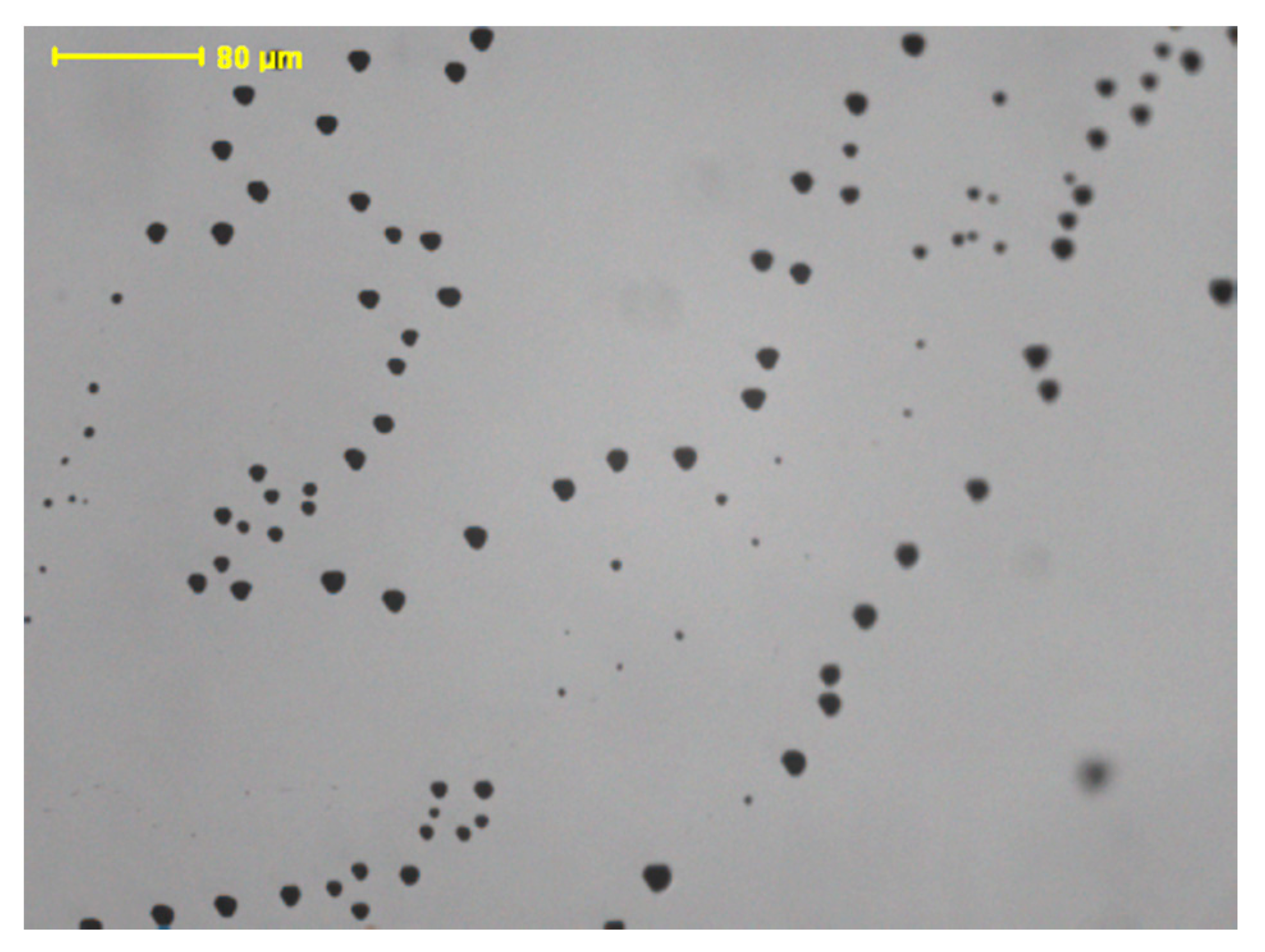
3.2. Effect of Multi-Step Annealing on Te Inclusions

Figure 2 shows the typical IR microscope image of Te inclusions in an as-grown CMT:In crystal. It can be observed that the density of Te inclusions is large. Te inclusions with the size about 1~15 μm are mainly near-triangular and hexagonal. Figure 3 shows IR microscope images of the CMT:In slices before and after annealing under a Cd atmosphere. The sample is observed in situ. For as-grown CMT:In slices (cut from the same wafer), the inclusion density is calculated to be (2~3) × 105 cm−2 (Figure 3A–C). After annealing at 873 K (Figure 3a), 973 K (Figure 3b), and 1073 K (Figure 3c), the densities of Te inclusions are reduced to the orders of 103 cm−2, 102 cm−2 and 101 cm−2. The density of Te inclusions markedly reduces when the thermal treatment temperature increases from 873 K to 1073 K. Apparently, annealing under a Cd atmosphere is effective for eliminating inclusions. Vydyanath et al. [18] pointed out that Te inclusions reduction could be explained by the thermomigration theory. When the thermal treatment temperature is higher than 723 K (the melting point of Te), the solid inclusion phase will transform to a liquid phase. The liquid inclusion phase migrates to the crystal surface and then will be eliminated by evaporation or reaction. Moreover, in this paper, Te inclusions cannot be eliminated completely when the temperature of annealing under Cd atmosphere is 1073 K and the time is more than 240 h. This result is consistent with that of our previous research [17]. According to the dynamics of thermal migration [19], Te inclusions with a small size were hard to migrate because of big surface energy. The size of some Te inclusions for CMT crystals investigated in this paper is only several microns or even about 1 μm. In the end, although the annealing takes a long time, these inclusions are still unable to be eliminated.
For clearly observing the morphology of the inclusions further, IR microscope images of the same CMT:In slice before and after Cd atmosphere annealing (873 K for 240 h) and Te atmosphere re-annealing (773 K for 120 h) are shown in Figure 4. In Figure 4A–C, the density of Te inclusions gradually decreases. However, the density is still in the order of 103 cm−2. In the enlarged images, the size of Te inclusions is smaller and smaller. Te inclusions can also be eliminated by annealing under Te atmosphere. A small number of Te inclusions still migrate when the annealing takes place under a Te atmosphere. The process is different from that of annealing under a Cd atmosphere. A Te atmosphere hinders the migration of Te inclusions, which results in few Te inclusions being eliminated. Moreover, the morphology of the inclusions is spherical after annealing. The reason is that Te droplets form during annealing and then the shape is maintained during cooling [20].

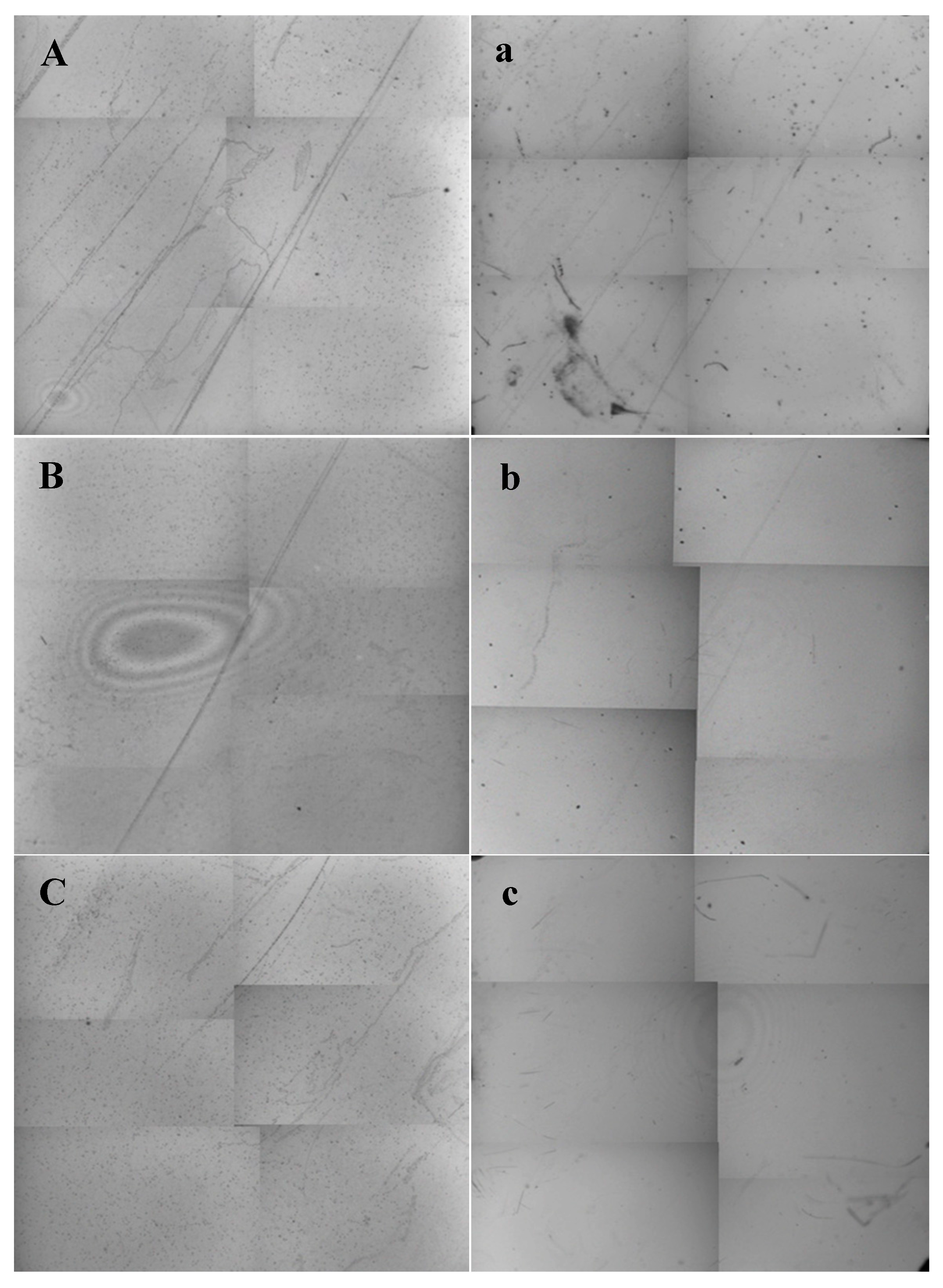
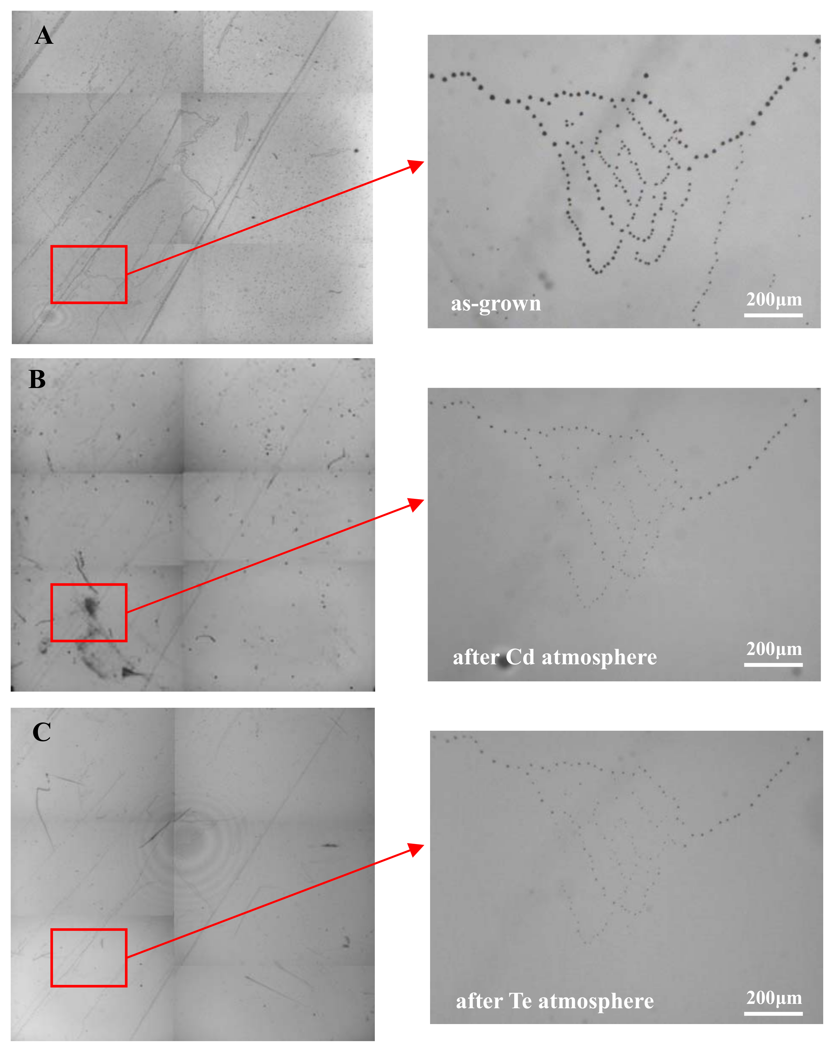
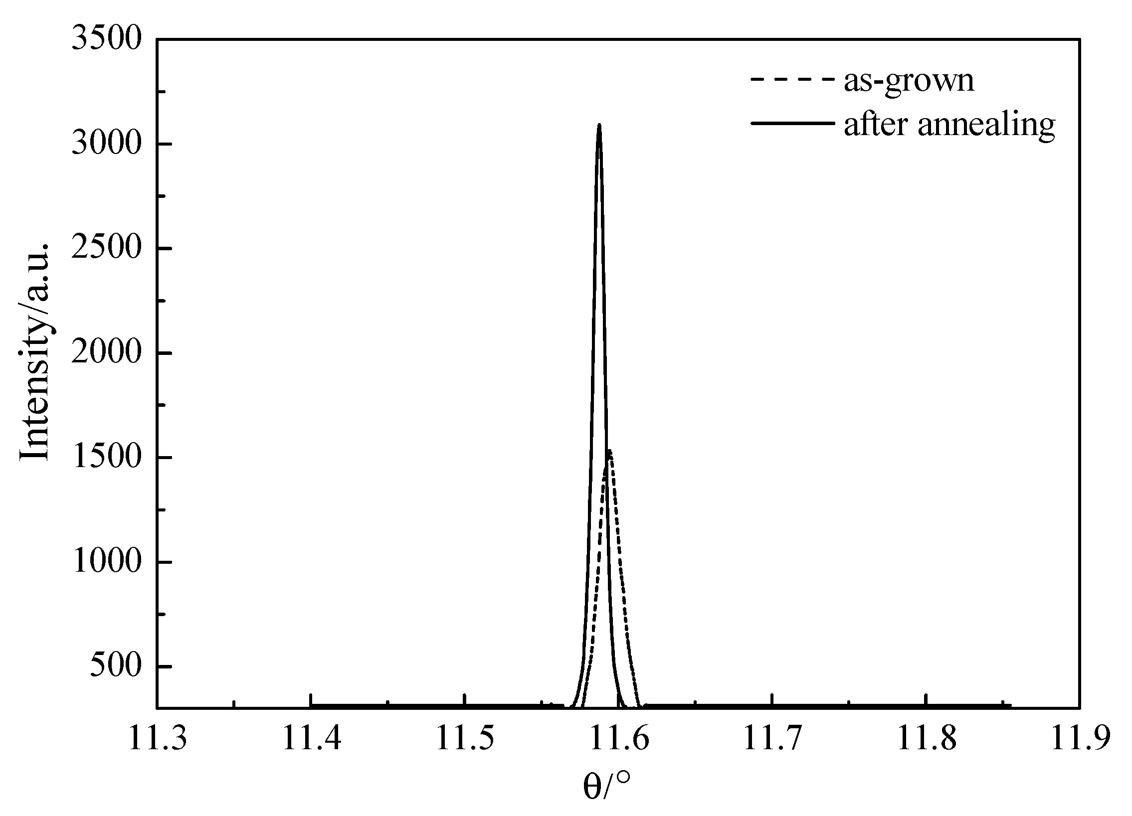
3.3. Effect of Multi-Step Annealing on Crystal Quality

An X-ray rocking curve is used to test the crystal quality of CMT before and after annealing, as shown in Figure 5. The result of the full-width at-half-maximum (FWHM) for the as-grown CMT:In crystal is 68″. Then, the value for the crystal after annealing decreases to 37″. Moreover, the corresponding intensity of the diffraction peak improves, and the position moves from 11.5945° to 11.5875°. Obviously, the result of the X-ray rocking curve indicates that the crystal quality is improved after annealing. Generally, the defect or macro elastic stress in crystals will destroy crystal structure perfection and cause the irregular array of atoms. In consequence, the crystal plane distorts and inclines, which results in the change of interplanar spacing. Thus, structure defects, such as inclusions and dislocations, will cause lattice distortion and the change of interplanar spacing. In this paper, many Te inclusions and dislocations exist in the as-grown crystal. These defects cause mismatch stress and destroy crystal structure. According to the Bragg’s law [17], the diffraction angle of an X-ray changes and the diffraction peak deviates from the theoretical position. The FWHM is wide and the intensity is weak. For the annealed crystal with fewer defects, the FWHM becomes narrow, the intensity is enhanced, and the diffraction peak moves closer to the theoretical position.

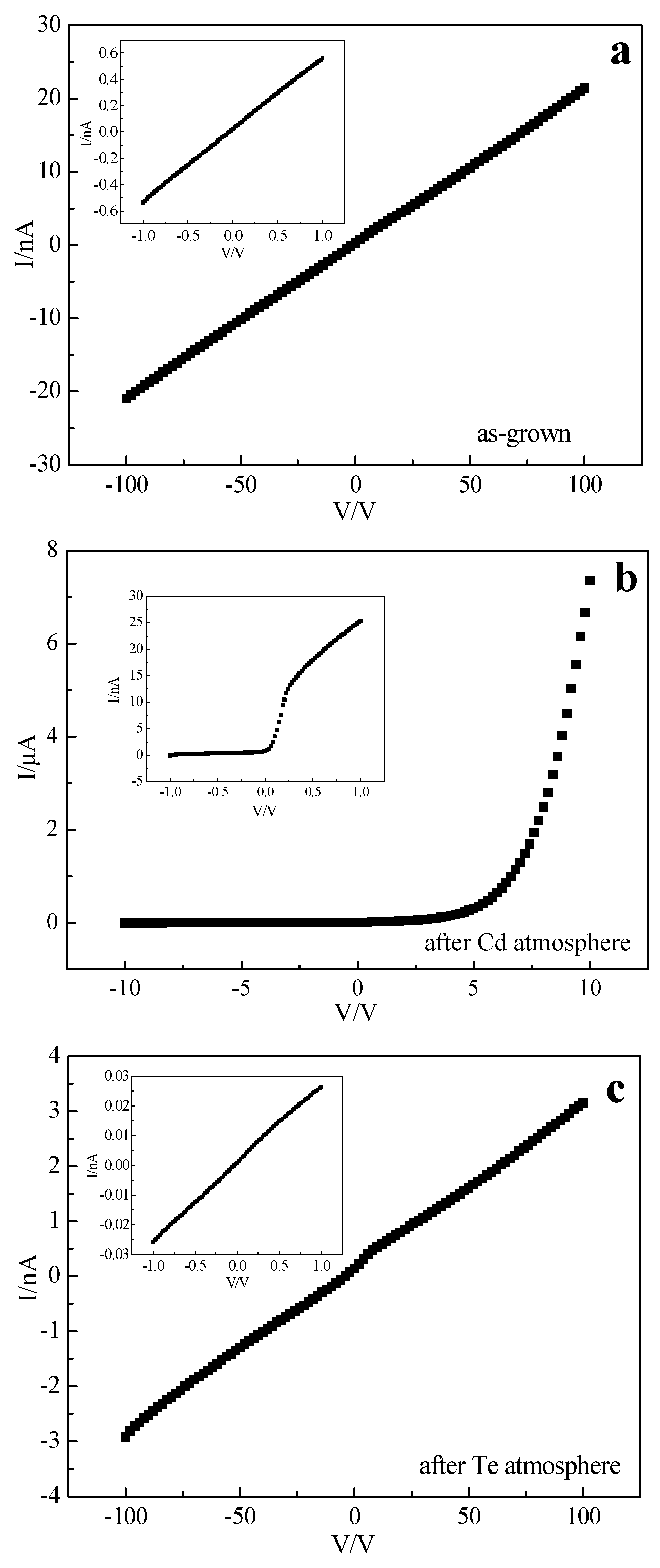
3.4. Effect of Multi-Step Annealing on Resistivity

For current-voltage (I-V) measurement, Au electrodes are deposited on both sides of the slices. Figure 6 shows the results of I-V measurements for CMT:In slices before and after annealing. The resistivity for as-grown CMT:In crystal is about 109 Ω·cm order of magnitude. The leakage current is within 21 nA when the bias voltage is 100 V. After annealing under a Cd atmosphere, the variation of the leakage current is noticeable (Figure 6b). A significant decrease of the resistivity is observed. When bias voltage is higher than 5 V, the leakage current rapidly increases and reaches up to μA order of magnitudes. Hall measurement indicates that the crystal exhibits n-type conduction. Lyahovitskaya et al. [21] pointed out that the concentration of electrons increased after Cd atmosphere annealing and resulted in n-type conduction. Actually, Cd atoms diffuse into CMT:In crystal to form Cd interstitial atoms (Cdi) during Cd-rich annealing. Thus, Cd vacancies (VCd) are wiped out. The concentration of the n-type carrier increases and material becomes n-type conduction. In Figure 6b, the I-V curve is nonsymmetrical. In fact, Cd will diffuse to both sides of CMT crystal, but more Cd atoms will diffuse to the side that is close to the Cd source, which will result in asymmetry of the I-V curve. For a long annealing time, Cd atoms will diffuse to the whole crystal and the I-V curve will be symmetrical. When bias voltage is higher than 50 V, the leakage current is large and reaches the limit of the equipment. After re-annealing under Te atmosphere, the resistivity is enhanced markedly (Figure 6c). This result achieves the purpose of keeping high resistivity. It can be seen that the leakage current is only 3 nA. The high-resistivity material is formed. Te saturated vapor pressure restrains the evaporation of the Te element in CMT crystal. Cdi atoms decrease and VCd-acceptor concentration is increased by the evaporation of the Cd element. Hall measurement indicates that the carrier concentration of the annealed CMT:In slice is 104 cm−3 order of magnitudes and the slice has weak p-type conduction. Therefore, the reduction of the carrier concentration results in high resistivity. The resistivities of 873 K, 973 K, and 1073 K in annealed CMT:In crystals are calculated to be 1.26 × 10¹⁰ Ω·cm, 2.24 × 10¹⁰ Ω·cm and 2.75 × 10¹⁰ Ω·cm, respectively, which are higher than that of as-grown crystals.

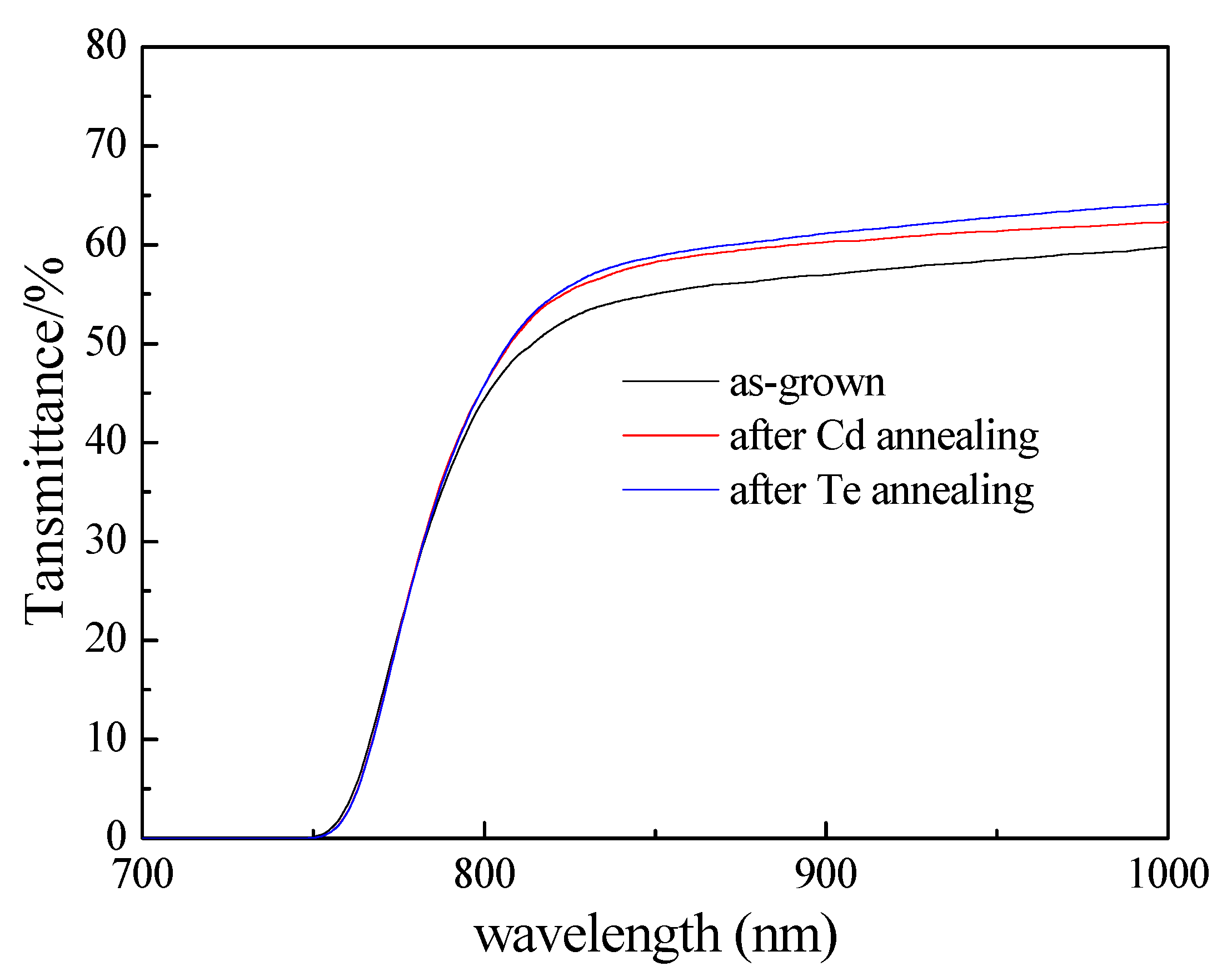
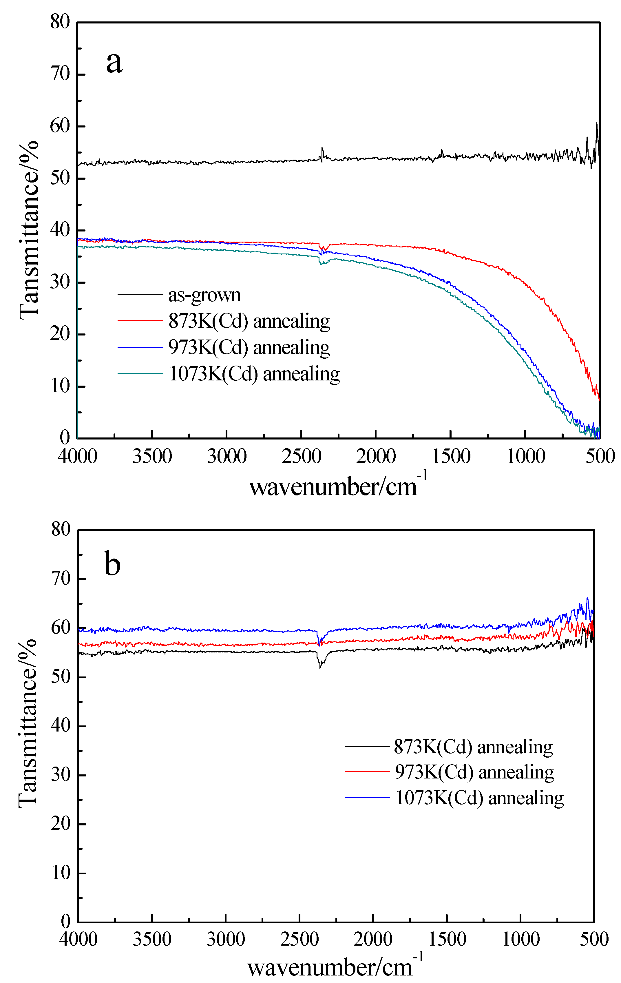
3.5. Effect of Multi-Step Annealing on IR Transmittance Spectra

IR transmittance spectrum is also used to evaluate the crystal quality of CMT crystals. Figure 7 shows the test result. In Figure 7a, the transmittance curves are high straight lines for both as-grown and annealed CMT:In slices in the wave number region from 500 cm−1 to 4000 cm−1. The average transmittance for as-grown crystal is 53%. However, the transmittance curves for Cd atmosphere annealed crystals show ascending lines. The average transmittances are 33% (873 K), 29% (973 K) and 27% (1073 K), respectively. Hall measurement indicates that the carrier concentration for as-grown crystals is 3.16 × 106 cm−3. However, the concentration of carriers for the crystal after Cd atmosphere annealing at 1073 K is 6.44 × 1014 cm−3. The carrier concentration increases tremendously. The higher the annealing temperature, the more the concentration of carriers there is. Here, the free-carrier absorption dominates the IR absorption and influences IR transmittance [22,23]. This result is consistent with that of electrical measurement after Cd atmosphere annealing.
In Figure 7b, the transmittance curves of the CMT:In slices show the feature of high straight lines again after re-annealing under Te atmosphere. Hall measurement indicates that the carrier concentration is 5.68 × 104 cm−3. It is clear that the carrier concentration is greatly decreased. The result is still consistent with that of electrical measurement after Te atmosphere annealing. The free-carrier absorption does not dominate the IR absorption because the carrier concentrations are low for all slices.

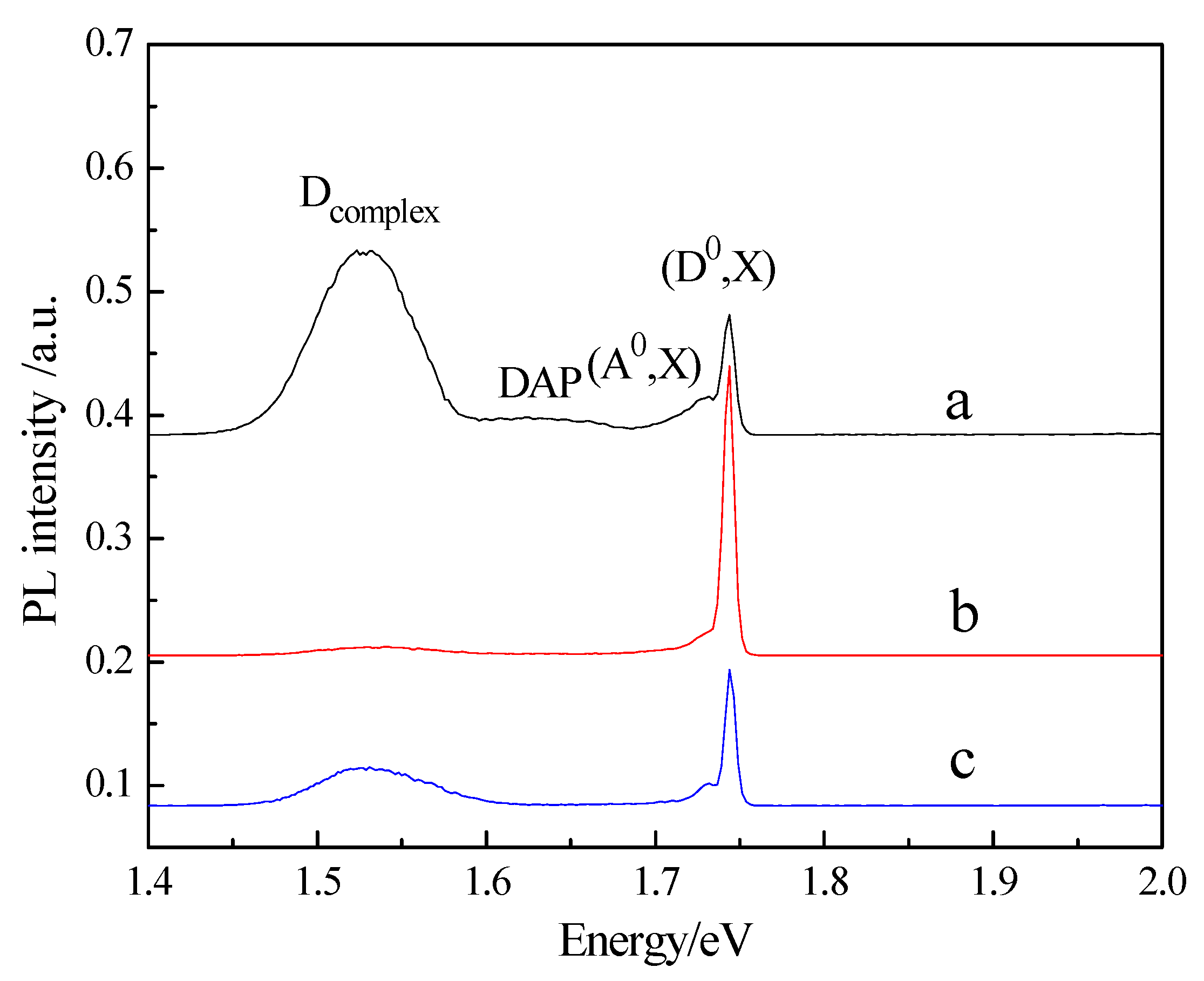
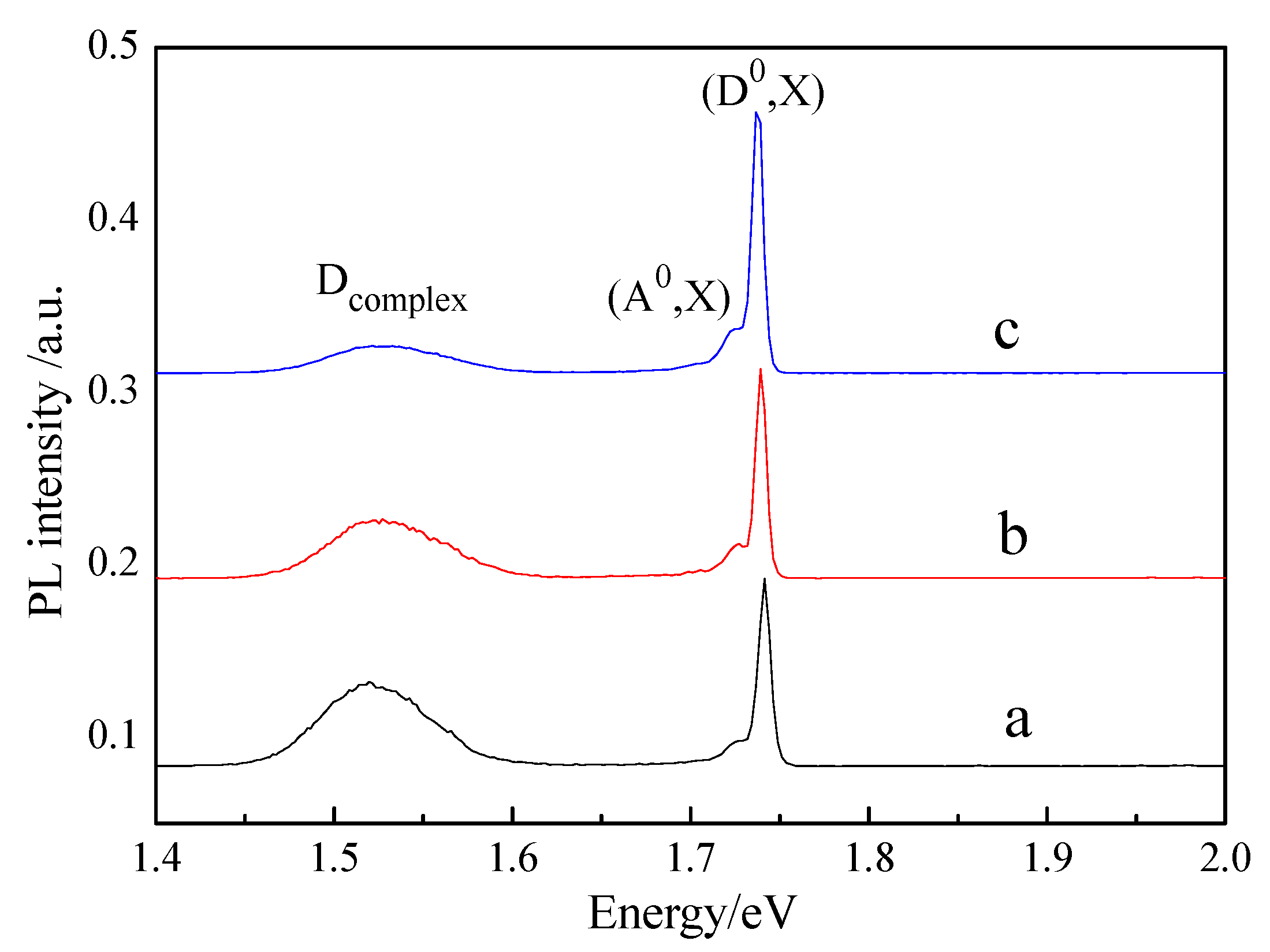
3.6. Effect of Multi-Step Annealing on PL Spectra

Photoluminescence (PL) spectroscopy is used to characterize point defects in CMT:In crystals. It is helpful to understand the annealing influence. The low-temperature PL spectra at 10 K for as-grown and annealed CMT:In slices is shown in Figure 8. The spectra can be divided into three regions according to Du et al. [22]. They are near-band-edge region (1.68–1.76 eV), donor-acceptor pair (D,A) region (1.59–1.68 eV), and A-center region (1.42–1.59 eV).
Comparing curve a with curve b in Figure 8, some interesting changes are found. In the near-band-edge region, the (A0,X) peak almost disappears after Cd atmosphere annealing. The intensity of the (D0,X) peak significantly increases and the FWHM reduces. Generally, the crystal quality depends on the intensity of the neutral donor bound exciton peak (D0,X). Cd atmosphere annealing effectively eliminates Te inclusions and improves the crystal quality. In the donor-acceptor pair (DAP) region, a DAP peak can be observed in as-grown crystal, while it disappears after annealing. The phenomenon can be explained by the removal of the impurities [17,22]. Moreover, the DAP peak is relative to the complexes formed by indium and Cd vacancy [24]. Cd atoms diffuse into CMT:In crystals and compensate Cd vacancies in the complexes. This can also decrease the intensity of the DAP peak. Finally, in the A-center region, the intensity of the Dcomplex peak remarkably decreases after annealing. A Dcomplex peak is generally ascribed to Cd vacancy-shallow donor complex [22]. In indium-doped CdTe-based crystals, ionized donor [InCd]+ and Cd vacancy related complex is responsible for the Dcomplex peak [25]. Two factors, the compensation of Cd vacancies and the elimination of Te inclusions, result in the reduction of the intensity of the Dcomplex peak. In addition, a I(D0,X)/I(Dcomplex) ratio is also adopted to evaluate the crystal quality. The larger the ratio, the better the crystal quality is. The ratios for as-grown and annealed crystals are 1.27 and 4.70, respectively. It also shows the improvement of the crystal quality. After re-annealing under Te atmosphere, comparing curve b with curve c in Figure 8, there are two obvious changes. First, the intensity of the (D0,X) peak decreases, and second the Dcomplex peak increases. It can be explained by the increase of Cd vacancy density in the process of Te atmosphere annealing [22]. After Te atmosphere annealing, the I(D0,X)/I(Dcomplex) ratio varies from 4.70 to 1.69. However, on the whole, the crystal quality is improved after annealing. Figure 9 shows the PL spectra of CMT:In crystals after multi-step annealing. It can be seen that the intensity of the (D0,X) peak increases and the intensity of the Dcomplex peak decreases as the annealing temperature increases. The corresponding value of the I(D0,X)/I(Dcomplex) ratios is also enlarged. Thus, the crystal quality is gradually improved with the increasing annealing temperature.

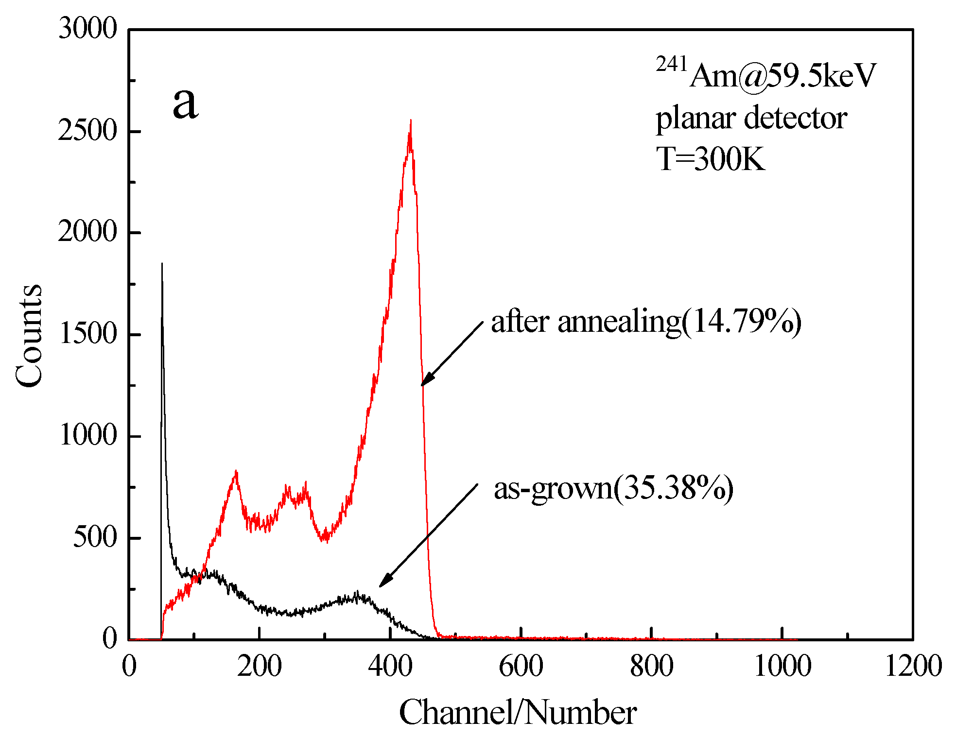
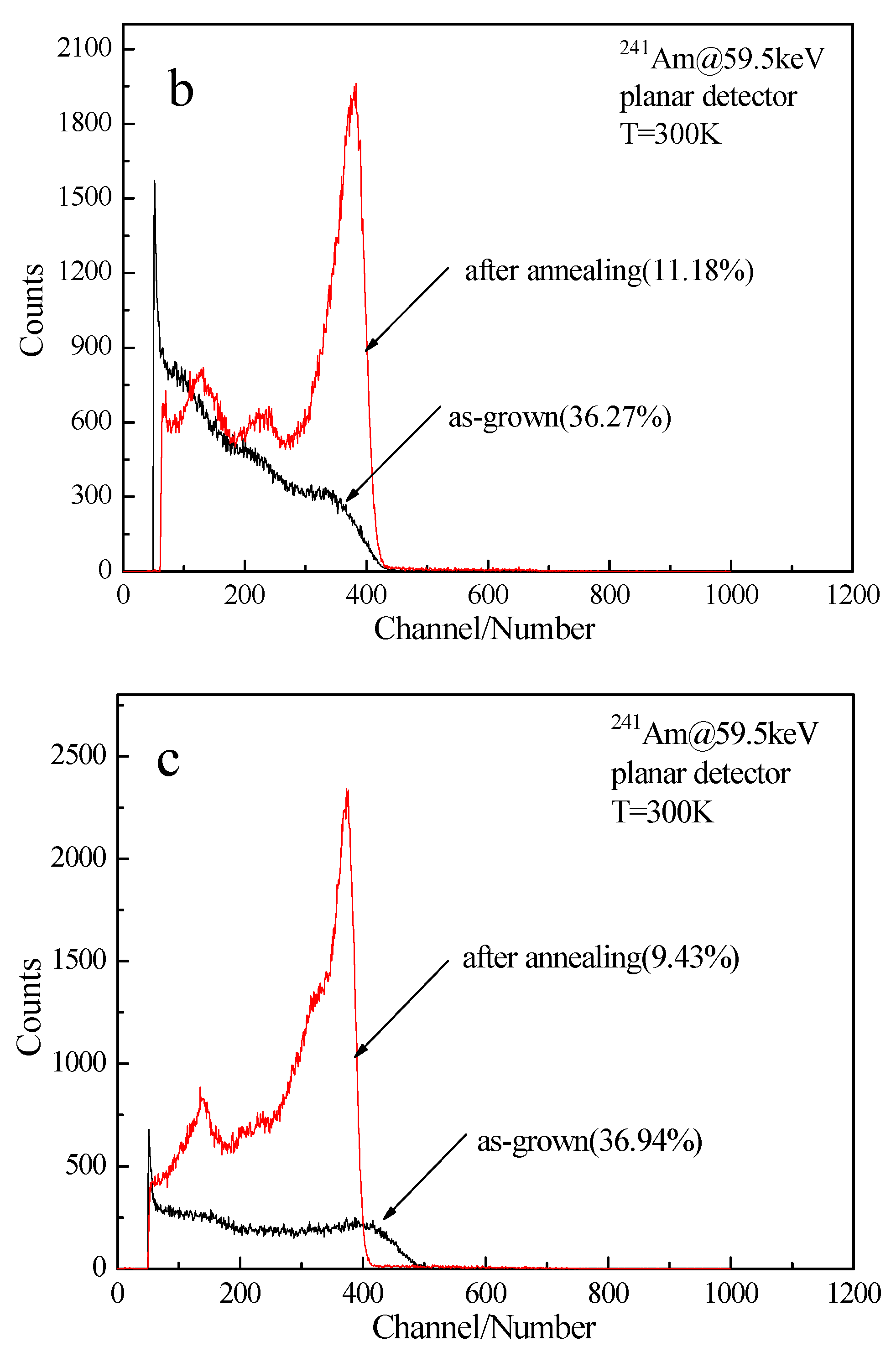
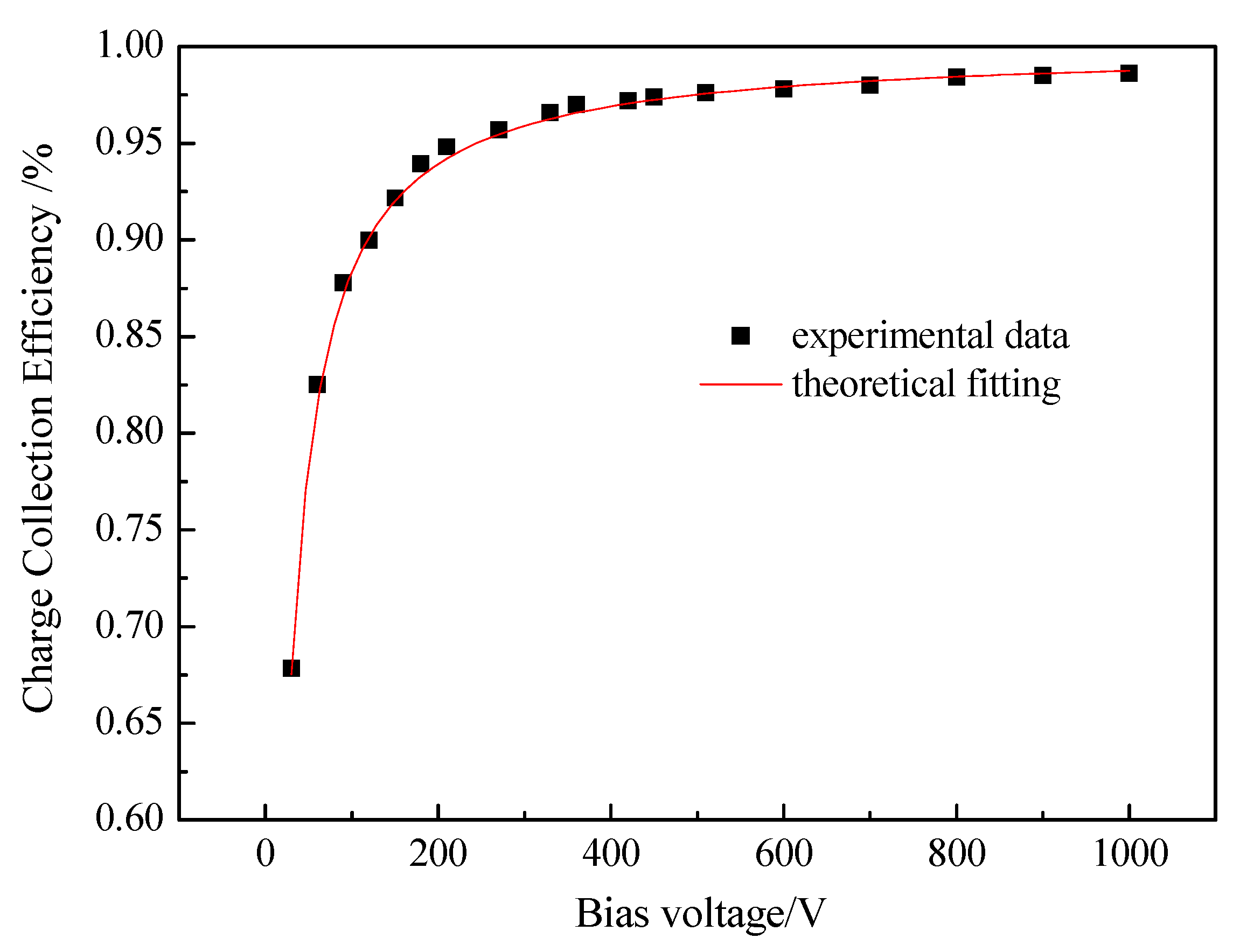
3.7. Effect of Multi-Step Annealing on the Performance of Detectors

The as-grown and annealed CMT:In slices are fabricated to room temperature detectors after the preparation of planar-electrodes on both sides. Figure 10 shows 241Am γ-ray spectra of the detectors. The applied voltage is 60 V, the shaping time is 1 μs. The energy resolutions of the detectors fabricated by three as-grown CMT:In slices are 35.38% (Figure 10a), 36.27% (Figure 10b) and 36.94% (Figure 10c), respectively. Meanwhile, the corresponding energy resolutions of the detectors fabricated by annealed CMT:In slices are 14.79% (Figure 10a), 11.18% (Figure 10b) and 9.43% (Figure 10c), respectively. Apparently, the energy resolution is drastically improved.
The Hecht Equation (1) [26] is used to calculate the mobility-lifetime products of single carriers (electron or hole), as follows:
Q = Q 0 × μ τ E d [ 1 exp ( d μ τ E ) ] ,
where Q and Q0 are the charge collection and the maximum collectible charge, respectively; μτ is the mobility-lifetime product; E is the applied electric field, and d is the thickness of the sample. As the voltage changes, the energy resolution and the position of the energy peak are also changed. Based on this, the collection efficiency of the detectors is determined. Then the μτ value for single carriers can also be calculated. The defects which are trapping centers will influence the mobility-lifetime product. For as-grown crystal, there are lots of Te inclusions and dislocations. Low resistivity will result in high leakage current, which causes high electrical noise. Therefore, the detectors fabricated by as-grown crystals have low collection efficiency and poor energy resolution. Thus, the μτ value of an electron for as-grown crystal cannot be calculated because there is not enough data of the voltage vs the peak position. After annealing, the defects are observably decreased and the resistivity is enhanced. As a consequence, the energy resolution improves. The collection efficiency of the detector (fabricated by the slice after Cd atmosphere annealing at 1073 K for 240 h and Te atmosphere re-annealed at 773 K for 120 h) at different voltages is shown in Figure 11. The μτ values of the detectors fabricated by annealed CMT:In slices are 2.50 × 10⁻⁴ cm2/V (873 K, Figure 10a), 7.58 × 10⁻⁴ cm2/V (973 K, Figure 10b) and 1.25 × 10⁻³ cm2/V (1073 K, Figure 10c), respectively. The detector with the best performance can achieve the requirement of high-performance detection. It is found that the mobility-lifetime product for as-grown CMT is about 10−3 cm2/V orders of magnitude [27], significantly less than that (about 10−2 cm2/V order of magnitudes) for as-grown CdZnTe [28]. There are mainly two reasons for this problem. First, the purity of Mn (5N) is markedly lower than that of Zn (7N). Second, CMT crystal with sphalerite structure has very low layer fault energy, which will result in the formation of more twins. Thus, more impurities and defects in as-grown CMT crystals reduce the mobility-lifetime product. Bulk CdZnTe with a high quality can be grown by high quality seeds. However, CMT seeds with a high quality are difficult to obtain. Moreover, compared to CdZnTe, the detector performance of the crystals obtained by post-growth annealing is also not good because CMT has more defects. In our previous work [29], Te inclusions could be eliminated completely for CdZnTe, but this defect could not be eliminated completely for CMT [30]. The best fitting for the μτ value is shown in Figure 11. However, there are still errors between the experimental and the theoretical values. It is known that the mobility-lifetime products are mainly influenced by defects. Defects, such as Te inclusions, will cause an inhomogeneous distribution of electric field. The migration of carriers will be influenced, which results in the deviation between the experimental and the theoretical values. Actually, the improvement of the detector performance is due to the enhancement of the crystal quality. The decrease of trapping centers improves the transmission efficiency of carriers, and high resistivity guarantees good energy resolution. The optimal annealing condition for CMT:In crystal is Cd atmosphere annealing at 1073 K for 240 h and re-annealing under Te atmosphere at 773 K for 120 h.

4. Conclusions

The main effects of a multi-step annealing method on secondary phase particles, related defects, and resistivity of high-resistivity CMT:In crystals were investigated. The method included a Cd atmosphere annealing step and a Te atmosphere annealing step. After annealing under a Cd atmosphere, most Te inclusions were eliminated. Re-annealing under a Te atmosphere could also reduce this defect. The decrease of the FWHM of an X-ray rocking curve and the increase of IR transmittance indicated the improvement of the crystal quality. PL measurements also showed that the crystal quality was improved by the increase of the intensity of the (D0,X) peak, the disappearance of the DAP peak and the decrease of the Dcomplex peak. After annealing, the detector performance was obviously improved. The higher the annealing temperature, the better the performance was. The best detector performance was a 9.43% energy resolution and a 1.25 × 10⁻³ cm2/V μτ value. The optimal condition of thermal treatment in this paper was Cd atmosphere annealing at 1073 K for 240 h and re-annealing under Te atmosphere at 773 K for 120 h.

Author Contributions

Analysis and writing, P.Y.; experiments and characterization, Y.C., W.L. (Wei Li), W.L. (Wenfei Liu), B.L., J.Y. and K.N.; project administration, W.J.; conceptualization and methodology, L.L., J.Z., Z.L., M.B., G.S., and H.L.

Funding

This research was funded by the National Natural Science Foundations of China (Grant Nos. 51602026, 51608041, 21607013 and 11604022), the Natural Science Basic Research Plan in Shaanxi Province of China (No. 2018JM5150), the China Postdoctoral Science Foundation (Grant No. 2014M550509), the Special Fund for Basic Scientific Research of Central Colleges of Chang’an University (Nos. 300102318106, 300102318202, 310831171014), and Undergraduate Training Programs for Innovation and Entrepreneurship of Chang’an University (No. 201710710274).

Conflicts of Interest

The authors declare no conflicts of interest.

References

  1. Parkin, J.; Sellin, P.J.; Davies, A.W.; Lohstroh, A.; Özsan, M.E.; Seller, P. α Particle response of undoped CdMnTe. Nucl. Instrum. Meth. A 2007, 573, 220–223. [Google Scholar] [CrossRef]
  2. Hossain, A.; Cui, Y.; Bolltnikov, A.E.; Camarda, G.S.; Yang, G.; Kochanowska, D.; Witkowska-baran, M.; Mycielski, A.; James, R.B. Vanadium-doped cadmium manganese telluride (Cd1−xMnxTe) crystals as x- and gamma-ray detectors. J. Electron. Mater. 2009, 38, 1593–1599. [Google Scholar] [CrossRef]
  3. Roy, U.N.; Camarda, G.S.; Cui, Y.; Gu, G.; Gul, R.; Hossain, A.; Yang, G.; Egarievwe, S.U.; James, R.B. Growth and characterization of CdMnTe by the vertical Bridgman technique. J. Cryst. Growth 2016, 437, 53–58. [Google Scholar] [CrossRef] [Green Version]
  4. Babalola, O.S.; Bolotnikov, A.E.; Groza, M.; Hossain, A.; Egarievwe, S.; James, R.B.; Burger, A. Study of Te inclusions in CdMnTe crystals for nuclear detector applications. J. Cryst. Growth 2009, 311, 3702–3707. [Google Scholar] [CrossRef]
  5. Du, Y.Y.; Jie, W.Q.; Zheng, X.; Wang, T.; Bai, X.X.; Yu, H. Growth interface of In-doped CdMnTe from Te solution with vertical Bridgman method under ACRT technique. Trans. Nonferrous Met. Soc. China 2012, 22, s143–s147. [Google Scholar] [CrossRef]
  6. Hossain, A.; Gu, G.D.; Bolltnikov, A.E.; Camarda, G.S.; Cui, Y.; Yang, G.; Roy, U.N.; Yang, G.; Liu, T.; Zhong, R.; et al. Material and detector properties of cadmium manganese telluride (Cd1−xMnxTe) crystals grown by the modified floating-zone method. Nucl. Instrum. Meth. A 2015, 784, 33–36. [Google Scholar] [CrossRef]
  7. Kochanowska, D.; Mycielski, A.; Witkowska-Baran, M.; Szadkowski, A.; Witkowska, B.; Kaliszek, W.; Cui, Y.; James, R.B. Influence of annealing on tellurium precipitates in (Cd,Mn)Te:V crystals. IEEE Nucl. Sci. Symp. Conf. Rec. 2009, NSS’08, 202–206. [Google Scholar]
  8. Zhang, J.J.; Wang, L.J.; Min, J.H.; Qin, K.F.; Huang, J.; Tang, K.; Liang, X.Y.; Shen, P. Annealing of indium-doped CdMnTe single crystals under Cd vapors. J. Cryst. Growth 2012, 358, 12–15. [Google Scholar] [CrossRef]
  9. Zhang, J.J.; Wang, L.J.; Min, J.H.; Qin, K.F.; Shi, Z.B.; Liang, X.Y. Te vapor annealing of indium-doped CdMnTe crystals. J. Semicond. 2015, 34, 033002. [Google Scholar] [CrossRef]
  10. Adams, A.L.; Agbalagba, E.O.; Jow, J.O.; Mwathi, J.G.; Egarievwe, A.A.; Chan, W.; Dowdell, M.C.; Roy, U.N.; Egarievwe, S.U. Thermal annealing of CdMnTe material being developed for nuclear radiation detection applications. IOSR J. Mech. Civil Eng. 2016, 14, 1–5. [Google Scholar] [CrossRef]
  11. Bugár, M.; Belas, E.; Procházka, J.; Hlídek, P.; Grill, R.; Franc, J.; Höschl, P. IR transmittance of CdTe after high-temperature annealing. Nucl. Instrum. Meth. A 2011, 633, S83–S85. [Google Scholar] [CrossRef]
  12. Kim, K.; Bolotnikov, A.E.; Camarda, G.S.; Hossain, A.; James, R.B. Overcoming Zn segregation in CdZnTe with the temperature gradient annealing. J. Cryst. Growth 2016, 442, 98–101. [Google Scholar] [CrossRef] [Green Version]
  13. Egarievwe, S.U.; Yang, G.; Egarievwe, A.A.; Okwechime, I.O.; Gray, J.; Hales, Z.M.; Hossain, A.; Camarda, G.S.; Bolotnikov, A.E.; James, R.B. Post-growth annealing of Bridgman-grown CdZnTe and CdMnTe crystals for room-temperature nuclear radiation detectors. Nucl. Instrum. Meth. A 2015, 784, 51–55. [Google Scholar] [CrossRef] [Green Version]
  14. Chu, M.; Terterian, S.; Ting, D.; Wang, C.C.; Dinan, J.H.; James, R.B.; Burger, A. Effects of excess tellurium on the properties of CdZnTe radiation detectors. J. Electron. Mater. 2003, 32, 779–782. [Google Scholar] [CrossRef]
  15. Yang, G.; Bolotnikov, A.E.; Fochuk, P.M.; Kopach, O.; Franc, J.; Belas, E.; Kim, K.H.; Camarda, G.S.; Hossain, A.; Cui, Y.; et al. Post-growth thermal annealing study of CdZnTe for developing room-temperature X-ray and gamma-ray detectors. J. Cryst. Growth 2013, 379, 16–20. [Google Scholar] [CrossRef]
  16. Li, G.Q.; Zhang, X.L.; Jie, W.Q.; Hui, C. Thermal treatment of detector-grade CdZnTe. J. Cryst. Growth 2006, 295, 31–35. [Google Scholar] [CrossRef]
  17. Yu, P.F.; Xu, Y.D.; Luan, L.J.; Du, Y.Y.; Zheng, J.H.; Li, H.; Jie, W.Q. Quality improvement of CdMnTe:In single crystals by an effective post- growth annealing. J. Cryst. Growth 2016, 451, 194–199. [Google Scholar] [CrossRef]
  18. Vydyanath, H.R.; Ellsworth, J.A.; Parkinson, J.B.; Kennedy, J.J.; Dean, B.; Johnson, C.J.; Neugebauer, G.T.; Sepich, J.; Liao, P. Thermomigration of Te precipitates and improvement of (Cd,Zn)Te substrate characteristics for the fabrication of LWIR (Hg, Cd)Te photodiodes. J. Electron. Mater. 1993, 22, 1073–1080. [Google Scholar] [CrossRef]
  19. Anthony, T.R.; Cline, H.E. Thermal migration of liquid droplets through solids. J. Appl. Phys. 1971, 42, 3380–3387. [Google Scholar] [CrossRef]
  20. Yu, P.F.; Jie, W.Q. Observation, morphology evolution and elimination of Te inclusions in CdZnTe:In single crystals. J. Cryst. Growth 2013, 381, 57–60. [Google Scholar] [CrossRef]
  21. Lyahovitskaya, V.; Chernyak, L.; Greenberg, J.; Kaplan, L.; Cahen, D. n- And p-type post-growth self-doping of CdTe single crystals. J. Cryst. Growth 2000, 214, 1155–1157. [Google Scholar] [CrossRef]
  22. Du, Y.Y.; Jie, W.Q.; Wang, T.; Zheng, X.; Xu, Y.D.; Luan, L.J. Solution growth of In-doped CdMnTe crystals by the vertical Bridgman method with the ACRT technique. J. Cryst. Growth 2012, 355, 33–37. [Google Scholar] [CrossRef]
  23. Yu, P.F.; Luan, L.J.; Du, Y.Y.; Zheng, J.H.; Jie, W.Q. Investigation of Te atmosphere annealing on the properties of detector-grade CdMnTe:In single crystals. J. Cryst. Growth 2015, 430, 103–107. [Google Scholar] [CrossRef]
  24. Zhang, J.J.; Wang, L.J.; Min, J.H.; Huang, J.; Liang, X.Y.; Tang, K.; Shen, P.; Shen, M.; Liang, W.; Huang, N.S.; Xia, Y.B. Characterization of CdMnTe crystal grown with vertical Bridgman method under Te-rich conditions. Phys. Status Solidi C 2014, 11, 1174–1177. [Google Scholar] [CrossRef]
  25. Li, Q.; Jie, W.Q.; Fu, L.; Wang, T.; Yang, G.; Bai, X.X.; Zha, G.Q. Optical and electrical properties of indium-doped Cd0.9Zn0.1Te crystal. J. Cryst. Growth 2006, 295, 124–128. [Google Scholar] [CrossRef]
  26. Jones, K.A.; Ciampi, G.; Skrip, C.E.; Lynn, K.G. Vertical Bridgman growth of Cd1-xZnxTe for room temperature radiation detectors. Proc. SPIE 2007, 6706, 670607. [Google Scholar]
  27. Kim, K.; Jeng, G.; Kim, P.; Choi, J.; Bolotnikov, A.E.; Camarda, G.S.; James, R.B. Influence of the cooling scheme on the performance and presence of carrier traps for CdMnTe detectors. J. Appl. Phys. 2013, 114, 063706. [Google Scholar] [CrossRef]
  28. Chen, H.; Awadalla, S.A.; Iniewski, K.; Lu, P.H.; Harris, F.; Mackenzie, J.; Hasanen, T.; Chen, W.; Redden, R.; Bindley, G.; et al. Characterization of large cadmium zinc telluride crystals grown by traveling heater method. J. Appl. Phys. 2008, 103, 014903. [Google Scholar] [CrossRef] [Green Version]
  29. Yu, P.F.; Jie, W.Q. Effects of post-growth annealing on the performance of CdZnTe: In radiation detectors with different thickness. Nucl. Instrum. Meth. A 2014, 737, 29–32. [Google Scholar] [CrossRef]
  30. Yu, P.F.; Xu, Y.D.; Chen, Y.R.; Song, J.; Zhu, Y.; Zhang, M.J.; Zhang, B.G.; Wang, Y.; Li, W.; Luan, L.J.; et al. Investigation of effective annealing on CdMnTe:In crystals with different thickness for gamma-ray detectors. J. Cryst. Growth 2018, 483, 94–101. [Google Scholar] [CrossRef]
Figure 1. The typical near-infrared spectrum (NIR) transmittance spectra of CMT:In crystals before and after annealing (Cd atmosphere 1073K/240 h, Te atmosphere 773 K/120 h).
Crystals 08 00387 g001
Figure 2. The typical IR image of an as-grown CMT:In crystal.
Crystals 08 00387 g002
Figure 3. IR images of CMT:In crystals before and after Cd atmosphere annealing: (AC) as-grown; (a) 873 K for 240 h; (b) 973 K for 240 h; (c) 1073 K for 240 h. The size of the images is 9 × 9 mm2.
Crystals 08 00387 g003
Figure 4. IR images of CMT:In crystals before and after annealing: (A) as-grown; (B) after Cd atmosphere annealing at 873 K for 240 h; (C) after Te atmosphere annealing at 773 K for 120 h. The size of the images is 9 × 9 mm2.
Crystals 08 00387 g004
Figure 5. X-ray rocking curves of CMT:In slices, before and after annealing.
Crystals 08 00387 g005
Figure 6. Current-voltage (I-V) curves of CMT:In crystals before and after annealing: (a) as-grown; (b) after Cd atmosphere; (c) after Te atmosphere. The inserts are the I-V curves (−1V~1V) of the crystals.
Crystals 08 00387 g006
Figure 7. IR transmittance curves of CMT:In crystals before and after annealing: (a) Cd atmosphere; (b) Te atmosphere.
Crystals 08 00387 g007
Figure 8. Photoluminescence (PL) spectra of CMT:In crystals before and after annealing: (a) as-grown (b) Cd atmosphere; (c) Te atmosphere.
Crystals 08 00387 g008
Figure 9. PL spectra of CMT:In crystals after multi-step annealing: (a) Cd atmosphere annealing at 873 K and Te annealing re-annealing at 773 K; (b) Cd atmosphere annealing at 973 K and Te annealing re-annealing at 773 K; (c) Cd atmosphere annealing at 1073 K and Te annealing re-annealing at 773 K.
Crystals 08 00387 g009
Figure 10. 241Am γ-ray spectra of CMT detectors fabricated by as-grown and annealed CMT:In slices: (a) Cd atmosphere at 873 K for 240 h and Te atmosphere at 773 K for 120 h; (b) Cd atmosphere at 973 K for 240 h and Te atmosphere at 773 K for 120 h; (c) Cd atmosphere at 1073 K for 240 h and Te atmosphere at 773 K for 120 h.
Crystals 08 00387 g010aCrystals 08 00387 g010b
Figure 11. Collection efficiency of CMT:In detectors after Cd atmosphere annealing at 1073 K for 240 h and Te atmosphere re-annealing at 773 K for 120 h.
Crystals 08 00387 g011

