1. Introduction
Since the first demonstration of GaN-based light-emitting diodes (LEDs) in the early 1990s, there has been remarkable progress in GaN-based LEDs over the last two decades [
1,
2,
3,
4]. The efficiency of blue LEDs has been improved to a level that allows for the LED-based solid-state lighting to rapidly replace conventional light bulbs. The peak external quantum efficiency (EQE) of GaN-based blue LEDs has been reported to be higher than 80% [
5]. Despite such successful commercialization and technical advancement, there still remain some scientific issues limiting the efficiency of LEDs still remain. For example, the emission efficiency of blue LEDs decreases significantly with increasing injection current. This “efficiency droop” phenomenon results in limited light output power at high current densities [
6,
7,
8,
9]. In addition, the EQE of GaN-based yellow-green LEDs with emission wavelengths from 530 to 600 nm has been reported to be <30%, which has been termed the “green gap” problem [
10,
11,
12].
Recently, a GaN-based nanorod LED structure has drawn increasing attention as an alternative technology to overcome the efficiency limitation of current LED structures [
13,
14,
15,
16]. Nanorod structures have high potential to enhance the efficiency of LEDs significantly. In the core-shell nanorod LED structure, for example, high internal quantum efficiency is expected to be obtained as a result of reduced dislocation density and internal polarization fields [
14]. In addition, improvement in optical properties can also be expected from nanorod LED structures. First, light extraction efficiency (LEE) can be increaed greatly in the nanorod LED stuctures [
17,
18,
19]. Owing to the nano-scale geometry, light can easily escape from the nanorod overcoming the total internal reflection inside it. Second, spontaneous emission (SE) rate can be enhanced through the strong modifications of the optical density of states in the nanorod structure. It has been theoretically found that this Purcell effect can mitigate the efficiency droop and the green gap problems to some extent [
20,
21].
Such optical properties of a nanorod LED structure have been usually studied theoretically using numerical simulations based on the finite-difference time-domain (FDTD) method due to its complex geometry [
22,
23,
24]. In the FDTD method, a point dipole source is placed inside the nanorod structure and the evolution of electromagnetic fields is monitored, from which the LEE or the Purcell factor can be calculated. For the simulation of the planar LED structures, simulation with a single dipole source can give accurate results, irrespective of the source positions and polarization directions due to the translational symmetry in the plane of quantum wells. For the simulation of the nanorod LED structures, on the contrary, simulation results may differ from source positions and polarization directions because the translational symmetry is no longer maintained. However, in the most cases of FDTD simulation works on nanorod LEDs, simuilation results for only a single dipole source placed usually at the center of nanorod structures have been reported, which may provide incorrect information on the LEE, Purcell factors, and emission patterns of nanorod LEDs.
In this paper, we investigate the dependence of positions and polarization of a dipole source on the LEE and emission patterns of nanorod LED structures using FDTD simulations. The LEE of the nanorod LED is determined by averaging over the active area and the polarization directions, which is expected to provide reliable information for the LEE of the nanorod LED structure. The averaged LEE is calculated as the radius, the p-GaN thickness, and the n-GaN thickness is varied, and the optimum nanorod LED structure for high LEE is discussed. The far-field pattern (FFP) data from the nanorod LED are also presented by averaging the FFP over dipole source positions and polarization directions.
2. Simulation Methods
For the FDTD simulation of this work, a commercial program, FDTD Solutions by Lumerical Inc. was employed.
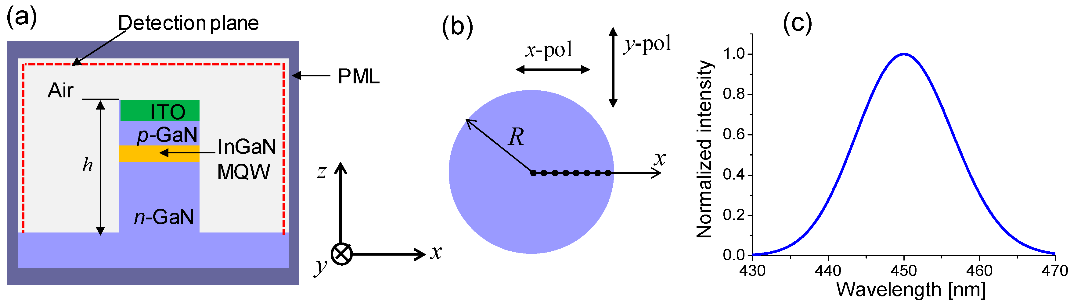
Figure 1a shows a schematic side view of the FDTD computational domain. A cylindrical nanorod LED structure with radius
R and height
h is formed on the n-GaN layer. The nanorod LED consists of the n-GaN layer, 10-nm InGaN/GaN multiple-quantum-well (MQW) active layers, a p-GaN layer, and a 100-nm indium-tin-oxide (ITO) layer for current injection. The simulated nanorod LED structure is not encapsulated and exposed to air. The refractive indices of GaN and ITO were set at 2.45 and 1.94 + 0.015
i, respectively [
25]. The InGaN/GaN active region is modeled as a uniform medium with the effective refractive index of 2.49. The dispersion was not considered in this simulation because the relative change of the refractive indices of GaN and ITO is less than 1% in the wavelength range from 440 to 460 nm. The perfectly matched layers (PMLs) were employed in all boundaries of the FDTD simulation domain. Propagating light waves are completely absorbed in the PML. The FFP and the Poynting vectors are calculated on the detection plane near PMLs that are shown as dotted line of the computational domain in
Figure 1a.
In the FDTD simulation, a single dipole source is positioned at the MQW active region in the
z-direction of
Figure 1a. The spectral intensity of the dipole source has a Gaussian shape in the frequency axis. As shown in
Figure 1c, the peak wavelength and full-width at half maximum of the spectrum are set to be 450 and 15 nm, respectively. The LEE at position (
x,
y) in the plane of QWs with polarization
p (
) is obtained when considering the spectral average of the source spectrum. That is,
where
is the LEE at position (
x,
y) and wavelength
λ with the polarization state
p and
is the spectral distribution shown in
Figure 1c.
The LEE (
η) averaged over the active area and two polarization directions can be obtained from
where
is the LEE at coordinates (
x,
y) with the polarization state
p. For each source position, there are two orthogonal polarization directions,
x-polarization and
y-polarization. That is, there are two polarization states for each source position.
Figure 1b shows the cross section of the nanorod LED structure. We assume that the simulated nanorod LED structures have circularly-shaped cross section. Solid dots inside the cross section represent the position of the dipole source in the
x-axis, with the interval of 25 nm. The two orthogonal polarization directions are also shown. Using the circular symmetry of the nanorod structure,
η is simplified as
where
is the LEE at
x with the polarization state
p. Equation (3) will give the accurate LEE value for nanorod LED structures with circular cross section.
3. Results and Discussion
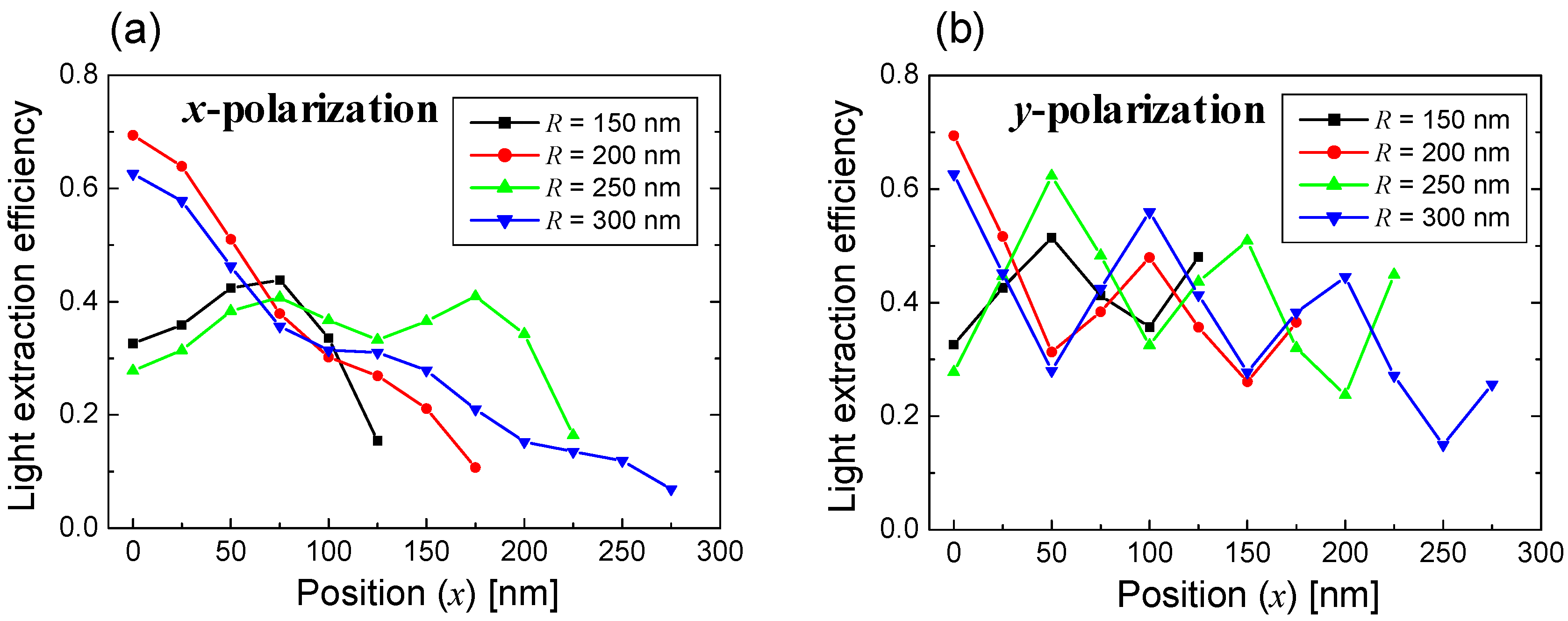
Figure 2 shows the LEE as a function of the source position in the
x direction for the rod radii of 150, 200, 250, and 300 nm. Strong dependence of the LEE on the source position and the polarization direction is observed. When the rod radius is 200 and 250 nm, the LEE shows a deceasing behavior with increasing source position although the LEE fluctuates with the variation of the source position. In this case, the LEE at the rod center can be higher than 60%. However, it decreases to ~20% when the source position is near the boundary of the nanorods. On the contrary, when the rod radius is 150 and 250 nm, the LEE at the rod center is relatively low and the LEE does not decrease much with an increasing source position.
This complicated dependence of the LEE on the source position, polarization, and the rod radius seems to be related with the resonant mode profiles inside the nanorod. In fact, there exist lots of resonant modes inside the nanorod cavity and each mode has a different optical loss or quality factor (
Q), which makes it difficult to analyze the LEE based on resonant mode properties. Nevertheless, the mode analysis is expected to provide insight into the behavior of the LEE.
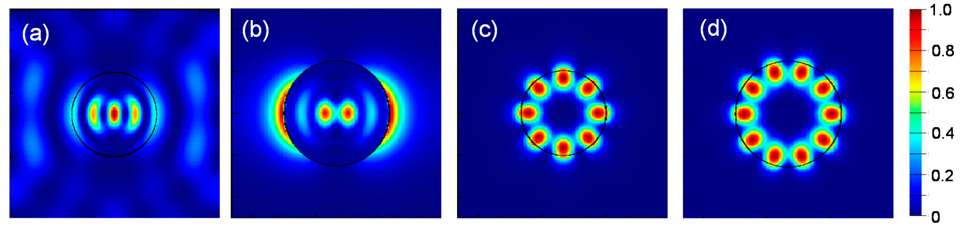
Figure 3 shows two-types of representative resonant mode profiles in the cross section of a nanorod structure for the rod radius of 200 and 250 nm.
Figure 3a,b show electric field intensity distribution of the radial modes (RMs) for rod radius of 200 and 250 nm, respectively.
Figure 3c,d show that of the whispering gallery modes (WGMs) for rod radius of 200 and 250 nm, respectively. The RM oscillates in the direction of rod diameter (
x-direction in
Figure 3a,b), and the light coupled with the RM can escape the nanorod structure relatively easily, resulting in a high LEE. On the contrary, the WGM oscillates along the circumference of the rod. The WGM generally has a very high
Q and appears as the lasing mode of a micro-disk laser [
26]. If a dipole source couples with the WGM, the emitted light travels along the circumference of the rod and escapes from the rod quite slowly, resulting in a low LEE. This can explain the decreasing behavior of the LEE with an increasing source position in
Figure 2.
When a dipole source is positioned near the rod center, it will couple to the RM rather than the WGM. As shown in
Figure 3a,b, the intensity at the center of the rod is high for the rod radius of 200 nm, whereas it is relatively low for the rod radius of 250 nm. Therefore, for the rod radius of 200 nm, the dipole source at the rod center couples well with the RM and a high LEE is expected. For the rod radius of 250 nm, on the contrary, the dipole source at the center does not couple well with the RM and the low LEE is expected. This interpretation can explain the different LEE values at the rod center for different rod radius. Since the RM oscillates in the
x-direction, it couples well with the dipole source of the
y-polarization when the dipole is not positioned at the center.
Figure 2b shows a periodic behavior of the LEE with increasing
x for the
y-polarization. The high (or low) LEE appears when the dipole position coincides with the high (or low) intensity of the RM profile. The periodicity of ~100 nm approximately corresponds to the antinode spacing of a standing wave pattern of the RM,
λ/2
n, where
n is the refractive index of GaN.
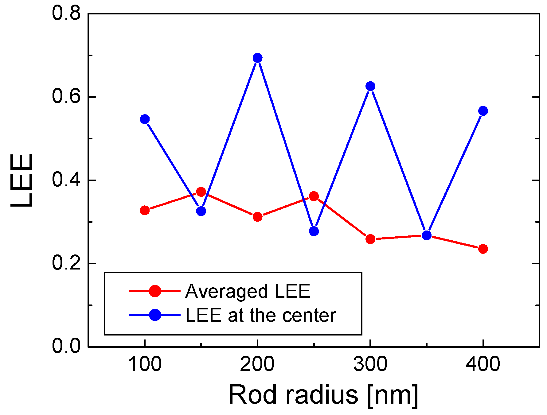
In
Figure 4, the averaged LEE defined in Equation (3) is plotted as a function of rod radius along with the LEE at the rod center. The LEE at the rod center changes sensitively with the rod radius. It can be higher than 60% when the rod radius is 200 and 300 nm. However, it decreases below 30% when the radius is 250 and 350 nm. This large variation is attributed to the strong dependence of resonant mode profiles at the rod center on the radius of the nanorod, as discussed before. The averaged LEE changes much stably with the rod radius as a result of the averaging effect. The local peak of the averaged LEE is observed at the rod radius of 150 and 250 nm. In this case, the averaged LEE is slightly higher than the LEE at the rod center. When the rod radius is 150 and 250 nm, the LEE at the center is low and the LEE at large
x is relatively less decreased. Since the contribution to the averaged LEE increases linearly with
x, as one can see from Equation (3), relatively high averaged LEE was obtained for the rod radius of 150 and 250 nm where the LEE at large
x is relatively high.
Up to now, most FDTD simulation results on nanorod LEDs have been based on the simuilation restuls with a single dipole source placed at the center of nanorod, as mentioned before. However, the results of
Figure 4 indicate that the LEE performed with a dipole source at the rod center differs quite significantly with the LEE averaged over source positions and polarization directions, implying that the simulation with only one dipole source may provide incorrect information on the LEE. For example, LEE at the rod center has its peak at the rod radius of 200 and 300 nm, whereas the averaged LEE results indicate the optimum rod radius is 150 or 250 nm.
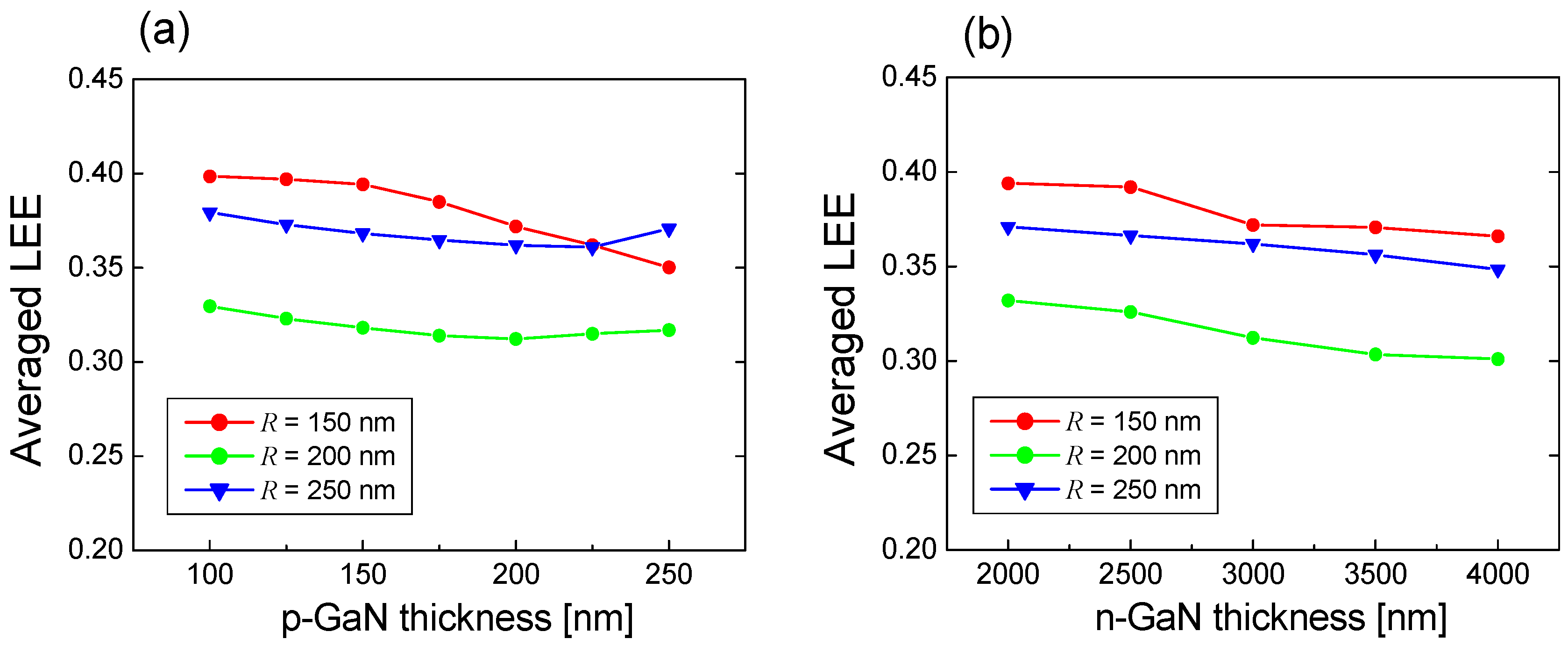
In order to find the optimum p-GaN and n-GaN thicknesses of the nanorod LED structures, the averaged LEE were calculated as the p-GaN or n-GaN thickness varies for the rod radius of 150, 200, and 250 nm, as shown in
Figure 5. As the p-GaN thickness increases, the averaged LEE of the rod radius 150 nm decreases, and that of the rod radii 200 and 250 nm initially decreases and begins to increase at the p-GaN thickness larger than 200 nm. This behavior could also be explained by the resonant mode analysis. However, the variation of the LEE with the p-GaN or n-GaN thickness is not so large when compared to the LEE variation with the rod radius in
Figure 4. The variation of the LEE with the p-GaN or n-GaN thickness is less than 5% for a given rod radius. It is not easy to explain this small difference by the resonant mode profiles, and the p-GaN or n-GaN thickness does not have a significant influence on resonant mode profiles inside the nanorod as compared to the influence of the rod radius on the resonant mode profiles. Nevertheless, the optimum thicknesses for achieving the highest LEE are 100 to 150 nm for the p-GaN thickness and 2000 to 2500 nm for the n-GaN thickness when the rod radius is 150 nm.
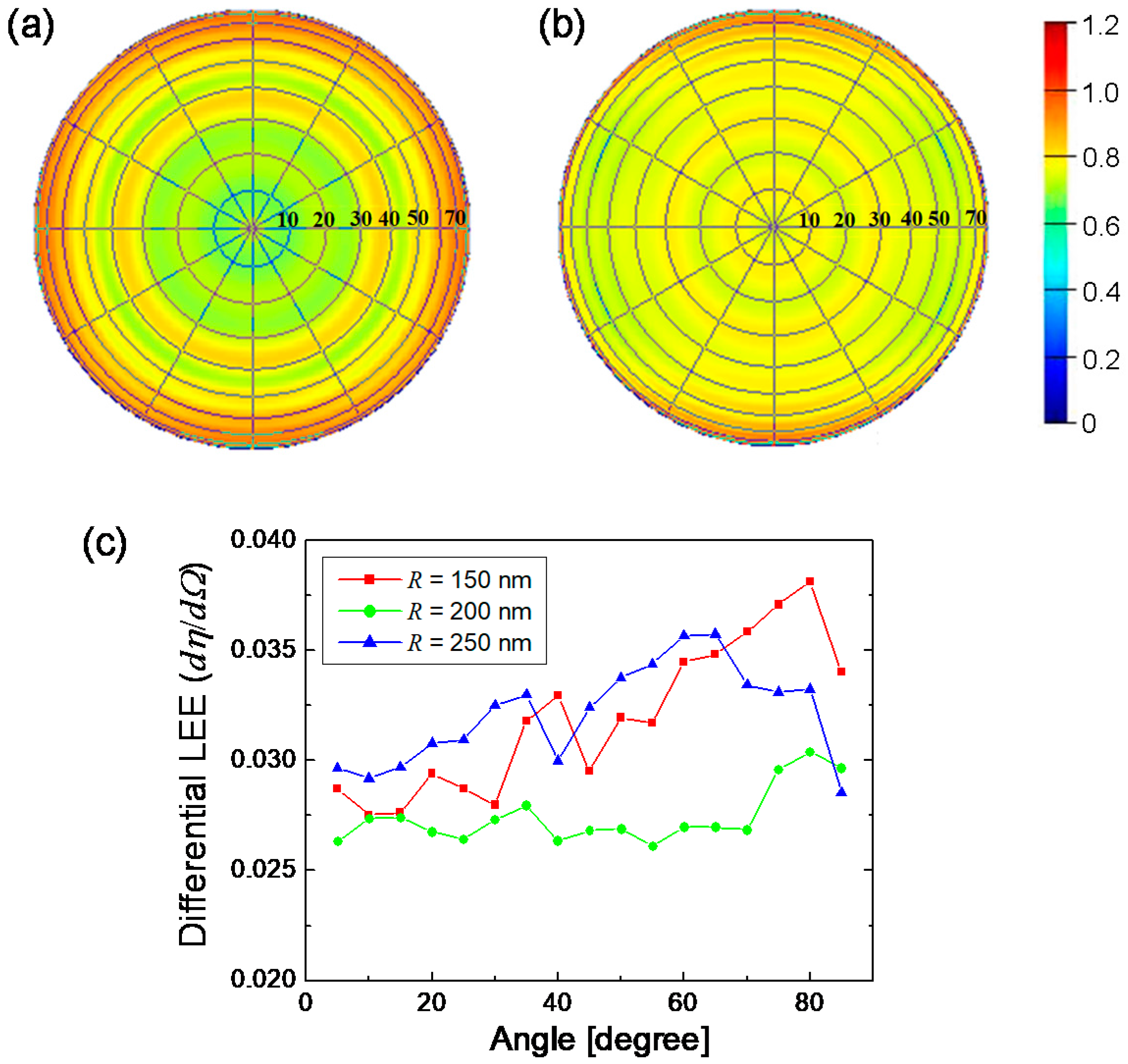
Finally, the angular distribution of the far-field pattern (FFP) is calculated.
Figure 6a,b show the two-dimensional polar plot of the electric field intensity of FFP on the upper hemisphere for the nanorod radius of 150 and 200 nm, respectively. The angular distribution was averaged over source position and polarization direction, according to Equation (3). It was also spectrally averaged, according to Equation (1). Circularly symmetric distribution is observed as expected. For the rod radius of 150 nm, FFP becomes stronger as the polar angle increases, implying that the emission in the horizontal direction (
x-
y direction in
Figure 1) is relatively strong. For the rod radius of 200 nm, reasonably uniform emission is observed excep for a large polar angle >70°.
Figure 6c shows the one-dimensional angluar distribution of the averaged LEE. It is the differential LEE as a function of the polar angle.
The differential LEE is calculated as
where
is the interval of the polar angle that is set to be 5° here. The angular dependence of the differential LEE also exhibits similar behavior to the FFP distribution. For the rod radius of 150 nm, the differential LEE mostly increases with polar angle, resulting in high differential LEE values at large polar angle. For the rod radius of 200 nm, quite uniform differential LEE is observed up to 70°. In this case, Lambertian-like distribution of emission from the nanorod LED can be obtained, although the LEE of this rod radius is somewhat lower than that of other rod radii. The result implies that the emission distribution from the nanorod LED can be tailored by optimizing the nanorod structural parameters.
