
Advanced Scanning Probe Microscopy of Graphene and Other 2D Materials


Abstract
:1. Introduction
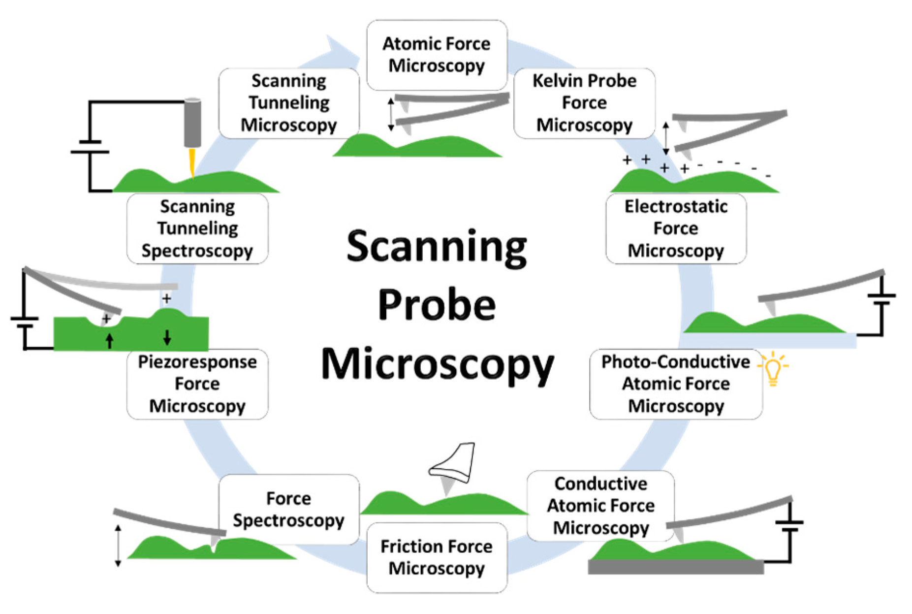
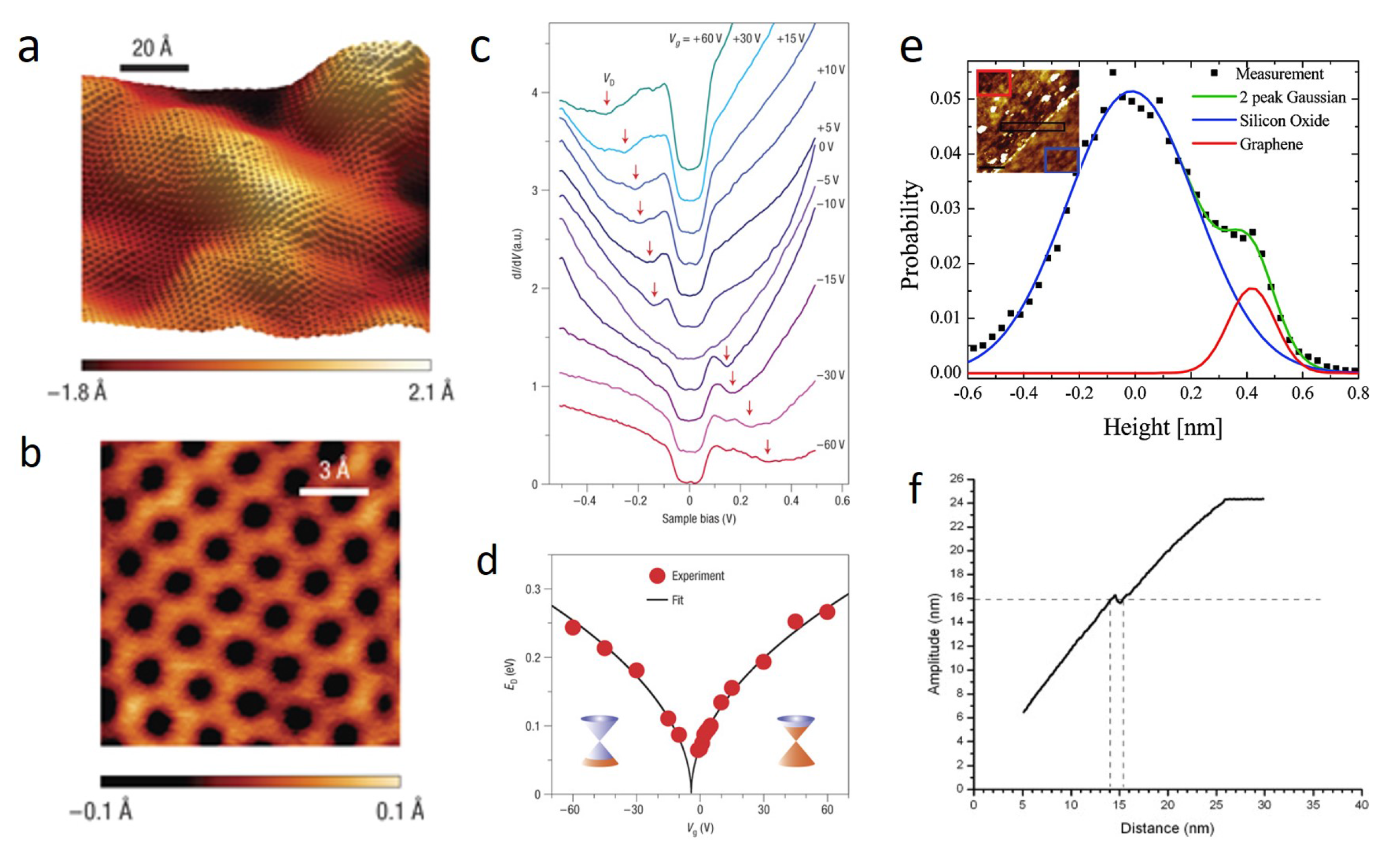
2. Scanning Tunneling Microscopy
3. Atomic Force Microscopy
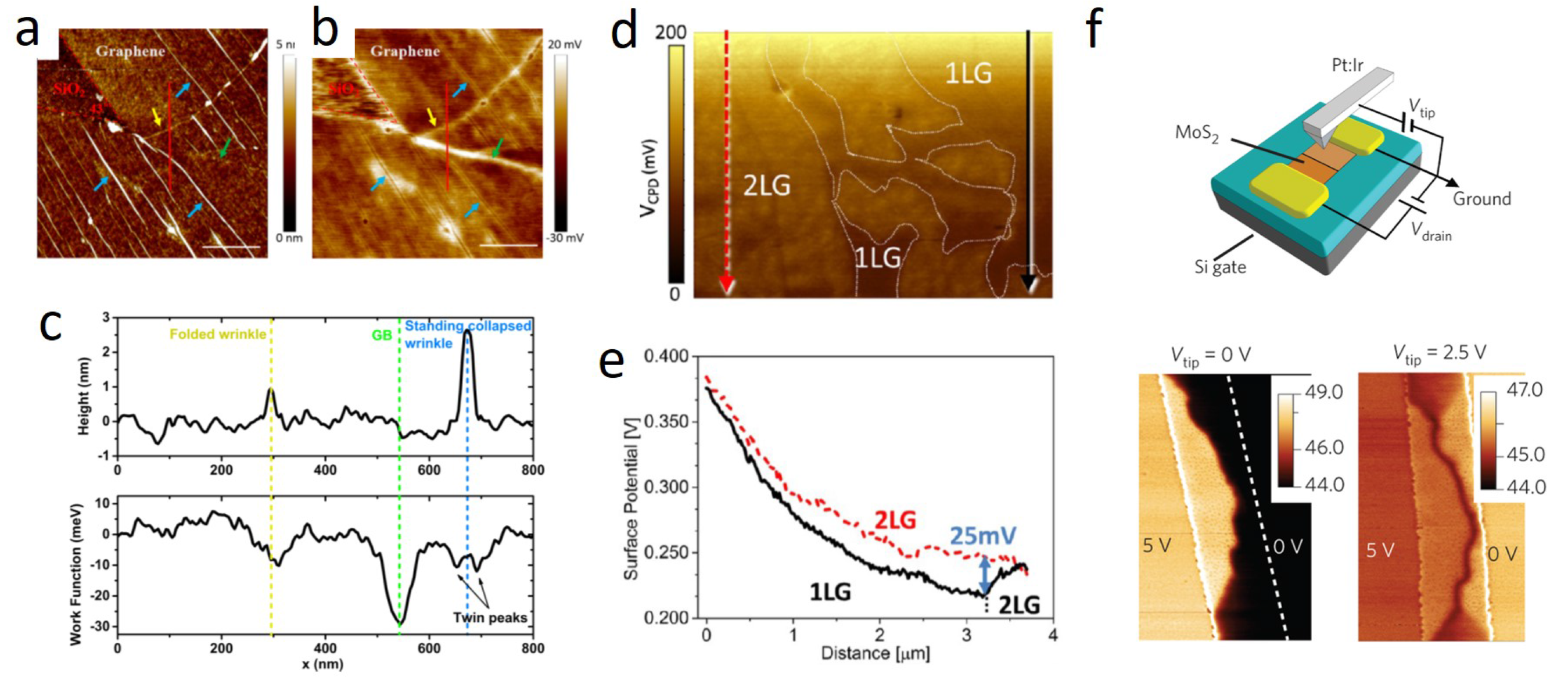
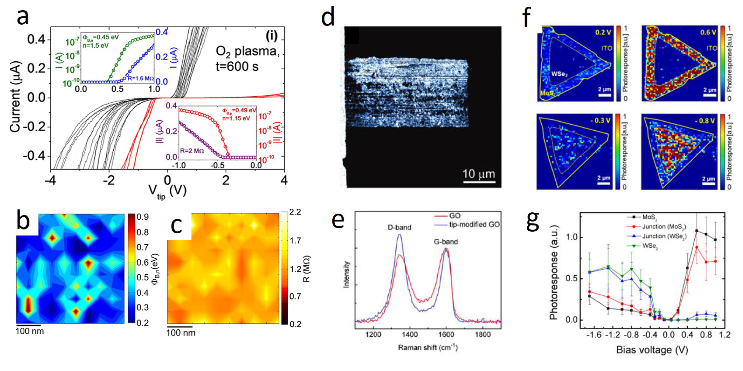
4. Electrical Modes
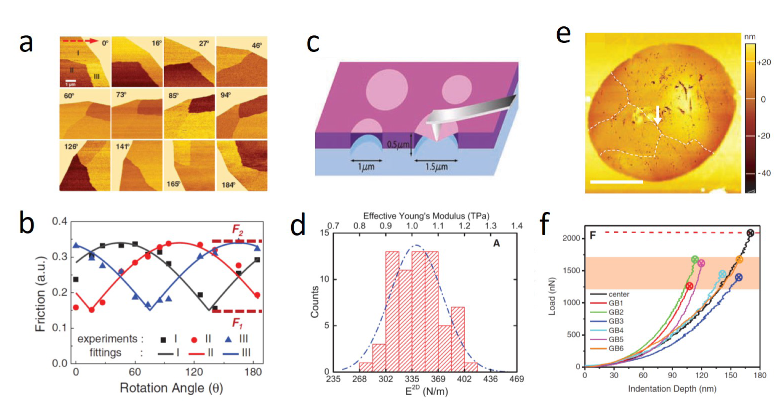
5. Friction Force Microscopy
6. Force Spectroscopy
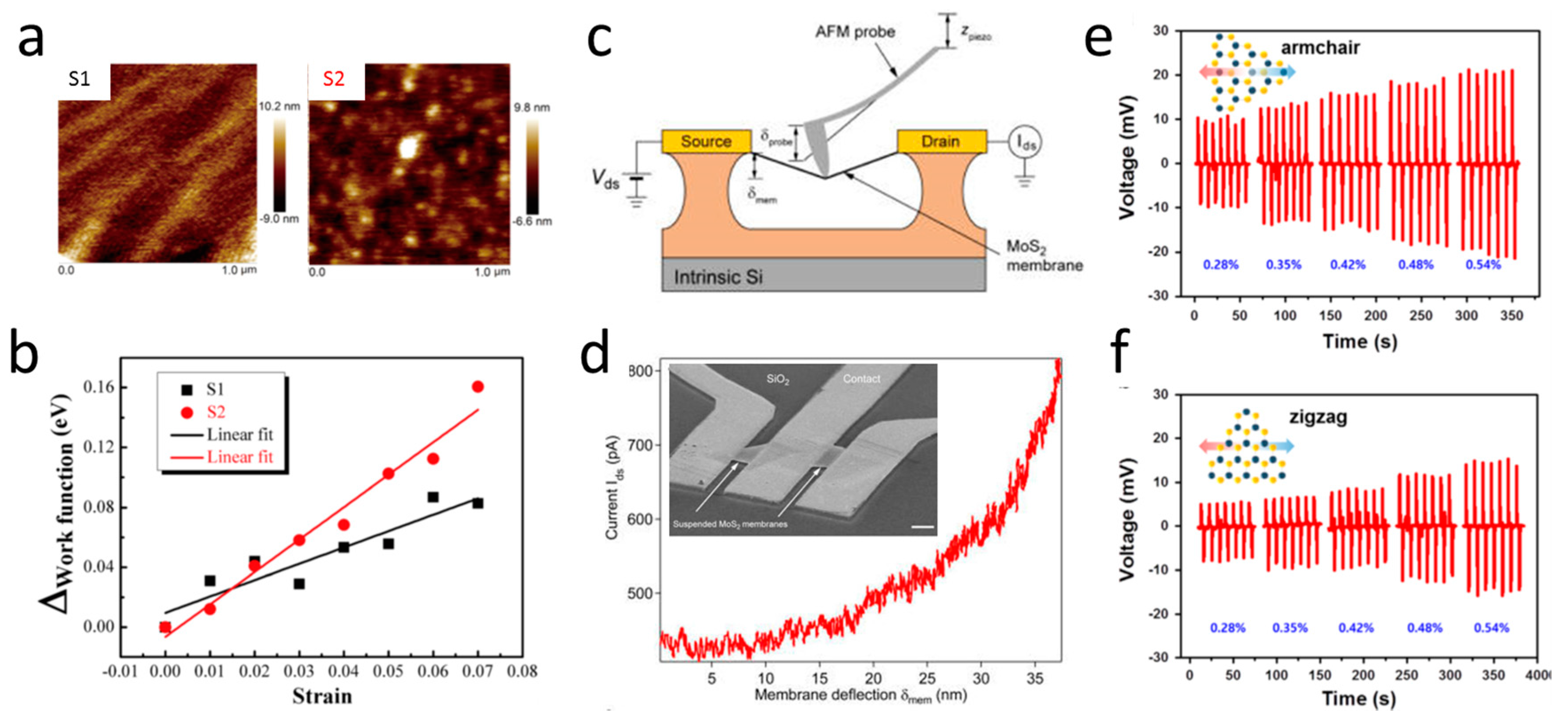
7. Strain Engineering and Piezoresponse Force Microscopy
8. Conclusions
Conflicts of Interest
References
- Schwierz, F. Graphene transistors. Nat. Nanotechnol. 2010, 5, 487–496. [Google Scholar] [CrossRef] [PubMed]
- Jariwala, D.; Sangwan, V.K.; Lauhon, L.J.; Marks, T.J.; Hersam, M.C. Emerging device applications for semiconducting two-dimensional transition metal dichalcogenides. ACS Nano 2014, 8, 1102–1120. [Google Scholar] [CrossRef] [PubMed]
- Cain, J.D.; Hanson, E.D.; Shi, F.; Dravid, V.P. Emerging opportunities in the two-dimensional chalcogenide systems and architecture. Curr. Opin. Solid State Mater. Sci. 2016, 20, 374–387. [Google Scholar] [CrossRef]
- Allen, M.J.; Tung, V.C.; Kaner, R.B. Honeycomb carbon: A review of graphene. Chem. Rev. 2010, 110, 132–145. [Google Scholar] [CrossRef] [PubMed]
- Novoselov, K.S.; Geim, A.K.; Morozov, S.V.; Jiang, D.; Katsnelson, M.I.; Grigorieva, I.V.; Dubonos, S.V.; Firsov, A.A. Two-dimensional gas of massless dirac fermions in graphene. Nature 2005, 438, 197–200. [Google Scholar] [CrossRef] [PubMed]
- Zhang, Y.; Tan, Y.-W.; Stormer, H.L.; Kim, P. Experimental observation of the quantum hall effect and berry's phase in graphene. Nature 2005, 438, 201–204. [Google Scholar] [CrossRef] [PubMed]
- Geim, A.K.; Novoselov, K.S. The rise of graphene. Nat. Mater. 2007, 6, 183–191. [Google Scholar] [CrossRef] [PubMed]
- Castro Neto, A.H.; Guinea, F.; Peres, N.M.R.; Novoselov, K.S.; Geim, A.K. The electronic properties of graphene. Rev. Mod. Phys. 2009, 81, 109–162. [Google Scholar] [CrossRef]
- Geim, A.K. Graphene: Status and prospects. Science 2009, 324, 1530–1534. [Google Scholar] [CrossRef] [PubMed]
- Butler, S.Z.; Hollen, S.M.; Cao, L.; Cui, Y.; Gupta, J.A.; Gutiérrez, H.R.; Heinz, T.F.; Hong, S.S.; Huang, J.; Ismach, A.F.; et al. Progress, challenges, and opportunities in two-dimensional materials beyond graphene. ACS Nano 2013, 7, 2898–2926. [Google Scholar] [CrossRef] [PubMed]
- Geim, A.K.; Grigorieva, I.V. Van der Waals heterostructures. Nature 2013, 499, 419–425. [Google Scholar] [CrossRef] [PubMed]
- Wang, F.; Wang, Z.; Xu, K.; Wang, F.; Wang, Q.; Huang, Y.; Yin, L.; He, J. Tunable gate-MoS2 Van der Waals p–n junctions with novel optoelectronic performance. Nano Lett. 2015, 15, 7558–7566. [Google Scholar] [CrossRef] [PubMed]
- Radisavljevic, B.; Radenovic, A.; Brivio, J.; Giacometti, V.; Kis, A. Single-layer MoS2 transistors. Nat. Nanotechnol. 2011, 6, 147–150. [Google Scholar] [CrossRef] [PubMed]
- Wang, H.; Yu, L.; Lee, Y.-H.; Shi, Y.; Hsu, A.; Chin, M.L.; Li, L.-J.; Dubey, M.; Kong, J.; Palacios, T. Integrated circuits based on bilayer MoS2 transistors. Nano Lett. 2012, 12, 4674–4680. [Google Scholar] [CrossRef] [PubMed]
- Krasnozhon, D.; Lembke, D.; Nyffeler, C.; Leblebici, Y.; Kis, A. MoS2 transistors operating at gigahertz frequencies. Nano Lett. 2014, 14, 5905–5911. [Google Scholar] [CrossRef] [PubMed]
- Lee, S.; Sohn, J.; Jiang, Z.; Chen, H.-Y.; Philip Wong, H.S. Metal oxide-resistive memory using graphene-edge electrodes. Nat. Commun. 2015, 6, 8407. [Google Scholar] [CrossRef] [PubMed]
- Han, S.-T.; Zhou, Y.; Chen, B.; Wang, C.; Zhou, L.; Yan, Y.; Zhuang, J.; Sun, Q.; Zhang, H.; Roy, V.A.L. Hybrid flexible resistive random access memory-gated transistor for novel nonvolatile data storage. Small 2016, 12, 390–396. [Google Scholar] [CrossRef] [PubMed]
- Sangwan, V.K.; Jariwala, D.; Kim, I.S.; Chen, K.-S.; Marks, T.J.; Lauhon, L.J.; Hersam, M.C. Gate-tunable memristive phenomena mediated by grain boundaries in single-layer MoS2. Nat. Nano 2015, 10, 403–406. [Google Scholar] [CrossRef] [PubMed]
- Musumeci, C.; Liscio, A.; Palermo, V.; Samorì, P. Electronic characterization of supramolecular materials at the nanoscale by conductive atomic force and kelvin probe force microscopies. Mater. Today 2014, 17, 504. [Google Scholar] [CrossRef]
- Liscio, A.; Palermo, V.; Samorì, P. Nanoscale quantitative measurement of the potential of charged nanostructures by electrostatic and kelvin probe force microscopy: Unraveling electronic processes in complex materials. Acc. Chem. Res. 2010, 43, 541–550. [Google Scholar] [CrossRef] [PubMed]
- Deshpande, A.; LeRoy, B.J. Scanning probe microscopy of graphene. Phys. E 2012, 44, 743–759. [Google Scholar] [CrossRef]
- Meyer, J.C.; Geim, A.K.; Katsnelson, M.I.; Novoselov, K.S.; Booth, T.J.; Roth, S. The structure of suspended graphene sheets. Nature 2007, 446, 60–63. [Google Scholar] [CrossRef] [PubMed]
- Fasolino, A.; Los, J.H.; Katsnelson, M.I. Intrinsic ripples in graphene. Nat. Mater. 2007, 6, 858–861. [Google Scholar] [CrossRef] [PubMed]
- Miao, F.; Wijeratne, S.; Zhang, Y.; Coskun, U.C.; Bao, W.; Lau, C.N. Phase-coherent transport in graphene quantum billiards. Science 2007, 317, 1530–1533. [Google Scholar] [CrossRef] [PubMed]
- Yazyev, O.V.; Chen, Y.P. Polycrystalline graphene and other two-dimensional materials. Nat. Nano 2014, 9, 755–767. [Google Scholar] [CrossRef] [PubMed]
- Zhang, Z.; Zou, X.; Crespi, V.H.; Yakobson, B.I. Intrinsic magnetism of grain boundaries in two-dimensional metal dichalcogenides. ACS Nano 2013, 7, 10475–10481. [Google Scholar] [CrossRef] [PubMed]
- Zou, X.; Yakobson, B.I. An open canvas—2D materials with defects, disorder, and functionality. Acc. Chem. Res. 2015, 48, 73–80. [Google Scholar] [CrossRef] [PubMed]
- Rafael, R.; Andrés, C.-G.; Emmanuele, C.; Francisco, G. Strain engineering in semiconducting two-dimensional crystals. J. Phys. Condens. Matter 2015, 27, 313201. [Google Scholar]
- Binnig, G.; Rohrer, H.; Gerber, C.; Weibel, E. Surface studies by scanning tunneling microscopy. Phys. Rev. Lett. 1982, 49, 57–61. [Google Scholar] [CrossRef]
- Zhang, R.; Ivey, D.G. Preparation of sharp polycrystalline tungsten tips for scanning tunneling microscopy imaging. J. Vac. Sci. Technol. B 1996, 14, 1–10. [Google Scholar] [CrossRef]
- Khan, Y.; Al-Falih, H.; Zhang, Y.; Ng, T.K.; Ooi, B.S. Two-step controllable electrochemical etching of tungsten scanning probe microscopy tips. Rev. Sci. Instrum. 2012, 83, 063708. [Google Scholar] [CrossRef] [PubMed]
- Yamada, T.K.; Abe, T.; Nazriq, N.M.K.; Irisawa, T. Electron-bombarded <110>-oriented tungsten tips for stable tunneling electron emission. Rev. Sci. Instrum. 2016, 87, 033703. [Google Scholar] [CrossRef] [PubMed]
- Stolyarova, E.; Rim, K.T.; Ryu, S.; Maultzsch, J.; Kim, P.; Brus, L.E.; Heinz, T.F.; Hybertsen, M.S.; Flynn, G.W. High-resolution scanning tunneling microscopy imaging of mesoscopic graphene sheets on an insulating surface. Proc. Natl. Acad. Sci. USA 2007, 104, 9209–9212. [Google Scholar] [CrossRef] [PubMed]
- Zhang, Y.; Brar, V.W.; Wang, F.; Girit, C.; Yayon, Y.; Panlasigui, M.; Zettl, A.; Crommie, M.F. Giant phonon-induced conductance in scanning tunnelling spectroscopy of gate-tunable graphene. Nat. Phys. 2008, 4, 627–630. [Google Scholar] [CrossRef]
- Ishigami, M.; Chen, J.H.; Cullen, W.G.; Fuhrer, M.S.; Williams, E.D. Atomic structure of graphene on SiO2. Nano Lett. 2007, 7, 1643–1648. [Google Scholar] [CrossRef] [PubMed]
- Berger, C.; Song, Z.; Li, X.; Wu, X.; Brown, N.; Naud, C.; Mayou, D.; Li, T.; Hass, J.; Marchenkov, A.N.; et al. Electronic confinement and coherence in patterned epitaxial graphene. Science 2006, 312, 1191–1196. [Google Scholar] [CrossRef] [PubMed]
- Moran-Meza, J.A.; Cousty, J.; Lubin, C.; Thoyer, F. Understanding the STM images of epitaxial graphene on a reconstructed 6H-SiC(0001) surface: The role of tip-induced mechanical distortion of graphene. Phys. Chem. Chem. Phys. 2016, 18, 14264–14272. [Google Scholar] [CrossRef] [PubMed]
- Coraux, J.; N’Diaye, A.T.; Busse, C.; Michely, T. Structural coherency of graphene on Ir(111). Nano Lett. 2008, 8, 565–570. [Google Scholar] [CrossRef] [PubMed]
- Kwon, S.-Y.; Ciobanu, C.V.; Petrova, V.; Shenoy, V.B.; Bareño, J.; Gambin, V.; Petrov, I.; Kodambaka, S. Growth of semiconducting graphene on palladium. Nano Lett. 2009, 9, 3985–3990. [Google Scholar] [CrossRef] [PubMed]
- Gao, L.; Guest, J.R.; Guisinger, N.P. Epitaxial graphene on Cu(111). Nano Lett. 2010, 10, 3512–3516. [Google Scholar] [CrossRef] [PubMed]
- Dubout, Q.; Calleja, F.; Sclauzero, G.; Etzkorn, M.; Lehnert, A.; Claude, L.; Papagno, M.; Natterer, F.D.; Patthey, F.; Rusponi, S.; et al. Giant apparent lattice distortions in STM images of corrugated sp2-hybridised monolayers. New J. Phys. 2016, 18, 103027. [Google Scholar] [CrossRef]
- Xue, J.; Sanchez-Yamagishi, J.; Bulmash, D.; Jacquod, P.; Deshpande, A.; Watanabe, K.; Taniguchi, T.; Jarillo-Herrero, P.; LeRoy, B.J. Scanning tunnelling microscopy and spectroscopy of ultra-flat graphene on hexagonal boron nitride. Nat. Mater. 2011, 10, 282–285. [Google Scholar] [CrossRef] [PubMed]
- Harners, R.J. Atomic-resolution surface spectroscopy with the scanning tunneling microscope. Annu. Rev. Phys. Chem. 1989, 40, 531–559. [Google Scholar]
- Tromp, R.M. Spectroscopy with the scanning tunnelling microscope: A critical review. J. Phys. Condens. Matter 1989, 1, 10211. [Google Scholar] [CrossRef]
- Liu, H.; Zheng, H.; Yang, F.; Jiao, L.; Chen, J.; Ho, W.; Gao, C.; Jia, J.; Xie, M. Line and point defects in MoSe2 bilayer studied by scanning tunneling microscopy and spectroscopy. ACS Nano 2015, 9, 6619–6625. [Google Scholar] [CrossRef] [PubMed]
- Park, J.H.; Vishwanath, S.; Liu, X.; Zhou, H.; Eichfeld, S.M.; Fullerton-Shirey, S.K.; Robinson, J.A.; Feenstra, R.M.; Furdyna, J.; Jena, D.; et al. Scanning tunneling microscopy and spectroscopy of air exposure effects on molecular beam epitaxy grown WSe2 monolayers and bilayers. ACS Nano 2016, 10, 4258–4267. [Google Scholar] [CrossRef] [PubMed]
- Huang, Y.L.; Chen, Y.; Zhang, W.; Quek, S.Y.; Chen, C.-H.; Li, L.-J.; Hsu, W.-T.; Chang, W.-H.; Zheng, Y.J.; Chen, W.; et al. Bandgap tunability at single-layer molybdenum disulphide grain boundaries. Nat. Commun. 2015, 6, 6298. [Google Scholar] [CrossRef] [PubMed]
- Georgi, A.; Nemes-Incze, P.; Carrillo-Bastos, R.; Faria, D.; Viola Kusminskiy, S.; Zhai, D.; Schneider, M.; Subramaniam, D.; Mashoff, T.; Freitag, N.M.; et al. Tuning the pseudospin polarization of graphene by a pseudomagnetic field. Nano Lett. 2017, 17, 2240–2245. [Google Scholar] [CrossRef] [PubMed]
- Philippe, D.; Viet Hung, N.; Jérôme, S.-M. Thermoelectric effects in graphene nanostructures. J. Phys. Condens. Matter 2015, 27, 133204. [Google Scholar]
- Park, J.; He, G.; Feenstra, R.M.; Li, A.-P. Atomic-scale mapping of thermoelectric power on graphene: Role of defects and boundaries. Nano Lett. 2013, 13, 3269–3273. [Google Scholar] [CrossRef] [PubMed]
- Nemes-Incze, P.; Osváth, Z.; Kamarás, K.; Biró, L.P. Anomalies in thickness measurements of graphene and few layer graphite crystals by tapping mode atomic force microscopy. Carbon 2008, 46, 1435–1442. [Google Scholar] [CrossRef]
- Binnig, G.; Quate, C.F.; Gerber, C. Atomic force microscope. Phys. Rev. Lett. 1986, 56, 930–933. [Google Scholar] [CrossRef] [PubMed]
- Wang, Y.; Yang, R.; Shi, Z.; Zhang, L.; Shi, D.; Wang, E.; Zhang, G. Super-elastic graphene ripples for flexible strain sensors. ACS Nano 2011, 5, 3645–3650. [Google Scholar] [CrossRef] [PubMed]
- Burnett, T.L.; Yakimova, R.; Kazakova, O. Identification of epitaxial graphene domains and adsorbed species in ambient conditions using quantified topography measurements. J. Appl. Phys. 2012, 112, 054308. [Google Scholar] [CrossRef]
- Kim, J.-S.; Choi, J.S.; Lee, M.J.; Park, B.H.; Bukhvalov, D.; Son, Y.-W.; Yoon, D.; Cheong, H.; Yun, J.-N.; Jung, Y.; et al. Between Scylla and Charybdis: Hydrophobic graphene-guided water diffusion on hydrophilic substrates. Sci. Rep. 2013, 3, 2309. [Google Scholar] [CrossRef] [PubMed]
- Novoselov, K.S.; Jiang, D.; Schedin, F.; Booth, T.J.; Khotkevich, V.V.; Morozov, S.V.; Geim, A.K. Two-dimensional atomic crystals. Proc. Natl. Acad. Sci. USA 2005, 102, 10451–10453. [Google Scholar] [CrossRef] [PubMed]
- Russo, P.; Compagnini, G.; Musumeci, C.; Pignataro, B. Raman monitoring of strain induced effects in mechanically deposited single layer graphene. J. Nanosci. Nanotechnol. 2012, 12, 8755–8758. [Google Scholar] [CrossRef] [PubMed]
- Robinson, B.J.; Giusca, C.E.; Gonzalez, Y.T.; Kay, N.D.; Kazakova, O.; Kolosov, O.V. Structural, optical and electrostatic properties of single and few-layers MoS2: Effect of substrate. 2D Mater. 2015, 2, 015005. [Google Scholar] [CrossRef]
- Lee, Y.-H.; Zhang, X.-Q.; Zhang, W.; Chang, M.-T.; Lin, C.-T.; Chang, K.-D.; Yu, Y.-C.; Wang, J.T.-W.; Chang, C.-S.; Li, L.-J.; et al. Synthesis of large-area MoS2 atomic layers with chemical vapor deposition. Adv. Mater. 2012, 24, 2320–2325. [Google Scholar] [CrossRef] [PubMed]
- Mechler, Á.; Kopniczky, J.; Kokavecz, J.; Hoel, A.; Granqvist, C.-G.; Heszler, P. Anomalies in nanostructure size measurements by AFM. Phys. Rev. B 2005, 72, 125407. [Google Scholar] [CrossRef]
- García, R.; San Paulo, A. Attractive and repulsive tip-sample interaction regimes in tapping-mode atomic force microscopy. Phys. Rev. B 1999, 60, 4961–4967. [Google Scholar] [CrossRef]
- Cameron, J.S.; Ashley, D.S.; Andrew, J.S.; Joseph, G.S.; Christopher, T.G. Accurate thickness measurement of graphene. Nanotechnology 2016, 27, 125704. [Google Scholar]
- Ly, T.H.; Chiu, M.-H.; Li, M.-Y.; Zhao, J.; Perello, D.J.; Cichocka, M.O.; Oh, H.M.; Chae, S.H.; Jeong, H.Y.; Yao, F.; et al. Observing grain boundaries in CVD-grown monolayer transition metal dichalcogenides. ACS Nano 2014, 8, 11401–11408. [Google Scholar] [CrossRef] [PubMed]
- Duong, D.L.; Han, G.H.; Lee, S.M.; Gunes, F.; Kim, E.S.; Kim, S.T.; Kim, H.; Ta, Q.H.; So, K.P.; Yoon, S.J.; et al. Probing graphene grain boundaries with optical microscopy. Nature 2012, 490, 235–239. [Google Scholar] [CrossRef] [PubMed]
- Leng, Y.; Williams, C.C. Molecular Charge Mapping with Electrostatic Force Microscope; SPIE: Bellingham, WA, USA, 1993; pp. 35–39. [Google Scholar]
- Nonnenmacher, M.; O’Boyle, M.P.; Wickramasinghe, H.K. Kelvin probe force microscopy. Appl. Phys. Lett. 1991, 58, 2921–2923. [Google Scholar] [CrossRef]
- O’Shea, S.J.; Atta, R.M.; Murrell, M.P.; Welland, M.E. Conducting atomic force microscopy study of silicon dioxide breakdown. J. Vac. Sci. Technol. B 1995, 13, 1945–1952. [Google Scholar] [CrossRef]
- Avila, A.; Bhushan, B. Electrical measurement techniques in atomic force microscopy. Crit. Rev. Solid State Mater. Sci. 2010, 35, 38–51. [Google Scholar] [CrossRef]
- Coffey, D.C.; Reid, O.G.; Rodovsky, D.B.; Bartholomew, G.P.; Ginger, D.S. Mapping local photocurrents in polymer/fullerene solar cells with photoconductive atomic force microscopy. Nano Lett. 2007, 7, 738–744. [Google Scholar] [CrossRef] [PubMed]
- Jacobs, H.O.; Leuchtmann, P.; Homan, O.J.; Stemmer, A. Resolution and contrast in kelvin probe force microscopy. J. Appl. Phys. 1998, 84, 1168–1173. [Google Scholar] [CrossRef]
- Hormeno, S.; Penedo, M.; Manzano, C.V.; Luna, M. Gold nanoparticle coated silicon tips for kelvin probe force microscopy in air. Nanotechnology 2013, 24, 395701. [Google Scholar] [CrossRef] [PubMed]
- Lanza, M.; Bayerl, A.; Gao, T.; Porti, M.; Nafria, M.; Jing, G.Y.; Zhang, Y.F.; Liu, Z.F.; Duan, H.L. Graphene-coated atomic force microscope tips for reliable nanoscale electrical characterization. Adv. Mater. 2013, 25, 1440–1444. [Google Scholar] [CrossRef] [PubMed]
- Hui, F.; Vajha, P.; Shi, Y.; Ji, Y.; Duan, H.; Padovani, A.; Larcher, L.; Li, X.R.; Xu, J.J.; Lanza, M. Moving graphene devices from lab to market: Advanced graphene-coated nanoprobes. Nanoscale 2016, 8, 8466–8473. [Google Scholar] [CrossRef] [PubMed]
- Kazakova, O.; Panchal, V.; Burnett, T. Epitaxial graphene and graphene-based devices studied by electrical scanning probe microscopy. Crystals 2013, 3, 191. [Google Scholar] [CrossRef]
- Burnett, T.; Yakimova, R.; Kazakova, O. Mapping of local electrical properties in epitaxial graphene using electrostatic force microscopy. Nano Lett. 2011, 11, 2324–2328. [Google Scholar] [CrossRef] [PubMed]
- Panchal, V.; Pearce, R.; Yakimova, R.; Tzalenchuk, A.; Kazakova, O. Standardization of surface potential measurements of graphene domains. Sci. Rep. 2013, 3, 2597. [Google Scholar] [CrossRef] [PubMed]
- Ziegler, D.; Gava, P.; Güttinger, J.; Molitor, F.; Wirtz, L.; Lazzeri, M.; Saitta, A.M.; Stemmer, A.; Mauri, F.; Stampfer, C. Variations in the work function of doped single- and few-layer graphene assessed by kelvin probe force microscopy and density functional theory. Phys. Rev. B 2011, 83, 235434. [Google Scholar] [CrossRef]
- Eriksson, J.; Pearce, R.; Iakimov, T.; Virojanadara, C.; Gogova, D.; Andersson, M.; Syväjärvi, M.; Lloyd Spetz, A.; Yakimova, R. The influence of substrate morphology on thickness uniformity and unintentional doping of epitaxial graphene on SiC. Appl. Phys. Lett. 2012, 100, 241607. [Google Scholar] [CrossRef]
- Long, F.; Yasaei, P.; Sanoj, R.; Yao, W.; Král, P.; Salehi-Khojin, A.; Shahbazian-Yassar, R. Characteristic work function variations of graphene line defects. ACS Appl. Mater. Interfaces 2016, 8, 18360–18366. [Google Scholar] [CrossRef] [PubMed]
- Pearce, R.; Eriksson, J.; Iakimov, T.; Hultman, L.; Lloyd Spetz, A.; Yakimova, R. On the differing sensitivity to chemical gating of single and double layer epitaxial graphene explored using scanning kelvin probe microscopy. ACS Nano 2013, 7, 4647–4656. [Google Scholar] [CrossRef] [PubMed]
- Kulkarni, D.D.; Kim, S.; Chyasnavichyus, M.; Hu, K.; Fedorov, A.G.; Tsukruk, V.V. Chemical reduction of individual graphene oxide sheets as revealed by electrostatic force microscopy. J. Am. Chem. Soc. 2014, 136, 6546–6549. [Google Scholar] [CrossRef] [PubMed]
- Yu, Y.-J.; Zhao, Y.; Ryu, S.; Brus, L.E.; Kim, K.S.; Kim, P. Tuning the graphene work function by electric field effect. Nano Lett. 2009, 9, 3430–3434. [Google Scholar] [CrossRef] [PubMed]
- Fisichella, G.; Greco, G.; Roccaforte, F.; Giannazzo, F. Current transport in graphene/AlGaN/GaN vertical heterostructures probed at nanoscale. Nanoscale 2014, 6, 8671–8680. [Google Scholar] [CrossRef] [PubMed]
- Fisichella, G.; Di Franco, S.; Fiorenza, P.; Lo Nigro, R.; Roccaforte, F.; Tudisco, C.; Condorelli, G.G.; Piluso, N.; Spartà, N.; Lo Verso, S.; et al. Micro- and nanoscale electrical characterization of large-area graphene transferred to functional substrates. Beilstein J. Nanotechnol. 2013, 4, 234–242. [Google Scholar] [CrossRef] [PubMed]
- Kellar, J.A.; Alaboson, J.M.P.; Wang, Q.H.; Hersam, M.C. Identifying and characterizing epitaxial graphene domains on partially graphitized SiC(0001) surfaces using scanning probe microscopy. Appl. Phys. Lett. 2010, 96, 143103. [Google Scholar] [CrossRef]
- Giannazzo, F.; Deretzis, I.; La Magna, A.; Roccaforte, F.; Yakimova, R. Electronic transport at monolayer-bilayer junctions in epitaxial graphene on SiC. Phys. Rev. B 2012, 86, 235422. [Google Scholar] [CrossRef]
- Sonde, S.; Giannazzo, F.; Raineri, V.; Yakimova, R.; Huntzinger, J.R.; Tiberj, A.; Camassel, J. Electrical properties of the graphene/4H-SiC(0001) interface probed by scanning current spectroscopy. Phys. Rev. B 2009, 80. [Google Scholar] [CrossRef]
- Giannazzo, F.; Fisichella, G.; Piazza, A.; Agnello, S.; Roccaforte, F. Nanoscale inhomogeneity of the Schottky barrier and resistivity in MoS2 multilayers. Phys. Rev. B 2015, 92. [Google Scholar] [CrossRef]
- Bampoulis, P.; van Bremen, R.; Yao, Q.; Poelsema, B.; Zandvliet, H.J.W.; Sotthewes, K. Defect dominated charge transport and fermi level pinning in MoS2/metal contacts. ACS Appl. Mater. Interfaces 2017, 9, 19278–19286. [Google Scholar] [CrossRef] [PubMed]
- Giannazzo, F.; Fisichella, G.; Greco, G.; Di Franco, S.; Deretzis, I.; La Magna, A.; Bongiorno, C.; Nicotra, G.; Spinella, C.; Scopelliti, M.; et al. Ambipolar MoS2 transistors by nanoscale tailoring of Schottky barrier using oxygen plasma functionalization. ACS Appl. Mater. Interfaces 2017. [Google Scholar] [CrossRef] [PubMed]
- Liu, H.; Hoeppener, S.; Schubert, U.S. Nanoscale materials patterning by local electrochemical lithography. Adv. Eng. Mater. 2016, 18, 890–902. [Google Scholar]
- Mativetsky, J.M.; Treossi, E.; Orgiu, E.; Melucci, M.; Veronese, G.P.; Samorì, P.; Palermo, V. Local current mapping and patterning of reduced graphene oxide. J. Am. Chem. Soc. 2010, 132, 14130–14136. [Google Scholar] [CrossRef] [PubMed]
- Faucett, A.C.; Mativetsky, J.M. Nanoscale reduction of graphene oxide under ambient conditions. Carbon 2015, 95, 1069–1075. [Google Scholar] [CrossRef]
- Byun, I.-S.; Yoon, D.; Choi, J.S.; Hwang, I.; Lee, D.H.; Lee, M.J.; Kawai, T.; Son, Y.-W.; Jia, Q.; Cheong, H.; et al. Nanoscale lithography on monolayer graphene using hydrogenation and oxidation. ACS Nano 2011, 5, 6417–6424. [Google Scholar] [CrossRef] [PubMed]
- Mativetsky, J.M.; Liscio, A.; Treossi, E.; Orgiu, E.; Zanelli, A.; Samorì, P.; Palermo, V. Graphene transistors via in situ voltage-induced reduction of graphene-oxide under ambient conditions. J. Am. Chem. Soc. 2011, 133, 14320–14326. [Google Scholar] [CrossRef] [PubMed]
- Son, Y.; Li, M.-Y.; Cheng, C.-C.; Wei, K.-H.; Liu, P.; Wang, Q.H.; Li, L.-J.; Strano, M.S. Observation of switchable photoresponse of a monolayer WSe2–MoS2 lateral heterostructure via photocurrent spectral atomic force microscopic imaging. Nano Lett. 2016, 16, 3571–3577. [Google Scholar] [CrossRef] [PubMed]
- Ruzmetov, D.; Zhang, K.; Stan, G.; Kalanyan, B.; Bhimanapati, G.R.; Eichfeld, S.M.; Burke, R.A.; Shah, P.B.; O’Regan, T.P.; Crowne, F.J.; et al. Vertical 2D/3D semiconductor heterostructures based on epitaxial molybdenum disulfide and gallium nitride. ACS Nano 2016, 10, 3580–3588. [Google Scholar] [CrossRef] [PubMed]
- Son, Y.; Wang, Q.H.; Paulson, J.A.; Shih, C.-J.; Rajan, A.G.; Tvrdy, K.; Kim, S.; Alfeeli, B.; Braatz, R.D.; Strano, M.S. Layer number dependence of MoS2 photoconductivity using photocurrent spectral atomic force microscopic imaging. ACS Nano 2015, 9, 2843–2855. [Google Scholar] [CrossRef] [PubMed]
- Mate, C.M.; McClelland, G.M.; Erlandsson, R.; Chiang, S. Atomic-scale friction of a tungsten tip on a graphite surface. Phys. Rev. Lett. 1987, 59, 1942–1945. [Google Scholar] [CrossRef] [PubMed]
- Bennewitz, R. Friction force microscopy. Mater. Today 2005, 8, 42–48. [Google Scholar] [CrossRef]
- Cain, R.G.; Biggs, S.; Page, N.W. Force calibration in lateral force microscopy. J. Colloid Interface Sci. 2000, 227, 55–65. [Google Scholar] [CrossRef] [PubMed]
- Gibson, C.T.; Watson, G.S.; Myhra, S. Lateral force microscopy—A quantitative approach. Wear 1997, 213, 72–79. [Google Scholar] [CrossRef]
- Marsden, A.J.; Phillips, M.; Wilson, N.R. Friction force microscopy: A simple technique for identifying graphene on rough substrates and mapping the orientation of graphene grains on copper. Nanotechnology 2013, 24, 255704. [Google Scholar] [CrossRef] [PubMed]
- Fujisawa, S.; Kishi, E.; Sugawara, Y.; Morita, S. Atomic-scale friction observed with a two-dimensional frictional-force microscope. Phys. Rev. B 1995, 51, 7849–7857. [Google Scholar] [CrossRef]
- Lee, C.; Li, Q.; Kalb, W.; Liu, X.-Z.; Berger, H.; Carpick, R.W.; Hone, J. Frictional characteristics of atomically thin sheets. Science 2010, 328, 76–80. [Google Scholar] [CrossRef] [PubMed]
- Choi, J.S.; Kim, J.-S.; Byun, I.-S.; Lee, D.H.; Lee, M.J.; Park, B.H.; Lee, C.; Yoon, D.; Cheong, H.; Lee, K.H.; et al. Friction anisotropy–driven domain imaging on exfoliated monolayer graphene. Science 2011, 333, 607–610. [Google Scholar] [CrossRef] [PubMed]
- Lee, C.; Wei, X.; Kysar, J.W.; Hone, J. Measurement of the elastic properties and intrinsic strength of monolayer graphene. Science 2008, 321, 385–388. [Google Scholar] [CrossRef] [PubMed]
- Lee, G.-H.; Cooper, R.C.; An, S.J.; Lee, S.; van der Zande, A.; Petrone, N.; Hammerberg, A.G.; Lee, C.; Crawford, B.; Oliver, W.; et al. High-strength chemical-vapor–deposited graphene and grain boundaries. Science 2013, 340, 1073–1076. [Google Scholar] [CrossRef] [PubMed]
- Butt, H.-J.; Cappella, B.; Kappl, M. Force measurements with the atomic force microscope: Technique, interpretation and applications. Surf. Sci. Rep. 2005, 59, 1–152. [Google Scholar] [CrossRef]
- Cappella, B.; Dietler, G. Force-distance curves by atomic force microscopy. Surf. Sci. Rep. 1999, 34, 1–104. [Google Scholar] [CrossRef]
- Liu, K.; Wu, J. Mechanical properties of two-dimensional materials and heterostructures. J. Mater. Res. 2016, 31, 832–844. [Google Scholar] [CrossRef]
- Hutter, J.L.; Bechhoefer, J. Calibration of atomic-force microscope tips. Rev. Sci. Instrum. 1993, 64, 1868–1873. [Google Scholar] [CrossRef]
- Poot, M.; van der Zant, H.S.J. Nanomechanical properties of few-layer graphene membranes. Appl. Phys. Lett. 2008, 92, 063111. [Google Scholar] [CrossRef]
- Palermo, V.; Kinloch, I.A.; Ligi, S.; Pugno, N.M. Nanoscale mechanics of graphene and graphene oxide in composites: A scientific and technological perspective. Adv. Mater. 2016, 28, 6232–6238. [Google Scholar] [CrossRef] [PubMed]
- Zandiatashbar, A.; Lee, G.-H.; An, S.J.; Lee, S.; Mathew, N.; Terrones, M.; Hayashi, T.; Picu, C.R.; Hone, J.; Koratkar, N. Effect of defects on the intrinsic strength and stiffness of graphene. Nat. Commun. 2014, 5, 3186. [Google Scholar] [CrossRef] [PubMed]
- Wei, X.; Mao, L.; Soler-Crespo, R.A.; Paci, J.T.; Huang, J.; Nguyen, S.T.; Espinosa, H.D. Plasticity and ductility in graphene oxide through a mechanochemically induced damage tolerance mechanism. Nat. Commun. 2015, 6, 8029. [Google Scholar] [CrossRef] [PubMed]
- Kunz, D.A.; Feicht, P.; Gödrich, S.; Thurn, H.; Papastavrou, G.; Fery, A.; Breu, J. Space-resolved in-plane moduli of graphene oxide and chemically derived graphene applying a simple wrinkling procedure. Adv. Mater. 2013, 25, 1337–1341. [Google Scholar] [CrossRef] [PubMed]
- Cao, C.; Daly, M.; Singh, C.V.; Sun, Y.; Filleter, T. High strength measurement of monolayer graphene oxide. Carbon 2015, 81, 497–504. [Google Scholar] [CrossRef]
- Suk, J.W.; Piner, R.D.; An, J.; Ruoff, R.S. Mechanical properties of monolayer graphene oxide. ACS Nano 2010, 4, 6557–6564. [Google Scholar] [CrossRef] [PubMed]
- Gómez-Navarro, C.; Burghard, M.; Kern, K. Elastic properties of chemically derived single graphene sheets. Nano Lett. 2008, 8, 2045–2049. [Google Scholar] [CrossRef] [PubMed]
- Lee, W.-K.; Kang, J.; Chen, K.-S.; Engel, C.J.; Jung, W.-B.; Rhee, D.; Hersam, M.C.; Odom, T.W. Multiscale, hierarchical patterning of graphene by conformal wrinkling. Nano Lett. 2016, 16, 7121–7127. [Google Scholar] [CrossRef] [PubMed]
- Castellanos-Gomez, A.; Poot, M.; Steele, G.A.; van der Zant, H.S.J.; Agraït, N.; Rubio-Bollinger, G. Elastic properties of freely suspended MoS2 nanosheets. Adv. Mater. 2012, 24, 772–775. [Google Scholar] [CrossRef] [PubMed]
- Song, L.; Ci, L.; Lu, H.; Sorokin, P.B.; Jin, C.; Ni, J.; Kvashnin, A.G.; Kvashnin, D.G.; Lou, J.; Yakobson, B.I.; et al. Large scale growth and characterization of atomic hexagonal boron nitride layers. Nano Lett. 2010, 10, 3209–3215. [Google Scholar] [CrossRef] [PubMed]
- Turchanin, A.; Beyer, A.; Nottbohm, C.T.; Zhang, X.; Stosch, R.; Sologubenko, A.; Mayer, J.; Hinze, P.; Weimann, T.; Gölzhäuser, A. One nanometer thin carbon nanosheets with tunable conductivity and stiffness. Adv. Mater. 2009, 21, 1233–1237. [Google Scholar] [CrossRef]
- Bertolazzi, S.; Brivio, J.; Kis, A. Stretching and breaking of ultrathin MoS2. ACS Nano 2011, 5, 9703–9709. [Google Scholar] [CrossRef] [PubMed]
- Klimov, N.N.; Jung, S.; Zhu, S.; Li, T.; Wright, C.A.; Solares, S.D.; Newell, D.B.; Zhitenev, N.B.; Stroscio, J.A. Electromechanical properties of graphene drumheads. Science 2012, 336, 1557–1561. [Google Scholar] [CrossRef] [PubMed]
- Xu, P.; Neek-Amal, M.; Barber, S.D.; Schoelz, J.K.; Ackerman, M.L.; Thibado, P.M.; Sadeghi, A.; Peeters, F.M. Unusual ultra-low-frequency fluctuations in freestanding graphene. Nat. Commun. 2014, 5, 3720. [Google Scholar] [CrossRef] [PubMed]
- Elibol, K.; Bayer, B.C.; Hummel, S.; Kotakoski, J.; Argentero, G.; Meyer, J.C. Visualising the strain distribution in suspended two-dimensional materials under local deformation. Sci. Rep. 2016, 6, 28485. [Google Scholar] [CrossRef] [PubMed]
- He, X.; Tang, N.; Sun, X.; Gan, L.; Ke, F.; Wang, T.; Xu, F.; Wang, X.; Yang, X.; Ge, W.; et al. Tuning the graphene work function by uniaxial strain. Appl. Phys. Lett. 2015, 106, 043106. [Google Scholar] [CrossRef]
- Manzeli, S.; Allain, A.; Ghadimi, A.; Kis, A. Piezoresistivity and strain-induced band gap tuning in atomically thin MoS2. Nano Lett. 2015, 15, 5330–5335. [Google Scholar] [CrossRef] [PubMed]
- Kim, S.K.; Bhatia, R.; Kim, T.-H.; Seol, D.; Kim, J.H.; Kim, H.; Seung, W.; Kim, Y.; Lee, Y.H.; Kim, S.-W. Directional dependent piezoelectric effect in cvd grown monolayer MoS2 for flexible piezoelectric nanogenerators. Nano Energy 2016, 22, 483–489. [Google Scholar] [CrossRef]
- Christman, J.A., Jr.; Woolcott, R.R., Jr.; Kingon, A.I.; Nemanich, R.J. Piezoelectric measurements with atomic force microscopy. Appl. Phys. Lett. 1998, 73, 3851–3853. [Google Scholar] [CrossRef]
- Güthner, P.; Dransfeld, K. Local poling of ferroelectric polymers by scanning force microscopy. Appl. Phys. Lett. 1992, 61, 1137–1139. [Google Scholar] [CrossRef]
- Kalinin, S.V.; Bonnell, D.A. Imaging mechanism of piezoresponse force microscopy of ferroelectric surfaces. Phys. Rev. B 2002, 65, 125408. [Google Scholar] [CrossRef]
- Da Cunha Rodrigues, G.; Zelenovskiy, P.; Romanyuk, K.; Luchkin, S.; Kopelevich, Y.; Kholkin, A. Strong piezoelectricity in single-layer graphene deposited on SiO2 grating substrates. Nat. Commun. 2015, 6, 7572. [Google Scholar] [CrossRef] [PubMed]
- Zelisko, M.; Hanlumyuang, Y.; Yang, S.; Liu, Y.; Lei, C.; Li, J.; Ajayan, P.M.; Sharma, P. Anomalous piezoelectricity in two-dimensional graphene nitride nanosheets. Nat. Commun. 2014, 5, 4284. [Google Scholar] [CrossRef] [PubMed]
- Bunch, J.S.; van der Zande, A.M.; Verbridge, S.S.; Frank, I.W.; Tanenbaum, D.M.; Parpia, J.M.; Craighead, H.G.; McEuen, P.L. Electromechanical resonators from graphene sheets. Science 2007, 315, 490–493. [Google Scholar] [CrossRef] [PubMed]
- Chen, C.; Lee, S.; Deshpande, V.V.; Lee, G.-H.; Lekas, M.; Shepard, K.; Hone, J. Graphene mechanical oscillators with tunable frequency. Nat. Nanotechnol. 2013, 8, 923–927. [Google Scholar] [CrossRef] [PubMed]
- Wu, W.; Wang, Z.L. Piezotronics and piezo-phototronics for adaptive electronics and optoelectronics. Nat. Rev. Mater. 2016, 1, 16031. [Google Scholar] [CrossRef]


© 2017 by the author. Licensee MDPI, Basel, Switzerland. This article is an open access article distributed under the terms and conditions of the Creative Commons Attribution (CC BY) license (http://creativecommons.org/licenses/by/4.0/).
Share and Cite
Musumeci, C. Advanced Scanning Probe Microscopy of Graphene and Other 2D Materials. Crystals 2017, 7, 216. https://doi.org/10.3390/cryst7070216
Musumeci C. Advanced Scanning Probe Microscopy of Graphene and Other 2D Materials. Crystals. 2017; 7(7):216. https://doi.org/10.3390/cryst7070216
Chicago/Turabian StyleMusumeci, Chiara. 2017. "Advanced Scanning Probe Microscopy of Graphene and Other 2D Materials" Crystals 7, no. 7: 216. https://doi.org/10.3390/cryst7070216
APA StyleMusumeci, C. (2017). Advanced Scanning Probe Microscopy of Graphene and Other 2D Materials. Crystals, 7(7), 216. https://doi.org/10.3390/cryst7070216