Article

Raman Identification of Polymorphs in Pentacene Films

by
Alberto Girlando
1,*,
Matteo Masino
1,†,
Aldo Brillante
2,†,
Tullio Toccoli
3,† and
Salvatore Iannotta
4,†
1
Dipartimento di Chimica & INSTM UdR Parma, Università di Parma, Parco Area delle Scienze 17/a, I-43124 Parma, Italy
2
Dipartimento di Chimica Indutriale “Toso Montanari” & INSTM UdR Bologna, Università di Bologna, viale Risorgimento 4, I-40136 Bologna, Italy
3
IMEM-CNR Trento, Istituto Materiali per Elettronica e Magnetismo-Consiglio Nazionale Ricerche, Via Alla Cascata 56/C, I-38123 Trento, Italy
4
IMEM-CNR Parma, Istituto Materiali per Elettronica e Magnetismo-Consiglio Nazionale Ricerche, Parco dArea delle Scienze, I-43124 Parma, Italy
*
Author to whom correspondence should be addressed.
These authors contributed equally to this work.
Crystals 2016, 6(4), 41; https://doi.org/10.3390/cryst6040041
Submission received: 21 January 2016 / Revised: 10 March 2016 / Accepted: 5 April 2016 / Published: 8 April 2016
(This article belongs to the Section Biomolecular Crystals)

Abstract

:
We use Raman spectroscopy to characterize thin films of pentacene grown on Si/SiO x by Supersonic Molecular Beam Deposition (SuMBD). We find that films up to a thickness of about 781 Å (∼ 52 monolayers) all belong to the so-called thin-film (TF) phase. The appearance with strong intensity of some lattice phonons suggests that the films are characterized by good intra-layer order. A comparison of the Raman spectra in the lattice and CH bending spectral regions of the TF polymorph with the corresponding ones of the high-temperature (HT) and low-temperature (LT) bulk pentacene polymorphs provides a quick and nondestructive method to identify the different phases.
PACS:
81.05.Fb; 78.30.Ly

Graphical Abstract

1. Introduction

Over recent years, pentacene has become the prototype of organic semiconductors, as it exhibits mobilities well above 1 cm 2 (Vs) 1 , thus directly yielding to the fabrication of organic thin-film transistors (OTFT) and other electronic devices [1,2]. In order to optimize device performance, it is of course necessary to properly characterize the chemical and physical purity of the sample, as impurities and static or dynamic disorder have a decisive role in determining the carrier localization [3,4]. Pentacene is also the system on which the need of controlling the phase purity of the crystal has been first underlined, as different polymorphs may occur in the same crystallite [5]. The polymorphism in pentacene has indeed attracted many experimental and theoretical works [6,7,8,9,10]. Two bulk forms of crystalline pentacene have been experimentally identified, the so-called low temperature (LT) structure, the stablest and most commonly observed [11,12,13], and the high temperature (HT) structure [14,15,16]. The characterization of thin films that can be profitably used for device construction, is a more complex issue, as the details of the deposition method and the influence of the substrate have to be taken into account [17]. Five different crystalline phases have been early identified by X-ray diffraction, through their different d ( 001 ) layer periodicity: 14.1, 14.4, 15.0, 15.4 and 15.7 Å [18,19]. The first two film structure actually coincide with the bulk LT and HT polymorphs, respectively, whereas the 15.4 Å film corresponds to the so-called thin-film (TF) structure, which has been fully characterized [20]. The other two d ( 001 ) distances, 15.0 and 15.7 Å, are detected only for a few layers films [19,21,22]. They are strongly affected by the surface and by the preparation method, and in this paper we shall restrict our attention to the LT, HT, and TF polymorphs.
All the three polymorphs belong to the triclinic space group P 1 ¯ ( C i 1 ) and present a characteristic “herringbone” arrangement, in which there are two inequivalent molecules per unit cell ( Z = 2 ), twisted with respect to each other and sitting on layers parallel to the (001) plane. Since the molecules stand approximately normal to the layer, the layer thickness, i.e., the plane periodicity d ( 001 ) , reflects the different tilt angle with respect to the normal to the (001) plane (see Figure 1). Growing films on the most common substrate, SiO x , yields one of the three polymorphs, or a mixture of two of them. Typically the films start to grow in the TF polymorph then increasing the thickness the phase change from the TF to the HT [23]. Another transformation was detected under bias stress on thick film obtained by zone casting [8], where a partial transformation from the HT to the LT phase was observed [24]. In these studies Raman spectroscopy was used to investigate the phase transformation, and indeed Raman is a powerful technique for such investigations, in view of the fast and non-destructive nature of the experiment [25]. In the specific case of pentacene, it was shown a long ago that the Raman spectra in the lattice phonon region (10–160 cm 1 ) allow to easily distinguish LT and HT crystals, and that more subtle differences exists also in the CH bending spectral region (1100–1200 cm 1 ) [26]. However, the identification of the phase when the pentacene is grown as a film on a substrate is more problematic, since in this case one has to consider also the TF phase, and the lattice phonon region is more difficult to explore [23,24,27,28]. Furthermore, a detailed comparison of the Raman spectra of all the three LT, HT and TF polymorphs in the CH bending spectral region is still missing.
In this paper we present the Raman spectra of pentacene films grown on Si-SiO x by Supersonic Molecular Beam Deposition (SuMBD) [29,30], as a function of layer thickness and of temperature. The films are characterized by ellipsometry, grazing angle X-ray diffraction, and Raman spectroscopy, and belong to the pure TF phase up the highest obtained thickness (781 Å or ∼52 layers). We are able to obtain the Raman spectra in the low-frequency and high frequency regions, and provide an useful comparison in the spectra of the three polymorphs, such to make Raman an immediate analytical tool. We confirm the suggestion [23] that a comparison of the low-frequency and high-frequency region of the Raman spectra gives useful indications on the intra- and inter-layer order of the TF phase.

2. Experimental Section

2.1. Instrumentation

The Pentacene thin films were deposited at room temperature using the SuMBD technique. The apparatus is essentially the same as previously described [29]. The raw material bought from Sigma-Aldrich Italy (Milan, Italy) ( 99.995% of purity) was used after outgassing the source at a temperature slightly lower than the pentacene sublimation temperature. The in-line Time of Flight Mass Spectrometer (ToF-MS) gives the possibility to check the beam purity and allows one to extract the information regarding the energetic parameters of the seeded molecular beam and its flux. XRD spectra were collected in Bragg-Brentano geometry with a Panalitycal X’Pert Pro diffractometer. We used a Cu anode with wavelength of 1.5406 Å. The step size was 0.05 (2θ) and the average time was 60 s/step. Ellipsometric spectra were collected in situ during the growth using a Jobin Yvon Uvisel apparatus using a range of 1 . 5 ÷ 4 . 0 eV and a resolution of 0.02 eV.
The Raman spectra have been excited with three lines, 647, 676 and 752 nm of a Lexel Kr laser, in order to obtain the best spectra [28]. The spectra have been recorded with a Renishaw 1000 Raman spectrometer, equipped with the appropriate edge filters, and coupled to a Leica microscope. The spectra of the two first lines are affected by rather strong luminescence background [27,28] so that only 752 nm excited spectra will be reported here, and have been all collected with a 50x objective (spot size of the order of 2 μm). In order to reduce the amount of reflected laser beam arriving at the spectrometer, the sample has been inclined by about 30 , and the scattered light was collected with polarization perpendicular to the exciting light (crossed polarizers). Temperatures down to 10 K have been reached with a ARS closed-circle cryostat fitted under the microscope.

2.2. Film Preparation and Characterization

The pentacene films have been grown by SuMBD over {100} crystalline Si covered with 100 nm of SiO x . The kinetic energy of the impinging molecules was keep constant for all deposition and the value chosen (about 6.5 eV) was the value that give the best result in term of thin film crystallinity [29,30]. We have characterized 8 freshly prepared samples of increasing thickness (from 11 to 781 Å). The deposition rate was 0.03 Ås 1 for the thickest film (781 Å) and 0 . 008 ± 0 . 002 Ås 1 for the other seven films. The films thickness has been measured by ellipsometry. Table 1 reports the films identification labels and the corresponding thickness, in Å and in number of monolayers (ML):
Grazing angle XRD measurements have been performed on the 10-017 sample. As shown in Figure 2, the film is clearly oriented (just one family of reflections) and the lattice spacing normal to the surface is d ( 001 ) = 15.45 Å, corresponding to the TF phase [20]. Clear, albeit very weak, peaks suggest the presence of the HT phase, but in a ratio that heavily favors the TF phase. The film thickness, as estimated from the low-angle fringe and by the width of the diffraction peaks, is about 10 nm, in agreement with ellipsometric measurements.

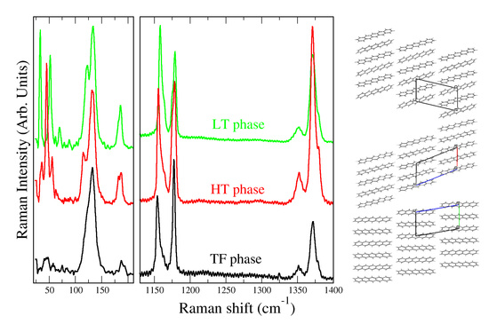
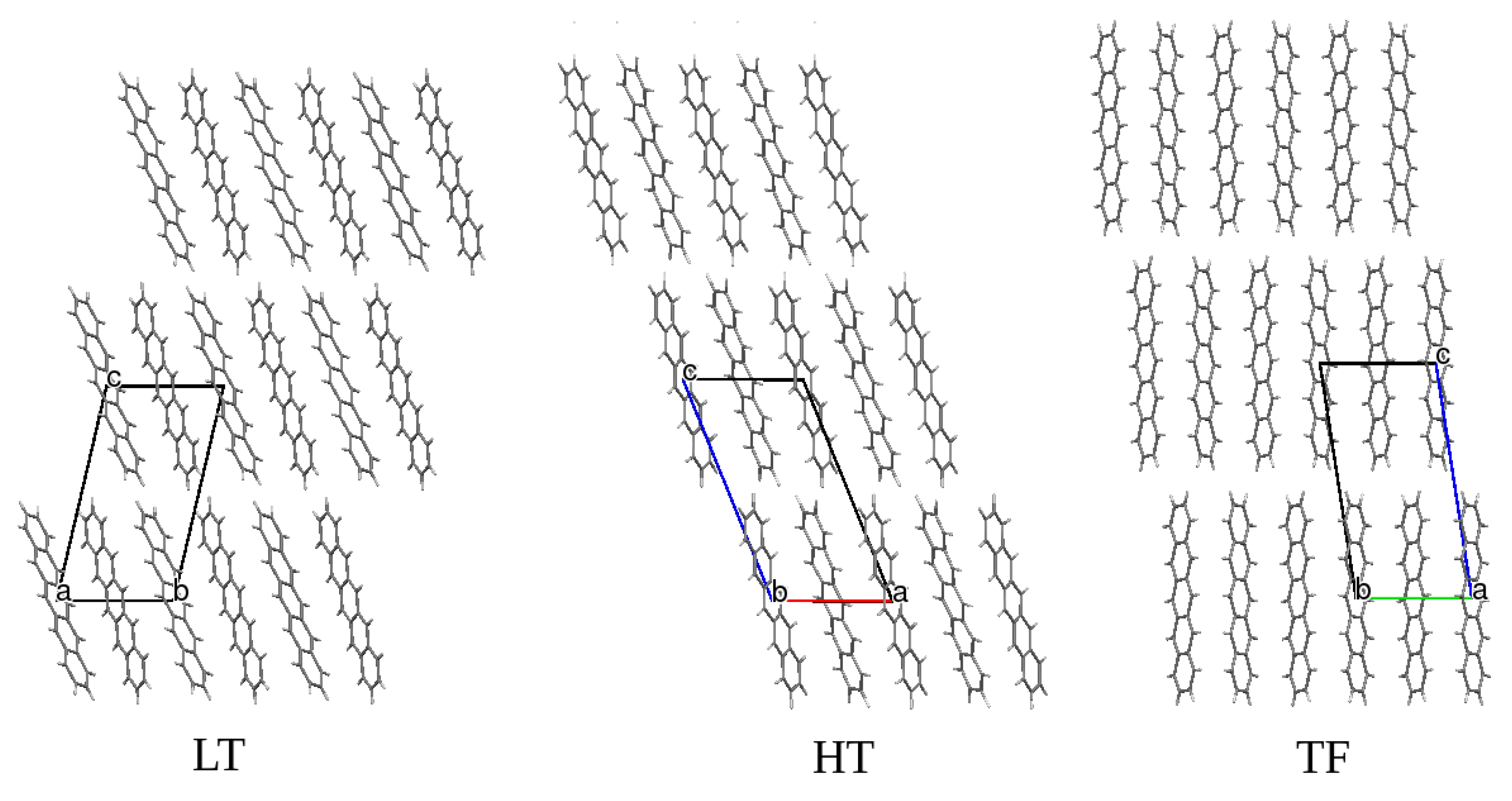
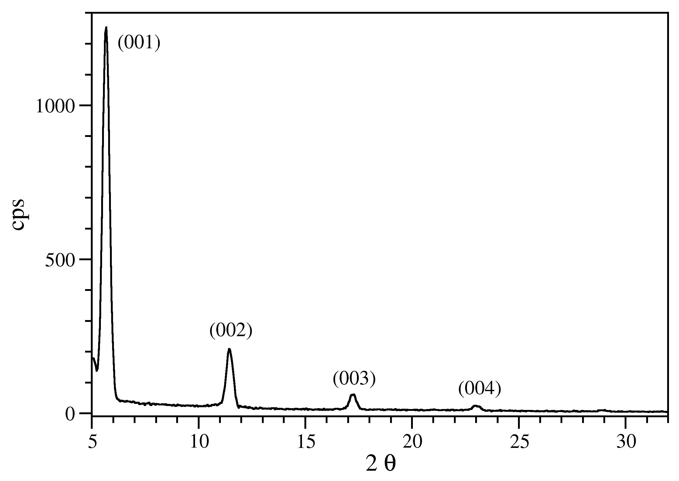
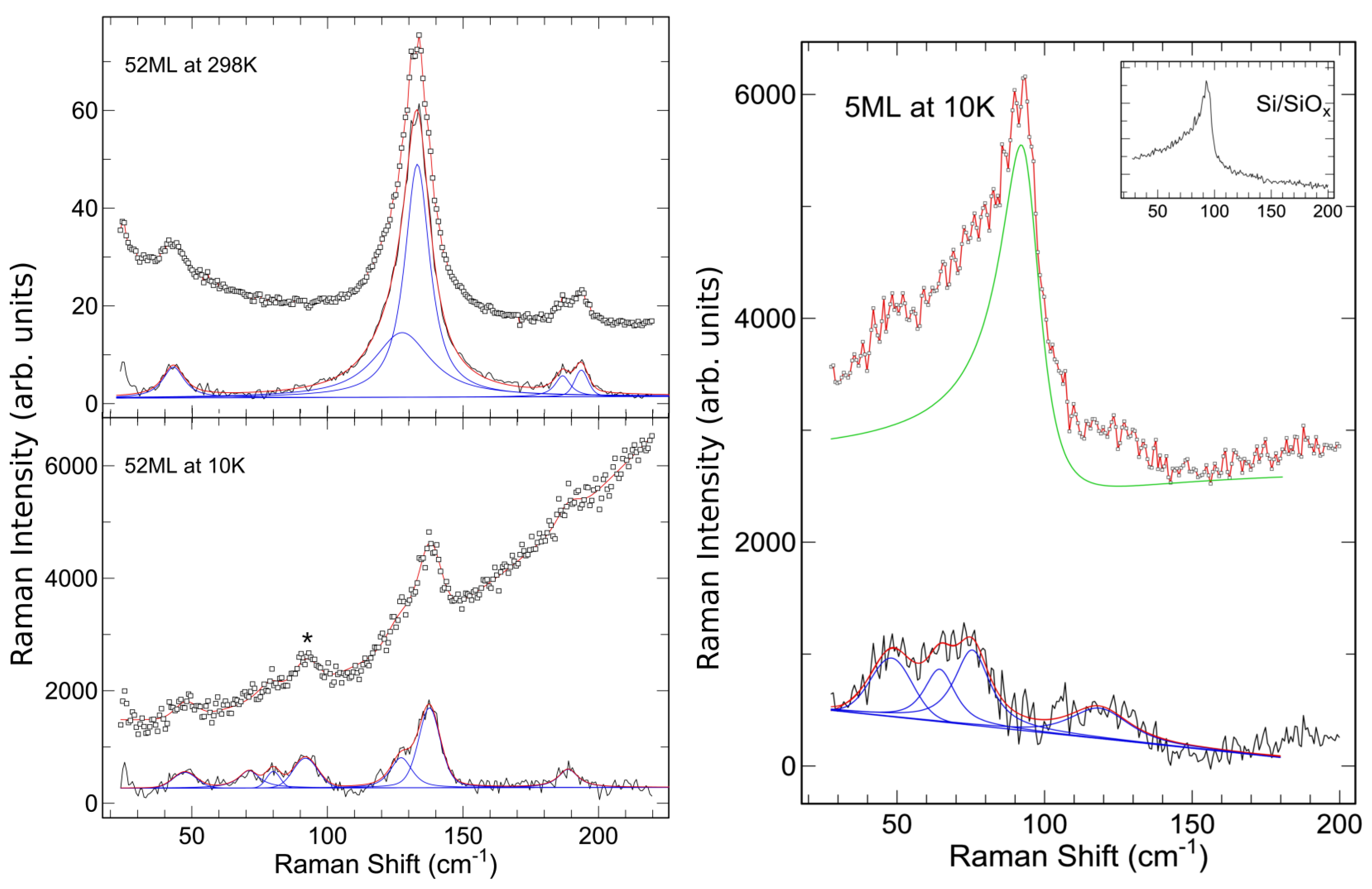
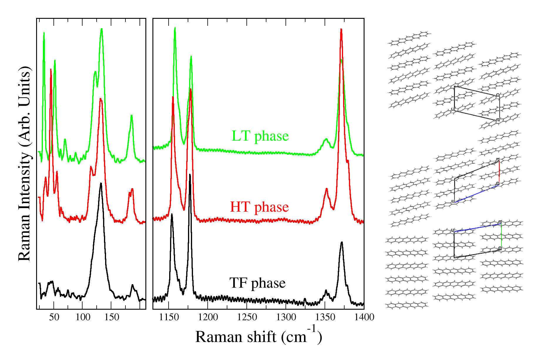
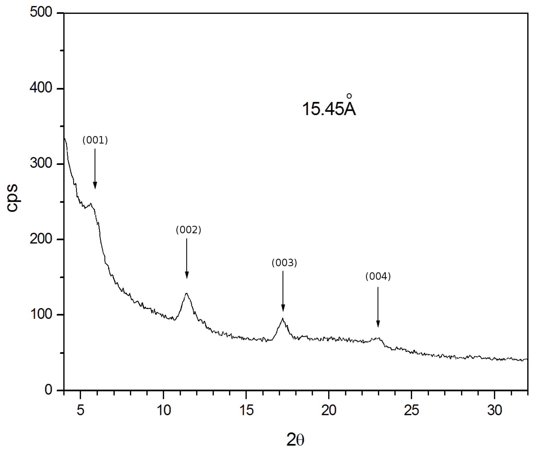
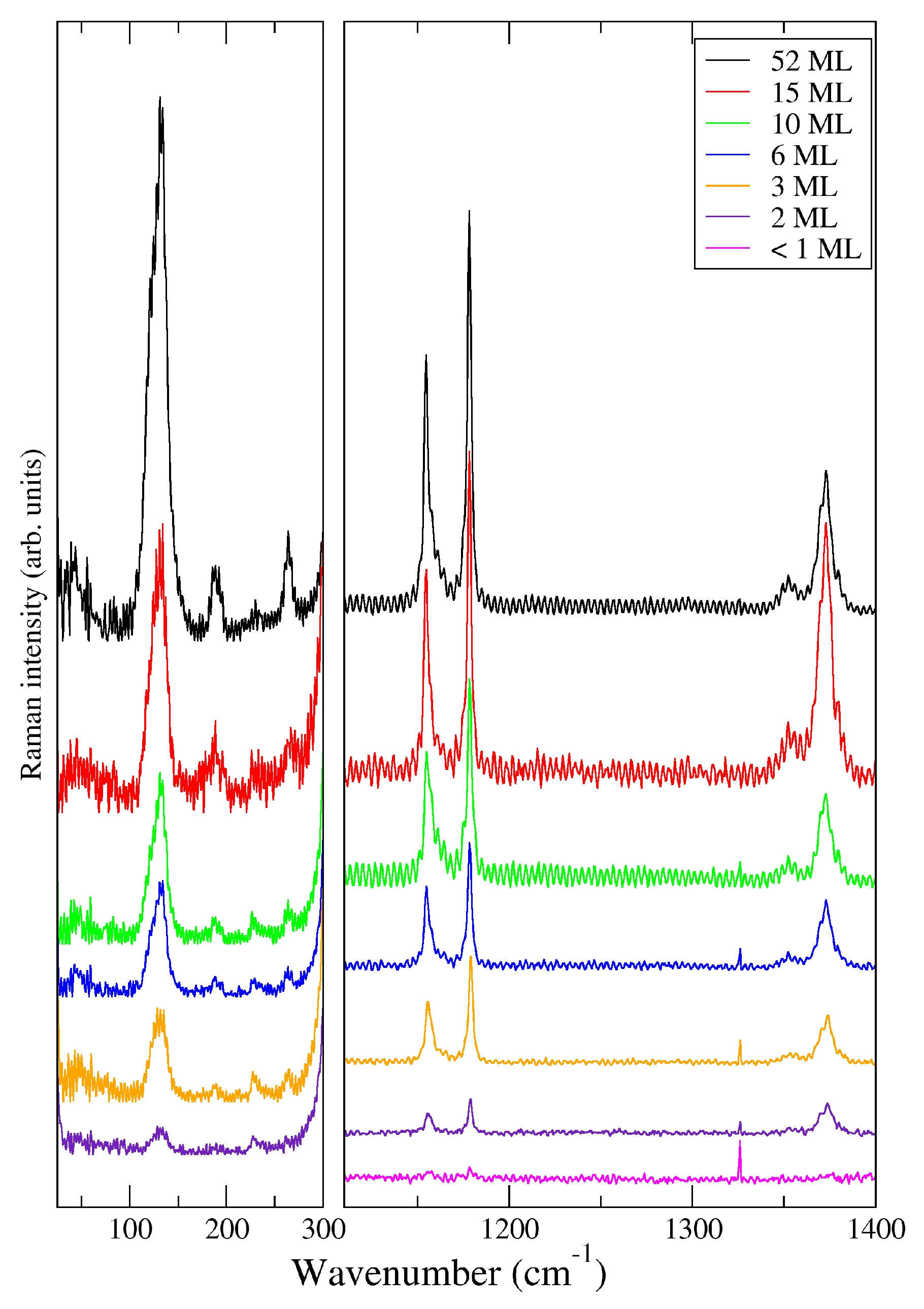
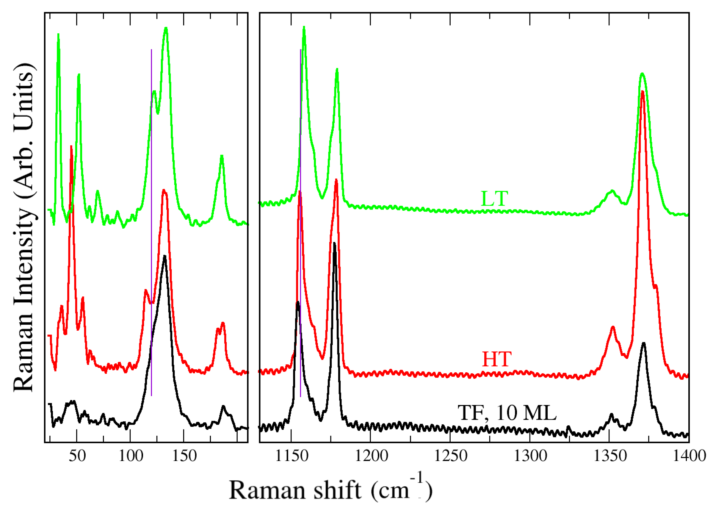
3. Results and Discussion

Figure 3 reports the Raman spectra of pentacene films grown by the SuMBD method as a function of their thickness. We report only the spectral regions of interest, namely the low frequency region, where the lattice modes are found, and the high frequency region where more subtle differences are present (see Reference [26] and below). All the spectra are collected in the same conditions (time of collection, number of scans) so the intensities can be fruitfully compared. The figure shows that the S/N of the spectra is good already for a 2 ML film. Below this thickness, much more accumulations are needed, and in the low-frequency region the signal is in any case disturbed by the scattering of the exciting line. The observed frequencies are different from those of the HT phase [26], and the band shapes remain the same up to the highest thickness, demonstrating that we are always dealing with the practically pure TF phase identified by X-ray for the 6 ML film. This is also confirmed by the frequencies in the CH bending region, which correspond to those already attributed to the TF phase [23]. As a final control, we have performed grazing angle XRD analysis on an ≈ 18 ML thick film grown by the SuMBD technique. As shown by the comparison of Figure 2 and Figure 4, the relative amount of HT phase has not increased with the film thickness.
Our SuMBD deposition method yields results different from those obtained by the conventional high-vacuum deposition: in fact, high-vacuum molecular beam deposition at a growth rate of 0.36 Ås 1 yielded TF film up to 75 ML, but with a low degree of crystallinity. Reducing the deposition rate to 0.033 Ås 1 to improve 3D order yielded films belonging to the HT phase for thickness approximately above 30 ML. Just one low-frequency spectral feature of very weak intensity, attributable to the TF phase, has been observed [23]. In our case, a lower deposition rate of about 0.008 Ås 1 (0.03 Ås 1 for the thickest film) yields highly ordered films of the TF phase up 52 ML.
The order of the films is shown by the presence since the 2 ML film of a band around 130 cm 1 , which has large character of a lattice mode [26]. The intensity of this band, compared to those of the high frequency modes, increases with the film thickness, indicating an increasing crystallinity. A more detailed discussion about the relation of the lattice phonons with film ordering will be made below.
We now focus the attention to the low-frequency lattice modes of the TF polymorph. The top left-side panel of Figure 5 shows the spectrum of the 52 ML film at room temperature. In addition to the already mentioned band around 130 cm 1 (which can be deconvoluted into 122 and 132 cm 1 bands), a weak and rather broad band at 43 cm 1 is evident. In the attempt to detect other bands, we decided to record spectra at low-temperatures. Unfortunately, at low temperature the spectra are disturbed by the tail of a strong luminescence background, whose position and intensity also depend on the number of deposited layers [31]. The effect of the luminescence is shown in the upper trace of the bottom left-side of Figure 5, representing the Raman spectra of the 52 ML TF at 10 K. After subtracting the background, some very weak bands appear below 120 cm 1 , in addition to the already mentioned broad band at 43 cm 1 , which shifts at 48 cm 1 at low T. The presence of these very weak bands is confirmed by the spectrum of the 5 ML film, shown in the right side panel of Figure 5. This figure shows that, in addition to the luminescence from pentacene, the spectrum is also disturbed by a band, of unknown origin, due to the Si/SiO x substrate (upper trace and inset of the right side panel). By subtracting the spectrum of the substrate from that of film over the substrate, we obtain the same bands as the thicker 52 ML film, but we cast doubts on the band detected there at 90 cm 1 , since it may again be due to the substrate.
The frequencies of the Raman bands observed below 140 cm 1 for the three pentacene polymorphs are collected in Table 2. The experimental frequencies are compared with the ones obtained by lattice dynamics calculations [23,26]. Although it is known that there is some degree of mixing between lattice and low-frequency intra-molecular modes [26], for the sake of clarity in the present discussion we shall use the so-called rigid molecules approximation (RMA), which provides a reasonable and intuitive description of the involved phonons. As confirmed by the calculations reported in Table 2, within the RMA the six Raman active lattice modes can be described as in-phase and out-of-phase coupling of the three librations around L (long-in-plane), M (short-in-plane) and N (normal-to-plane) molecular axes. For a perfectly ordered crystal, only the zone center, k = 0 , phonons are spectroscopically active, with frequency decreasing in the order L, M, N. In case of strong disorder, the k = 0 selection rule does not hold any more, and all the modes along the dispersion curves are active: the spectrum essentially reflects the phonon density of states, and if the mode is highly dispersive, the corresponding band may become so broad to be hardly observable. Now, the dispersion curves calculated in Reference [23] show that the highest frequency L modes are highly dispersive in the a b plane, reflecting the intermolecular interaction within the pentacene layers (see Figure 1). The fact that in our case the highest frequencies lattice modes at 122 and 132 cm 1 have intensity comparable to that of the intra-molecular modes (Figure 5) means that the films are characterized by a high degree of lateral order. This finding is in agreement with experiments showing that SuMBD-grown films grow layer by layer and have larger single crystalline domain in comparison with high-vacuum molecular beam deposition [29]. On the other hand, phonons below 80 cm 1 present dispersion along k ( 0 , 0 , k ) , i.e., normal to the a b plane [23]. These mode are still observed in our Raman spectra, but are very weak, indicating appreciable degree of disorder in the alignment between the layers.
We finally compare in Figure 6 the Raman spectra of the three pentacene polymorphs, so as to put in evidence the differences that allow to distinguish and identify them. The spectra are all unpolarized, to avoid possible confusion deriving from the different polarization of the bands [32,33]. Violet vertical lines underline the points of greater difference. As it is well known [26], the low-frequency region allows to easily distinguish the LT from the HT phase. This region is more difficult to use to identify the TF polymorph, because disorder broadens or washes out the bands. If the spectrum is at least partially observed, as in our case, the difference is more pronounced with respect to the LT polymorph in comparison with the HT one. On the other hand, the right side of Figure 6 demonstrates that the subtle differences in the CH bending frequency region allow not only to distinguish the LT from the HT phase, but also separates the TF one from the other two. In fact, the peak frequency of the band around 1150–1160 cm 1 occurs at 1154, 1156 and 1158 cm 1 for the TF, HT and LT polymorph, respectively, and also the band shape is different. Since precise calibration of the Raman frequency shifts is often delicate, we suggest to rather use the frequency difference with respect to the band around 1370 cm 1 , which is in the order 217, 214 and 213 cm 1 .

4. Conclusions

In this paper, we have once more demonstrated that Raman micro-spectroscopy is a very efficient and non-destructive method to characterize different polymorphs of organic semiconductors. In addition, the comparison between the spectral region of lattice phonons with that of the intra-molecular vibrations provides useful insights on the degree of crystallinity of the studied compound, pentacene. Indeed, the fact that intensity of the bands around 130 cm 1 is of the same order of magnitude of that of intramolecular bands shows that the TF phase grown by SuMBD method has an high degree of lateral order, i.e., the film grows layer-by-layer up to the highest obtained thickness, 52 ML. However, the interlayer correlation is low, as shown by the weakness of the lowest frequency Raman phonons. From this point of view, the TF phase can by considered as a sort of two-dimensional (2D) phase, i.e., long range order can exist only in the a b plane, whereas the HT (or LT) phase is a true 3D phase, even when grown in the form of film. This is confirmed by the fact that low-rate high-vacuum molecular beam deposition yield 3D nucleation, finally ending in a (disordered) HT polymorph, with all the 3D lattice phonons being clearly visible [23].

Acknowledgments

Work at Parma and Bologna Universities has been supported by the Italian Ministry of University and Research (M.I.U.R.) under the project PRIN-2010ERFKXL.

Author Contributions

Alberto Girlando, Aldo Brillante and Salvatore Iannotta coordinated the team work and contributed in the data interpretation. Tullio Toccoli has prepared and characterized the films, Matteo Masino has obtained the Raman spectra.

Conflicts of Interest

The authors declare no conflict of interest.

References

  1. Dimitrakopoulos, C.D.; Malenfant, P.R.L. Organic Thin Film Transistors for Large Area Electronics. Adv. Mater. 2002, 14, 99–117. [Google Scholar] [CrossRef]
  2. Dong, H.; Fu, X.; Liu, J.; Wang, Z.; Hu, W. 25th Anniversary Article: Key Points for High-Mobility Organic Field-Effect Transistors. Adv. Mater. 2013, 25, 6158–6183. [Google Scholar] [CrossRef] [PubMed]
  3. Jurchescu, O.D.; Baas, J.; Palstra, T.T.M. Effect of impurities on the mobility of single crystal pentacene. Appl. Phys. Lett. 2004, 84, 3061–3063. [Google Scholar] [CrossRef]
  4. Jurchescu, O.D.; Mourey, D.A.; Subramanian, S.; Parkin, S.R.; Vogel, B.M.; Anthony, J.E.; Jackson, T.N.; Gundlach, D.J. Effect of polymorphysm on charge transport in organic semiconductors. Phys. Rev. B 2009, 80, 085201. [Google Scholar] [CrossRef]
  5. Brillante, A.; Bilotti, I.; Della Valle, R.G.; Venuti, E.; Masino, M.; Girlando, A. Characterization of phase purity in organic semiconductors by lattice phonons confocal Raman mapping: Application to pentacene. Adv. Mater. 2005, 17, 2549–2553. [Google Scholar] [CrossRef]
  6. Venuti, E.; Della Valle, R.G.; Brillante, A.; Masino, M.; Girlando, A. Probing Pentacene Polymorphs by Lattice Dynamics Calculations. J. Am. Chem. Soc. 2002, 124, 2128–2129. [Google Scholar] [CrossRef] [PubMed]
  7. Ruiz, R.; Choudhary, D.; Nickel, B.; Toccoli, T.; Chang, K.C.; Mayer, A.C.; Clancy, P.; Blakely, J.M.; Headrick, R.L.; Iannotta, S.; et al. Pentacene Thin Film Growth. Chem. Mater. 2004, 16, 4497–4508. [Google Scholar] [CrossRef]
  8. Duffy, C.M.; Andreasen, J.W.; Breiby, D.W.; Nielsen, M.M.; Ando, M.; Minakata, T.; Sirringhaus, H. High-Mobility Aligned Pentacene Films Grown by Zone-Casting. Chem. Mater. 2008, 20, 7252–7259. [Google Scholar] [CrossRef]
  9. Della Valle, R.G.; Venuti, E.; Brillante, A.; Girlando, A. Molecular dynamics simulations for a pentacene monolayer on amorphous silica. ChemPhysChem 2009, 10, 1783–1788. [Google Scholar] [CrossRef] [PubMed]
  10. Yoneya, M.; Kawasaki, M.; Ando, M. Molecular dynamics simulations of pentacene thin films: The effect of surface on polymorph selection. J. Mater. Chem. 2010, 20, 10397–10402. [Google Scholar] [CrossRef]
  11. Holmes, D.; Kumaraswamy, S.; Matzger, A.J.; Vollhardt, K.P. On the Nature of Nonplanarity in the [N]Phenylenes. Chem. Eur. J. 1999, 5, 3399–3412. [Google Scholar] [CrossRef]
  12. Mattheus, C.C.; Dros, A.B.; Baas, J.; Meetsma, A.; de Boer, J.L.; Palstra, T.T.M. Polymorphism in pentacene. Acta Cryst. 2001, C57, 939–941. [Google Scholar] [CrossRef]
  13. Siegrist, T.; Kloc, C.; Schön, J.H.; Batlogg, B.; Haddon, R.C.; Berg, S.; Thomas, G.A. Enhanced Physical Properties in a Pentacene Polymorph. Angew. Chem. Int. Ed. 2001, 40, 1732–1736. [Google Scholar] [CrossRef]
  14. Campbell, R.B.; Roberston, J.M.; Trotter, J. The crystal and molecular structure of pentacene. Acta Crystallogr. 1962, 14, 705–711. [Google Scholar] [CrossRef]
  15. Farina, L.; Brillante, A.; Della Valle, R.G.; Venuti, E.; Amboage, M.; Syassen, K. Pressure-induced phase transition in pentacene. Chem. Phys. Lett. 2003, 375, 490–494. [Google Scholar] [CrossRef]
  16. Siegrist, T.; Besnard, C.; Haas, S.; Schiltz, M.; Pattison, P.; Chernyshov, D.; Batlogg, B.; Kloc, C. A Polymorph Lost and Found: The High-Temperature Crystal Structure of Pentacene. Adv. Mater. 2007, 19, 2079–2082. [Google Scholar] [CrossRef]
  17. Chou, W.-Y.; Chang, M.-H.; Cheng, H.-L.; Lee, Y.-C.; Chang, C.-C.; Sheu, H.-S. New Pentacene Crystalline phase Induced by Nanoimprinted Polyimide Gratings. J. Phys. Chem. C 2012, 116, 8619–8626. [Google Scholar] [CrossRef]
  18. Cheng, H.L.; Mai, Y.S.; Chou, W.Y.; Chang, L.R.; Liang, X.W. Thickness-dependent structural evolution and growth models in relation to carrier transport properties in polycrystalline pentacene films. Adv. Funct. Mater. 2007, 17, 3639–3649. [Google Scholar] [CrossRef]
  19. Mattheus, C.C.; Dros, A.B.; Baas, J.; Oostergetel, G.T.; Meetsma, A.; de Boer, J.L.; Palstra, T.T.M. Identification of polymorphs of pentacene. Synth. Met. 2003, 138, 475–481. [Google Scholar] [CrossRef] [Green Version]
  20. Schiefer, S.; Huth, M.; Dobrinevski, A.; Nickel, B. Determination of the Crystal Structure of Substrate-Induced Pentacene Polymorphs in Fiber Structured Thin Films. J. Am. Chem. Soc. 2007, 129, 10316–10317. [Google Scholar] [CrossRef] [PubMed]
  21. Drummy, L.F.; Martin, D.C. Thickness-Driven Orthorhombic to Triclinic Phase Transformation in Pentacene Thin Films. Adv. Mater. 2005, 17, 903–907. [Google Scholar] [CrossRef]
  22. Mannsfeld, S.C.B.; Virkar, A.; Reese, C.; Toney, M.F.; Bao, Z. Precise Structure of Pentacene Monolayers on Amorphous Silicon Oxide and Relation to Charge Transport. Adv. Mater. 2009, 21, 2294–2298. [Google Scholar] [CrossRef]
  23. Brillante, A.; Bilotti, I.; Della Valle, R.G.; Venuti, E.; Girlando, A.; Masino, M.; Liscio, F.; Milita, S.; Albonetti, C.; D’Angelo, P.; et al. Structure and dynamics of pentacene on SiO2 : From monolayer to bulk structure. Phys. Rev. B 2012, 85, 195308. [Google Scholar] [CrossRef]
  24. Ando, M.; Kehoe, T.B.; Yoneya, M.; Ishii, H.; Kawasaki, M.; Duffy, C.M.; Minakata, T.; Phillips, R.T.; Sirringhaus, H. Evidence for Charge-Trapping Inducing Polymorphic Structural-Phase Transition in Pentacene. Adv. Mater. 2015, 27, 122–129. [Google Scholar] [CrossRef] [PubMed]
  25. Brillante, A.; Bilotti, I.; Della Valle, R.G.; Venuti, E.; Girlando, A. Probing polymorphs of organic semiconductors by lattice phonon Raman microscopy. CrystEngComm 2008, 10, 937–946. [Google Scholar] [CrossRef]
  26. Brillante, A.; Della Valle, R.G.; Farina, L.; Girlando, A.; Masino, M.; Venuti, E. Raman phonon spectra of pentacene polymorphs. Chem. Phys. Lett. 2002, 357, 32–36. [Google Scholar] [CrossRef]
  27. He, R.; Tassi, N.G.; Blanchet, G.B.; Pinczuk, A. Low-lying lattice modes of highly uniform pentacene monolayers. Appl. Phys. Lett. 2009, 94, 223310. [Google Scholar] [CrossRef]
  28. Wong, F.; He, R.; Pinkzuk, A. An Optical and Structural Study of Pentacene Thin-film Polymorphs. Columbia Undergrad. Sci. J. 2006, 1, 50–55. [Google Scholar]
  29. Wu, Y.; Toccoli, T.; Koch, N.; Iacob, E.; Pallaoro, A.; Rudolf, P.; Iannotta, S. Controlling the Early Stages of Pentacene Growth by Supersonic Molecular Beam Deposition. Phys. Rev. Lett. 2007, 98, 076601. [Google Scholar] [CrossRef] [PubMed]
  30. Gottardi, S.; Toccoli, T.; Wu, Y.; Iannotta, S.; Rudolf, P. Growth dynamics in supersonic molecular beam deposition of pentacene sub-monolayers on SiO2. Chem. Commun. 2014, 50, 7694–7697. [Google Scholar] [CrossRef] [PubMed]
  31. He, R.; Tassi, N.G.; Blanchet, G.B.; Pinczuk, A. Intense photoluminescence from pentacene monolayers. Appl. Phys. Lett. 2010, 96, 263303. [Google Scholar] [CrossRef]
  32. Stenger, I.; Frigout, A.; Tondelier, D.; Geffroy, B.; Ossikovski, R.; Bonassieux, Y. Polarized micro-Raman spectroscopy of pentacee thin-film. Appl. Phys. Lett. 2009, 94, 133301. [Google Scholar] [CrossRef]
  33. Cheng, H.-L.; Liang, X.-W.; Chou, W.-Y.; Mai, Y.-S.; Yang, C.-Y.; Chang, L.-R.; Tang, F.-C. Raman spectroscopy applied to reveal polycrystalline grain structures and carrier transport properties of organic semiconductors films: Application to pentacene-based organic transistors. Org. Electr. 2009, 10, 289–298. [Google Scholar] [CrossRef]
Figure 1. Structure of the low temperature (LT), high temperature (HT) and thin-film (TF) polymorphs of pentacene.
Crystals 06 00041 g001
Figure 2. Grazing angle X-ray diffraction pattern of the 2010-017, 6 ML pentacene film.
Crystals 06 00041 g002
Figure 3. Raman spectra of pentacene films as a function of thickness (in ML). Only the spectral regions of interest are reported.
Crystals 06 00041 g003
Figure 4. Grazing angle X-ray diffraction pattern for a ≈ 18 ML pentacene film.
Crystals 06 00041 g004
Figure 5. Left panels: Low-frequency Raman spectra of the 52 ML pentacene TF, at 298 K (top) and at 10 K (bottom). In both cases the upper curves are the raw experimental data, and the lower ones the data after fluorescence background subtraction. Spectral deconvolution is also shown as thin blue lines. The band marked with an asterisk might be due to the substrate. Right panel: Low-frequency Raman spectra of 5 ML pentacene TF at 10 K. Inset: Raman spectrum of the substrate alone. The upper curve is the spectrum, with overimposed in green the curve fitting of the inset Si/SiO x spectrum. The lower curve is the spectrum after substrate spectrum subtraction, with the corresponding deconvolution (thin blue lines).
Crystals 06 00041 g005
Figure 6. Low- and high-frequency unpolarized Raman spectra of the three pentacene polymorphs. The spectra are offset for clarity.
Crystals 06 00041 g006
Table 1. Characterization of the obtained pentacene films. The thickness in ML (monolayers) assumes 1 ML ≃ 15 Å.
LabelThickness (Å)Thickness (ML)
10-02781 ± 1552
10-01226 ± 515
10-016145 ± 310
10-01788.2 ± 2.86
10-01880.8 ± 2.65
10-01949.2 ± 2.93
10-02023.0 ± 1.6∼1–2
10-02111–12<1
Table 2. Room temperature experimental frequencies (cm 1 ) of the three pentacene polymorphs, compared with the k = 0 frequencies calculated in the rigid molecule approximation at potential energy minimum.
Pentacene TFPentacene HTPentacene LT
Expt.Calc. a Expt.Calc. a Expt.Calc. b
30.436.446.733.133.5
43.244.545.557.252.264.1
70.0 c 70.755.775.569.876.9
88.5 115.088.1110.2
122.3133.8115.1155.8122.5157.9
132.3140.8132.3164.8133.2164.1
a Reference [26]; b Reference [23]; c 10 K.

