Article

E’’ Raman Mode in Thermal Strain-Fractured CVD-MoS2

1
Hunan Key Laboratory of Super-Microstructure and Ultrafast Process, School of Physics and Electronics, Central South University, Changsha 410083, China
2
State Key Laboratory of Powder Metallurgy, Central South University, Changsha 410083, China
3
College of Physics and Microelectronics, Hunan University, Changsha 410082, China
4
Department of Physics and Astronomy, University of Rochester, Rochester, NY 14627, USA
*
Author to whom correspondence should be addressed.
Crystals 2016, 6(11), 151; https://doi.org/10.3390/cryst6110151
Submission received: 10 October 2016 / Revised: 11 November 2016 / Accepted: 14 November 2016 / Published: 18 November 2016

Abstract

:
Molybdenum disulfide (MoS2) has recently attracted considerable interests due to its unique properties and potential applications. Chemical vapor deposition (CVD) method is used widely to grow large-area and high-quality MoS2 single crystals. Here, we report our investigation on thermal strain-fractured (SF) single crystalline MoS2, oxidation-fractured MoS2, and normal MoS2 by atomic force microscopy (AFM), Raman and photoluminescence (PL) measurements. Several new Raman modes are observed for SF-MoS2. The band gap of SF-MoS2 is enlarged by 150 meV and the PL intensity is reduced substantially. These results imply that a structural transformation occurs in SF-MoS2. Our findings here are useful for the design of MoS2-based nanocatalysts with relative high catalytic activity.

Graphical Abstract

1. Introduction

Since the isolation of graphene, two-dimensional (2D) materials have gained great developments in the past decade [1,2]. Transition metal dichalcogenides (TMDCs) have attracted much attention due to their exotic physical and chemical properties as well as potentials in electronic and photonic applications [3,4]. 2D TMDCs chemical formula is MX2 where M represents a transition metal element (such as Mo, W) and X represents a chalcogen element (S, Se and Te). Among TMDCs, MoS2 has been studied in a wide range. While bulk MoS2 comprises of 2D S-Mo-S layers stacked by van der Waals interactions, single layer MoS2 comprises a Mo layer sandwiched between two S layers by covalent interactions [5]. Compared with graphene, MoS2 provides an intrinsic bandgap that is essential to the preparation of high-performance digital integrated circuits. With the decreasing of thickness, the corresponding bandgap transforms from indirect one of ~1.2 eV for bulk MoS2 to a direct one of ~1.9 eV for single layered MoS2, due to the quantum confinement effect [6]. Additionally, single layered MoS2 has a high charge carrier mobility over 220 cm2/VS and an on/off ratio of 108 [6]. Single layered MoS2-based phototransistor exhibits a photoresponsivity up to 880 A/W at a wavelength of 561 nm, which is superior to graphene-based devices with a similar geometry [7]. Moreover, single layered MoS2 exhibits outstanding mechanical properties [8,9]. The Young’s modulus of suspended single layered MoS2 is ~270 GPa, which is higher than that of stainless steel [10,11]. Therefore, MoS2 possesses excellent potential application in field effect transistors (FETs), optoelectronic and flexible devices [6,7,12].
MoS2 exhibits several different polymorphs, which yield different properties. Among them, 2H-MoS2 (labeled as 1H in single layered MoS2) with a trigonal prismatic unit cell is semiconducting and 1T/1T’ phases with an octahedral unit cell (twisted octahedral in the 1T’ phase) is metallic [13]. Figure 1 shows the unit cell of such two phases, respectively. Therefore, engineering the phase of MoS2 contributes to its applications in catalysts and optoelectronic devices [14]. Bulk 2H-MoS2 can be transformed into 1T/1T’-MoS2 by lithium intercalation to accommodate the transferred charges from Li atoms [15,16]. However, the 1T/1T’ phase is metastable and would transfer back to 2H-MoS2 with aging. Single layered MoS2 undergoes similar phase transition from 1H to 1T/1T’ when bombarded by electrons [13].
It is well known that the amount of catalytic active sites along the edges of MoS2 is one of the key factors for the hydrogen evolution reaction (HER). It is enhanced heavily by growing MoS2 thin films with vertically aligned layers in previous reports [17,18]. Recently, Our group reported the underlying formation mechanism of SF-MoS2 [19], where the number of edges increased heavily [14,20]. However, the structural and vibrational properties of such SF-MoS2 have not been investigated yet. In this article, for comparison, we used AFM, Raman and PL spectroscopy/imaging to investigate three kinds of single layered MoS2 specimens: the normal one (1H), the oxidation-fractured (OF) one and the SF one. For SF-MoS2, the two characteristic PL peaks blue shift by 150 meV compared with the normal specimen. In addition to the E’ and A’1 modes in Raman spectra, one additional mode at 289.3 cm−1 is observed, which should be forbidden for 1H-MoS2 in a setup with backscattering geometry due to the lack of inversion symmetry [21]. Our findings here are useful for the design of MoS2-based nanocatalysts with relative high catalytic activity.

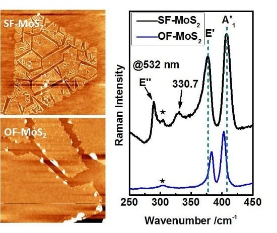
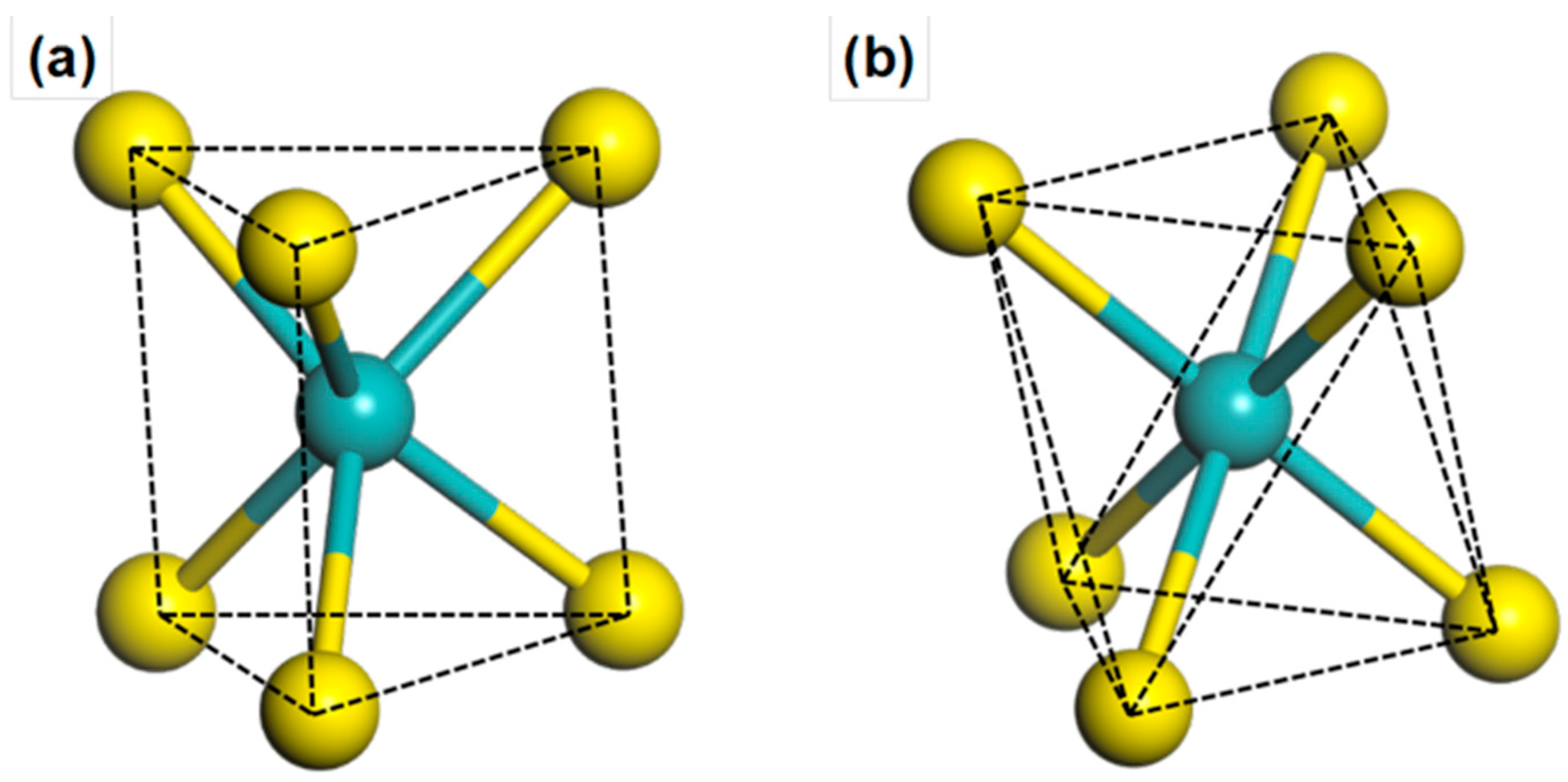
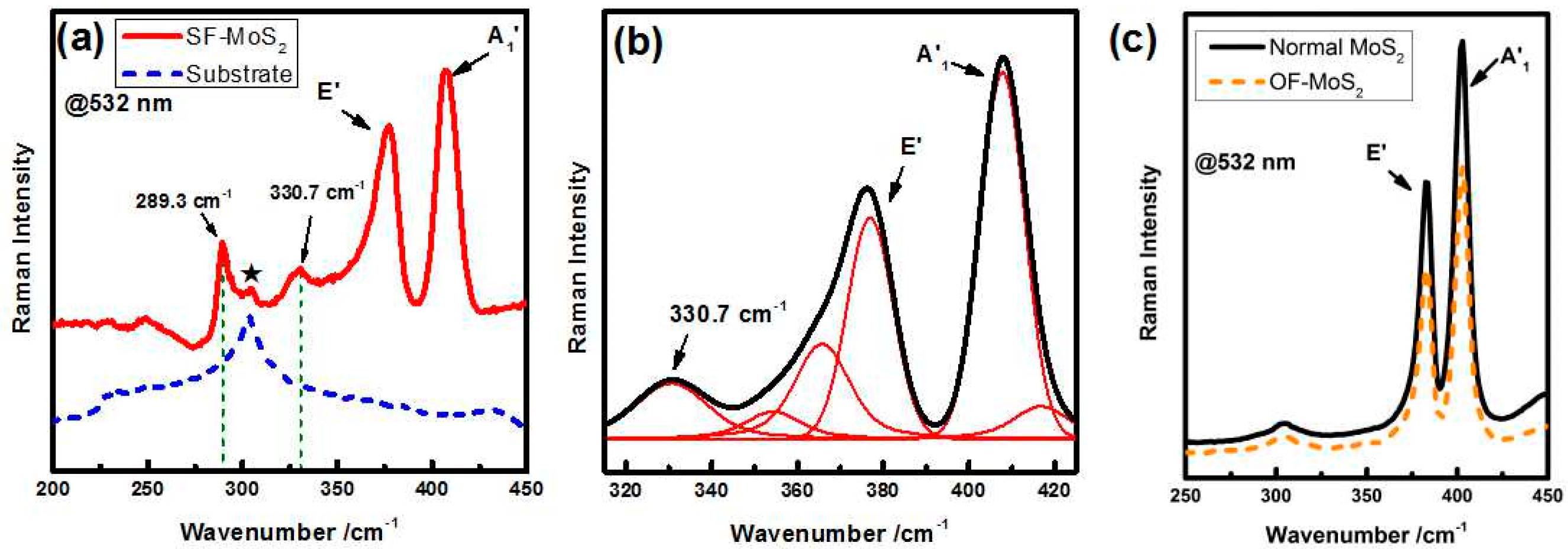
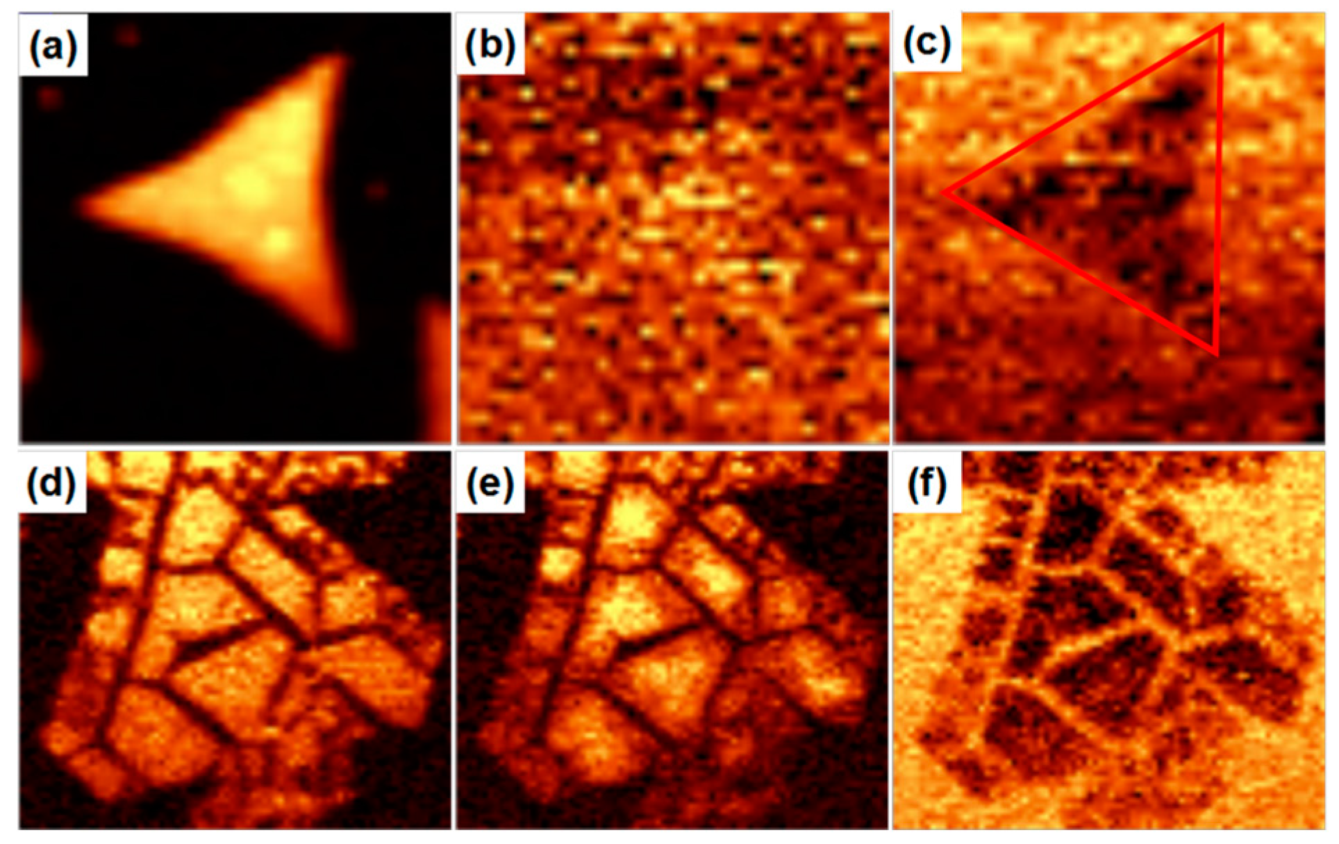
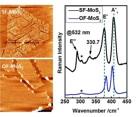
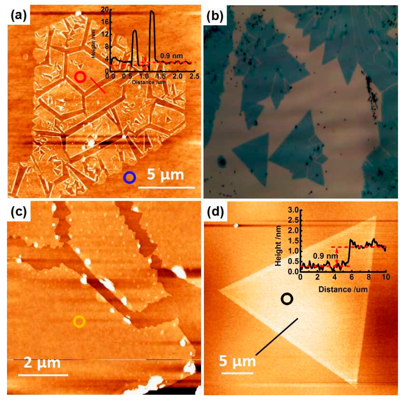
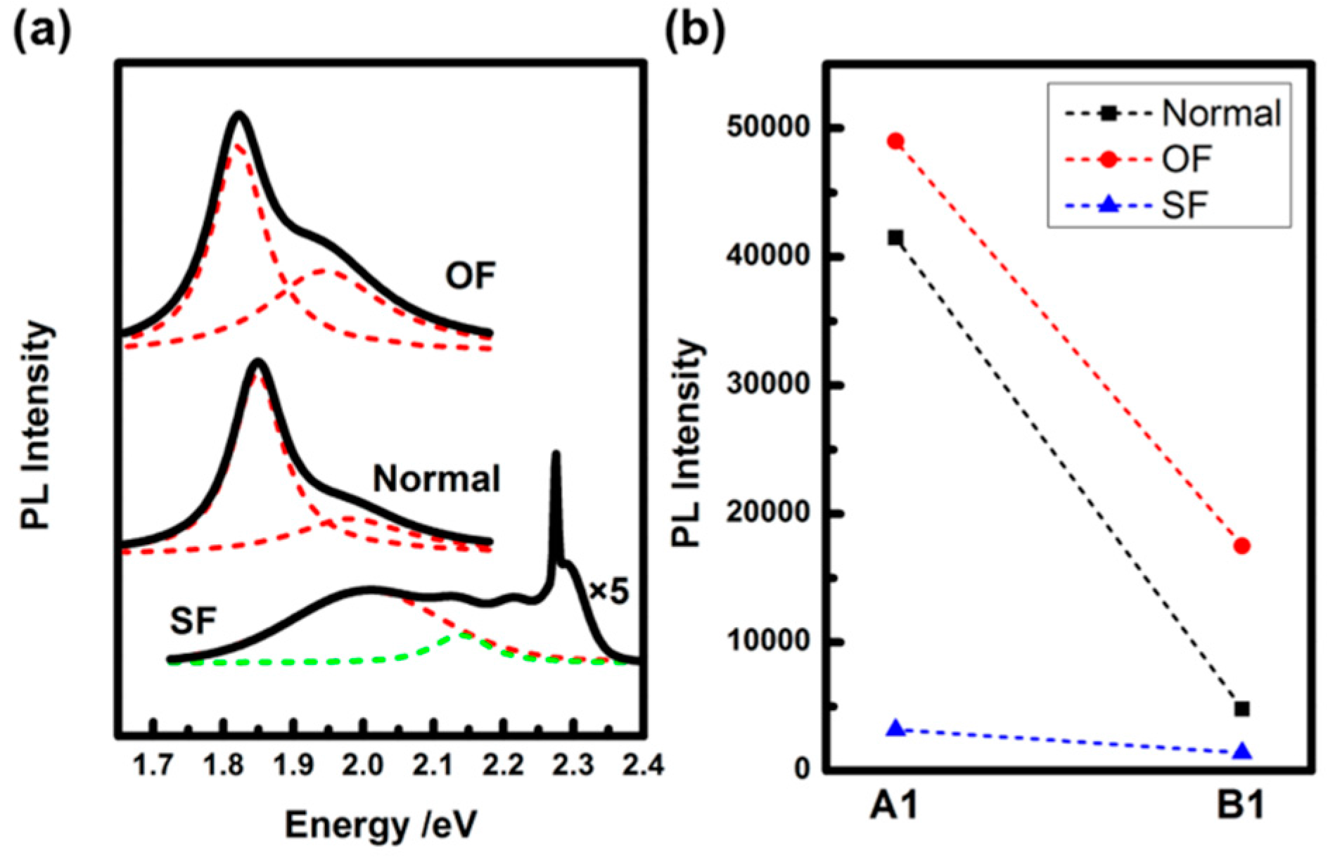
2. Result and Discussion

Figure 2a shows a representative AFM image of the SF-MoS2. Some cracks were observed. The cracks in 1H-MoS2 with three-fold symmetry tend to propagate along the crystallographic directions of <10-10>, which has weak bond strengths. The thermal expansion coefficient of MoS2 (10−5/°C) is ~1000 times as large as that of silicon dioxide (5.6 × 10⁻⁸/°C) [22]. The cooling rate is up to ~280 °C/min according to the standard non-stationary heat exchange Equation (1) (For details, please refer to the Experimental Details section). Thus, thermal strain cannot be released sufficiently during the fast quenching process at the end of CVD synthesis process. Apparently, these behaviors differ from oxidation-induced intergranular fracture behaviors in MoS2 [23,24]. The inset height profile along solid red line in Figure 2a presents the height of SF-MoS2 of ~0.9 nm. It is slightly higher than the height of ~0.7 nm for the micromechanically exfoliated single layered MoS2 [25], but much lower than the height of ~1.4 nm for bilayer MoS2 [26]. It is worth noting that the measured heights at the edges of fractured microflake are ~14 and ~20 nm, and located around the cracks, indicating that MoS2 curls into nanoscrolls rather than folds back into bilayer one [19]. Thus, besides of the edges, the center of micro flake maintains single layered.
Figure 2b displays a representative OM image of OF-MoS2, showing that fracture only occurs along the grain boundaries between single crystalline MoS2 domains due to their higher chemical reactivity. This is similar to the case of WS2 annealing under ambient condition [23]. The local AFM image in Figure 2c shows the edge of single layered OF-MoS2 in the flat and smooth zigzag facets instead of nanoscolls. In fact, the intergranular fracture behaviors of OF-MoS2 are arisen from the oxygen induced etching during the end of the synthesis process. OF-MoS2 has the triangle island in Figure 2b, indicating its structure is like 1H-MoS2. Figure 2d presents the AFM image of normal MoS2 in the shape of equilateral triangle. The inset height profile scan along solid black line in Figure 2d indicates single layer.
PL measurements were carried out for the three kinds of specimens. The PL spectra of normal, OF- and SF-MoS2 are shown in Figure 3a. Two prominent peaks located at 1.98 (B1) and 1.85 (A1) eV corresponding to the direct excitonic transition between the minimum of the conduction band and the splitting valence bands at the K point are observed for normal MoS2 [25]. Both peaks are observed on OF-MoS2 with slight red shift of 30 meV due to the different residual strains.
For the PL spectrum of SF-MoS2 (the bottom one in Figure 3a), except for the two peaks located at 2.22 and 2.28 eV which are assigned to the first and second order Raman modes from the silicon substrate, two other components located at 2.13 (B1) and 2.00 (A1) eV are required to fit it [27]. The energy difference of 130 meV is the same as that of normal and OF-MoS2. Thus, we assign them to the characteristic excitonic peaks. Both peaks blue shift by 150 meV, indicating that the bandgap is enlarged by 150 meV. The d orbitals of Mo atoms, which contributes to the direct K-K interband transition between the conduction band minimum (CBM) and valence band maximum (VBM) at the K point in the Brillouin zone, may moves away from Fermi level and lead to an increase in the band gap with the compressive stress increases [28]. Thus, a compressive stress may exist in SF-MoS2, which may result in the base plane shrink following fracturing. Figure 3b summarizes the PL intensities of these samples. It is reported that the PL intensity of A1 peak is enhanced by six (eighty nine) times when O2 is absorbed physically (chemically) on the MoS2 surface [24]. The A1 peak intensity ratio between OF- and normal MoS2 is ~1.2, indicating no obvious O2 chemically absorbed on the basal plane of OF-MoS2 during the CVD process at the annealing temperature of ~400 °C and in N2 atmosphere with small amount of O2, unlike the previously reported annealing results under ambient conditions [24]. The intensities of both PL peaks from SF-MoS2 decrease heavily. We consider that the smaller difference of the intensities is attributed to no obvious O2 chemically absorbed on the basal plane of OF-MoS2 [24]. Therefore, such transgranular fracture behavior can be mainly attributed to thermal stress. Pressure-induced intralayer hybridization between Mo d orbitals and S p orbitals may lead to a crossover from direct to indirect transition and to PL quenching [29,30]. Defects and metallic nature also lead to PL quenching [24,28]. With the increasing concentration of S vacancies, the exciton absorption intensity decreases. The increasing of nonradiative rate of electron-hole recombination also results in the PL quenching [31].
To further investigate the vibrational properties of SF-MoS2, Raman measurements were carried out. For bulk MoS2, there are three characteristic Raman modes corresponding to E12g, A1g and E1g modes. A change of crystal symmetry leads the notation of these modes to E’ (~384.7 cm−1), A’1 (~405.0 cm−1) and E’’ (~286.0 cm−1) for single layered MoS2 [21,32]. Figure 4a presents the Raman spectra excited by 532 nm laser from SF-MoS2 (red solid curve) and bare SiO2/Si substrate (blue dotted curve) at room temperature at ambient. Two prominent Raman modes corresponding to E’ and A’1 modes are observed only on the fractured features, confirming that the fractured sample is MoS2. Both modes are broadening heavily. In the case of first order Raman scattering in a pristine sample, the momentum conservation dictates that only phonons near the Brillouin zone center, Γ, can be involved in the process. The out-of-plane optical (ZO) branch leads to the A’1 mode. The longitudinal optical (LO) and transverse optical (TO) branches give rise to the degenerated E’ mode with a small LO-TO splitting (<3 cm−1). However, for a defective system, Raman modes involving phonons at the zone edge of the first Brillouin zone, M, can be activated by the momentum contribution of a defect without violating wave-vector conservation [15,33]. Figure 4b shows the fitting of E’ and A’1 modes. Due to the effect of phonon confinement, one (two) defect-induced Raman mode(s) at ~416.8 cm−1 (354.3 and 365.7 cm−1), which overlaps with the A’1 (E’) mode, can be assigned to the ZO (TO and LO) branch at the M point [33]. The appearance of defect-induced modes at the low-wavenumber region of the Raman spectrum (100–270 cm−1) of SF-MoS2 is shown in Figure S2. The Raman mode at 330.7 cm−1 in Figure 2b is also ascribed to zone-edge scattering by the defects [15]. These results imply that the mode broadening may be caused by the defects.
In comparison with normal CVD-MoS2 [33], E’ mode has a red shift of ~7.8 cm−1 while A’1 mode has a blue shift of ~2.8 cm−1. The wavenumber difference between E’ and A’1 modes of SF-MoS2 is 30.9 cm−1, which is much larger than previous reported of ~20.3 cm−1 for single layered CVD-MoS2 and ~24.8 cm−1 for bulk MoS2 [32,34]. Many factors such as doping, strains and defects will result in the mode shifting and broadening [35,36]. With the increasing of electronic doping level, the A’1 mode will have a red shift, accompanied by an increase in the line width of its Raman mode [37]. Upon compression, both E’ and A’1 modes of single layered MoS2 show an apparent blue shift and broadening due to the increasing of the interaction between atoms [28]. Theoretically, with the increasing of sulfur vacancies concentration (Vs) in 1H-MoS2, the wavenumber difference between E’ and A’1 modes increase obviously. When Vs increases from 0% to 50%, the wavenumber of E12g mode is decreased by 100.6 cm−1 while A1g mode is increased by 42.3 cm−1 [38]. Experimentally, a similar evolution is observed in single layered MoS2 either bombarded by manganese ion (Mn+) [33] or treated by oxygen plasma [31]. When the defect density reaches up to 1/nm2, the wavenumber difference between E12g and A1g modes increases to 26 ± 4 cm−1 [33]. The large wavenumber difference of ~30.9 cm−1 indicates that sulfur vacancies, which may serve as crack nuclei in SF-MoS2, exist widely in SF-MoS2 flakes [39]. This is in agreement with the results of X-ray photoelectron spectroscopy (XPS) [19].
Interestingly, one additional mode at 289.3 cm−1 (E’’) is observed for SF-MoS2. Single layered 1H-MoS2 (1T/1T’-MoS2) is 2D crystal without (with) inversion symmetry. Thus, E’’ mode cannot be observed experimentally in backscattering for single layered 1H-MoS2 but can be for single layered 1T/1T’-MoS2 [15]. For 1T/1T’-MoS2, three characteristic modes labeled as J1, J2 and J3 can be observed at 157.6, 226.4 and 330.3 cm−1 respectively under nonresonant Raman mode [13,29]. However, J1 and J2 modes could not be observed for SF-MoS2, as demonstrated in Figure S2. Thus, such SF-MoS2 may be in neither 1H nor 1T phase. For comparison, Raman spectra excited by 488 and 633 nm laser of SF-MoS2 are displayed in Figure S3a. E’’ mode appears in all spectra, indicating laser independent.
As a comparison, Raman measurements were carried out on normal and OF-MoS2. Figure 4c shows Raman spectra excited by 532 nm laser for normal (black solid curve) and OF-MoS2 (yellow dotted curve). For normal (OF-) MoS2, the two characteristic modes E’ and A’1 are located at 382.5 (383.7) and 402.9 (402.9) cm−1, respectively, indicating both samples are in high quality. Although it is reported that the intensity ratio between E’ and A’1 mode decreases with the amount of exposed 2D edge sites when the MoS2 plane is vertical to the substrate due to the polarization dependence [17,18], we do not observe noticeable ratio difference for the three specimen (0.65, 0.66 and 0.60 for normal, OF- and SF-MoS2, respectively), which can be attributed to the MoS2 plane parallel to the substrate. Table 1 summarizes the positions of Raman modes for 1H- (normal), OF-, SF- and 1T/1T’-MoS2. In general, the emergence of a new Raman mode indicates a structural transformation [28] The E’’ mode can only be observed for SF-MoS2, indicating that SF-MoS2 might have a new polymorph in compared with normal and OF-MoS2. Furthermore, the intensity of E’’ mode is decreased with aging shown in Figure S3b in SI, indicating the thermal stress is released.
To verify whether the structural variation is uniform, we conducted Raman mapping studies on normal and SF-MoS2. Figure 5 shows Raman mapping of normal and SF-MoS2 at 383/377 ± 5 (E’ mode, Figure 5a,d), 290 ± 5 (E’’ mode, Figure 5b,e) and 304 ± 5 cm−1 (strained silicon, Figure 5c,f), respectively. Figure 5a presents an equilateral triangle with uniform contrast, demonstrating a highly crystalline degree. Figure 5b shows no special signals but uniform background, indicating that E’’ mode cannot be observed in normal MoS2. In Figure 5c, a black triangular region corresponding to MoS2 exists on the substrate, due to that the 304 cm−1 mode is not from MoS2 but from SiO2 substrate. Figure 5d exhibits the uniform contrast in SF-MoS2, demonstrating that although the sample is fractured, it still maintain a highly crystalline degree. In Figure 5e, the center regions of the microflakes have brighter contrasts than the peripheral regions, attributed to the partial release of residual stress and a structural transformation back to 1H-MoS2. Figure 5f shows much brighter contrast in the bare substrate and cracks regions. Therefore, the structural variation in the basal plane of SF-MoS2 is uniform.
According to the above results, thermal stress in SF-MoS2 is released insufficiently during the fast quenching process. Under the effect of residual stress, the flakes of SF-MoS2 may be crumpled. Such SF-MoS2 may possesses an inversion symmetry to show the Raman E’’ mode even in a backscattering experiment.

3. Experimental Details

3.1 Sample preparation

The normal, OF- and SF-MoS2 were synthesized by the CVD method with a two-temperature-zone system shown in Figure S1. S (Aladdin 99.999%) and MoO3 (Aladdin 99.99%) powder were used as S and Mo precursors, respectively. SiO2 (300 nm)/p++Si substrates were precleaned with acetone, isopropanol and hydrogen peroxide.
For normal MoS2, the substrates were placed above the MoO3 powder with face down. The synthesis process is performed at atmosphere pressure while flowing high-purity N2. The quartz boat with MoO3 and substrate is located at the center of right temperature zone with its temperature raised up at a rate of 15 °C/min to 720 °C under a flow rate of 20 standard-state cubic centimeter per minute (s.c.c.m.) of N2, held at the setting temperature for 10 min, and then slowly cooled at a cooling rate of −9 °C/min for 45 min followed by a rapid cooling under 500 s.c.c.m. of N2. Another quartz boat containing S powder is located upstream at the center of left temperature zone. The temperature programming for left zone was as follows: temperature held at 50 °C until the right zone was heated for 44 min, reaching a temperature of 670 °C, and then increased with a ramping rate of 25 °C/min to 200 °C and held for 20 min followed by rapid cooling.
For OF-MoS2, the growth conditions are same with normal one. However, high-purity O2 with 5 s.c.c.m. was flowed into the furnace for 1 min during the temperature of right zone down to 400 °C.
For SF-MoS2, MoO3 powder and substrates were placed at the left and right side of the right temperature zone, respectively. S powder was placed at the center of the left temperature zone. The growth process is performed at low pressure about 1000 Pa while flowing high-purity N2 with 100 s.c.c.m. The temperature of right temperature zone raised up at a rate of 15 °C/min to 800 °C and held for 15 min. Subsequently, the furnace is switched off and moved far away for a fast quenching process while flowing high-purity N2 with 500 s.c.c.m.. The temperature of right zone can be be fitted with the standard non-stationary heat exchange Equation (1) of
T = 148.5 + 624.0 exp(−t/2.2)
where T is the temperature (°C) and t is time (min) [19].

3.2 Characterizations of As-Grown Three kinds of MoS2 Sample

The OM measurements were carried out in a CaiKang DMM-200C optical microscopy. The AFM measurements were performed in an Agilent 5500 atomic force microscopy. The Raman and photoluminescence measurements were performed in a WITec alpha 300R Raman microscope using a 532 nm laser and 1800 (600) lines/mm grating for Raman (PL) measurements. The 520.0 cm−1 phonon mode from the Si substrate was used for calibration of the Raman shift. Raman mappings were taken at 1 mW laser power for 1 s with a 500 nm step size.

4. Conclusions

Thermal strain-fractured MoS2 is successfully synthesized by CVD method with a fast quenching process and then characterized by Raman and PL measurements. An abnormal mode at 289.3 cm−1 is observed, indicating that the structure of SF-MoS2 is changed under the effect of thermal stress. Our finding enriches the understanding of structural transformation in MoS2 and provides a new approach to control the structure of MoS2. Furthermore, the physical properties of MoS2 are tuned by tuning structural transformation, which is contributed to the application of MoS2 in the field of catalyst and optoelectronic devices [14].

Supplementary Materials

The following are available online at https://www.mdpi.com/2073-4352/6/11/151/s1, Figure S1: Typical setup of CVD system: (a) SiO2 (300 nm)/p++Si substrate is face-down during the growth process of normal and OF- MoS2; and (b) SiO2 (300 nm)/p++Si substrate is face-up during the growth process of SF-MoS2; Figure S2: Close-up of the low-wavenumber region (100–270 cm−1) where the first-order modes are located of SF-MoS2. The red lines are the fitted Voigt peaks, and the black line is the experimental spectrum; Figure S3: (a) Raman spectra excited by 488, 532 and 633 nm laser of SF-MoS2 sample; and (b) Raman spectrum of SF-MoS2 three months later.

Acknowledgments

We acknowledge the financial support from the National Natural Science Foundation (NSF) of China (Grants No. 11304398, 11334014, and 51173205). Han Huang acknowledges the support from State Key Laboratory of Powder Metallurgy, Central South University and that from NSF of Hunan province (Grants No. 2016JJ1021). Di Wu acknowledges the sopport from the Postgraduate Innovative Project of Central South University (Grants No. 2015zzts160).

Author Contributions

Di Wu, Huigao Duan, Yongli Gao and Han Huang conceived and designed the experiments; Di Wu, Yanwei He, Qiliang Xie and Xiaoliu Chen prepared samples and performed the OM and AFM measurements; Di Wu, Xupeng Zhu and Xiaoliu Chen performed the PL and Raman measurements. All the authors contributed to the data analysis and manuscript preparation.

Conflicts of Interest

The authors declare no competing financial interests.

References

  1. Novoselov, K.S.; Geim, A.K.; Morozov, S.V.; Jiang, D.; Zhang, Y.; Dubonos, S.V.; Grigorieva, I.V.; Firsov, A.A. Electric Field Effect in Atomically Thin Carbon Films. Science 2004, 306, 666–669. [Google Scholar] [CrossRef] [PubMed]
  2. Geim, A.K.; Novoselov, K.S. The Rise of Graphene. Nat. Mater. 2007, 6, 183–191. [Google Scholar] [CrossRef] [PubMed]
  3. Kufer, D.; Konstantatos, G. Highly Sensitive, Encapsulated MoS2 Photodetector with Gate Controllable Gain and Speed. Nano Lett. 2015, 15, 7307–7313. [Google Scholar] [CrossRef] [PubMed]
  4. Wang, Q.H.; Kalantar-Zadeh, K.; Kis, A.; Coleman, J.N.; Strano, M.S. Electronics and Optoelectronics of Two-dimensional Transition Metal Dichalcogenides. Nat. Nanotechnol. 2012, 7, 699–712. [Google Scholar] [CrossRef] [PubMed]
  5. Lee, Y.H.; Zhang, X.Q.; Zhang, W.J.; Chang, M.T.; Lin, C.T.; Chang, K.D.; Yu, Y.C.; Wang, J.T.W.; Chang, C.S.; Li, L.J.; et al. Synthesis of Large-Area MoS2 Atomic Layers with Chemical Vapor Deposition. Adv. Mater. 2012, 24, 2320–2325. [Google Scholar] [CrossRef] [PubMed]
  6. Radisavljevic, B.; Radenovic, A.; Brivio, J.; Giacometti, V.; Kis, A. Single-Layer MoS2 Transistors. Nat. Nanotechnol. 2011, 6, 147–150. [Google Scholar] [CrossRef] [PubMed]
  7. Lopez-Sanchez, O.; Lembke, D.; Kayci, M.; Radenovic, A.; Kis, A. Ultrasensitive Photodetectors Based on Monolayer MoS2. Nat. Nanotecnol. 2013, 8, 497–501. [Google Scholar] [CrossRef] [PubMed]
  8. Pu, J.; Yomogida, Y.; Liu, K.K.; Li, L.J.; Iwasa, Y.; Takenobu, T. Highly Flexible MoS2 Thin-Film Transistors with Ion Gel Dielectrics. Nano Lett. 2012, 12, 4013–4017. [Google Scholar] [CrossRef] [PubMed]
  9. Wang, P.; Xiao, S.; Li, X.H.; Lyu, B.S.; Huang, Y.B.; Cheng, S.B.; Huang, H.; He, J.; Gao, Y.L. Investigation of the Dynamic Bending Properties of MoS2 Thin Films by Interference Colours. Sci. Rep. 2015, 5, 18441. [Google Scholar] [CrossRef] [PubMed]
  10. Bertolazzi, S.; Brivio, J.; Kis, A. Stretching and Breaking of Ultrathin MoS2. ACS Nano 2011, 5, 9703–9709. [Google Scholar] [CrossRef] [PubMed]
  11. Castellanos-Gomez, A.; Poot, M.; Steele, G.A.; van der Zant, H.S.; Agrait, N.; Rubio-Bollinger, G. Elastic Properties of Freely Suspended MoS2 Nanosheets. Adv. Mater. 2012, 24, 772–775. [Google Scholar] [CrossRef] [PubMed]
  12. Ji, Q.Q.; Zhang, Y.; Zhang, Y.F.; Liu, Z.F. Chemical Vapour Deposition of Group-VIB Metal Dichalcogenide Monolayers: Engineered Substrates from Amorphous to Single Crystalline. Chem. Soc. Rev. 2015, 44, 2587–2602. [Google Scholar] [CrossRef] [PubMed]
  13. Guo, Y.S.; Sun, D.Z.; Ouyang, B.; Raja, A.; Song, J.; Heinz, T.F.; Brus, L.E. Probing the Dynamics of the Metallic-to-Semiconducting Structural Phase Transformation in MoS2 Crystals. Nano Lett. 2015, 15, 5081–5088. [Google Scholar] [CrossRef] [PubMed]
  14. Kang, Y.M.; Gong, Y.J.; Hu, Z.J.; Li, Z.W.; Qiu, Z.W.; Zhu, X.; Ajayan, P.M.; Fang, Z.Y. Plasmonic Hot Electron Enhanced MoS2 Photocatalysis in Hydrogen Evolution. Nanoscale 2015, 7, 4482–4488. [Google Scholar] [CrossRef] [PubMed]
  15. Sandoval, S.J.; Yang, D.; Frindt, R.F.; Irwin, J.C. Raman Study and Lattice Dynamics of Single Molecular Layers of MoS2. Phys. Rev. B 1991, 44, 3955–3962. [Google Scholar] [CrossRef]
  16. Chen, X.B.; Chen, Z.L.; Li, J. Critical Electronic Structures Controlling Phase Transitions Induced by Lithium Ion Intercalation in Molybdenum Disulphide. Chin. Sci. Bull. 2013, 58, 1632–1641. [Google Scholar] [CrossRef]
  17. Kong, D.S.; Wang, H.T.; Cha, J.J.; Pasta, M.; Koski, K.J.; Yao, J.; Cui, Y. Synthesis of MoS2 and MoSe2 Films with Vertically Aligned Layers. Nano Lett. 2013, 13, 1341–1347. [Google Scholar] [CrossRef] [PubMed]
  18. Jung, Y.; Shen, J.; Liu, Y.H.; Woods, J.M.; Sun, Y.; Cha, J.J. Metal Seed Layer Thickness-Induced Transition From Vertical to Horizontal Growth of MoS2 and WS2. Nano Lett. 2014, 14, 6842–6849. [Google Scholar] [CrossRef] [PubMed]
  19. Hao, S.; Yang, B.C.; Gao, Y.L. Quenching Induced Fracture Behaviors of CVD-grown Polycrystalline Molybdenum Disulfide Films. RSC Adv. 2016, 6, 59816–59822. [Google Scholar] [CrossRef]
  20. Kiriya, D.; Lobaccaro, P.; Nyein, H.Y.Y.; Taheri, P.; Hettick, M.; Shiraki, H.; Sutter-Fella, C.M.; Zhao, P.D.; Gao, W.; Maboudian, R.; et al. General Thermal Texturization Process of MoS2 for Efficient Electrocatalytic Hydrogen Evolution Reaction. Nano Lett. 2016, 16, 4047–4053. [Google Scholar] [CrossRef] [PubMed]
  21. Scheuschner, N.; Gillen, R.; Staiger, M.; Maultzsch, J. Interlayer Resonant Raman Modes in Few-Layer MoS2. Phys. Rev. B 2015, 91, 235409. [Google Scholar] [CrossRef]
  22. Liu, Z.; Amani, M.; Najmaei, S.; Xu, Q.; Zou, X.L.; Zhou, W.; Yu, T.; Qiu, C.Y.; Birdwell, A.G.; Crowne, F.J.; et al. Strain and Structure Heterogeneity in MoS2 Atomic Layers Grown by Chemical Vapour Deposition. Nat. Commun. 2014, 5, 5246. [Google Scholar] [CrossRef] [PubMed]
  23. Rong, Y.M.; He, K.; Pacios, M.; Robertson, A.W.; Bhaskaran, H.; Warner, J.H. Controlled Preferential Oxidation of Grain Boundaries in Monolayer Tungsten Disulfide for Direct Optical Imaging. ACS Nano 2015, 9, 3695–3703. [Google Scholar] [CrossRef] [PubMed]
  24. Nan, H.Y.; Wang, Z.L.; Wang, W.H.; Liang, Z.; Lu, Y.; Chen, Q.; He, D.W.; Tan, P.H.; Miao, F.; Wang, X.R.; et al. Strong Photoluminescence Enhancement of MoS2 through Defect Engineering and Oxygen Bonding. ACS Nano 2014, 8, 5738–5745. [Google Scholar] [CrossRef] [PubMed]
  25. Splendiani, A.; Sun, L.; Zhang, Y.B.; Li, T.S.; Kim, J.; Chim, C.Y.; Galli, G.; Wang, F. Emerging Photoluminescence in Monolayer MoS2. Nano Lett. 2010, 10, 1271–1275. [Google Scholar] [CrossRef] [PubMed]
  26. Lee, C.; Yan, H.; Brus, L.E.; Heinz, T.F.; Hone, J.; Ryu, S. Anomalous Lattice Vibrations of Single- and Few-Layer MoS2. ACS Nano 2010, 4, 2695–2700. [Google Scholar] [CrossRef] [PubMed]
  27. Mak, K.F.; Lee, C.; Hone, J.; Shan, J.; Heinz, T.F. Atomically Thin MoS2: A New Direct-Gap Semiconductor. Phys. Rev. Lett. 2010, 105, 136805. [Google Scholar] [CrossRef] [PubMed]
  28. Li, F.F.; Yan, Y.L.; Han, B.; Li, L.; Huang, X.L.; Yao, M.G.; Gong, Y.B.; Jin, X.L.; Liu, B.L.; Zhu, C.R.; et al. Pressure Confinement Effect in MoS2 Monolayers. Nanoscale 2015, 7, 9075–9082. [Google Scholar] [CrossRef] [PubMed]
  29. Nayak, A.P.; Pandey, T.; Voiry, D.; Liu, J.; Moran, S.T.; Sharma, A.; Tan, C.; Chen, C.H.; Li, L.J.; Chhowalla, M.; et al. Pressure-Dependent Optical and Vibrational Properties of Monolayer Molybdenum Disulfide. Nano Lett. 2015, 15, 346–353. [Google Scholar] [CrossRef] [PubMed]
  30. Dou, X.M.; Ding, K.; Jiang, D.S.; Sun, B.Q. Tuning and Identification of Interband Transitions in Monolayer and Bilayer Molybdenum Disulfide Using Hydrostatic Pressure. ACS Nano 2014, 8, 7458–7464. [Google Scholar] [CrossRef] [PubMed]
  31. Peng, B.; Yu, G.N.; Zhao, Y.W.; Xu, Q.; Xing, G.C.; Liu, X.F.; Fu, D.Y.; Liu, B.; Tan, J.R.S.; Tang, W.; et al. Achieving Ultrafast Hole Transfer at the Monolayer MoS2 and CH3NH3PbI3 Perovskite Interface by Defect Engineering. ACS Nano 2016, 10, 6383–6391. [Google Scholar] [CrossRef] [PubMed]
  32. Wang, S.S.; Rong, Y.M.; Fan, Y.; Pacios, M.; Bhaskaran, H.; He, K.; Warner, J.H. Shape Evolution of Monolayer MoS2 Crystals Grown by Chemical Vapor Deposition. Chem. Mater. 2014, 26, 6371–6379. [Google Scholar] [CrossRef]
  33. Mignuzzi, S.; Pollard, A.J.; Bonini, N.; Brennan, B.; Gilmore, I.S.; Pimenta, M.A.; Richards, D.; Roy, D. Effect of Disorder on Raman Scattering of Single-Layer MoS2. Phys. Rev. B 2015, 91, 195411. [Google Scholar] [CrossRef]
  34. Li, H.; Zhang, Q.; Yap, C.C.R.; Tay, B.K.; Edwin, T.H.T.; Olivier, A.; Baillargeat, D. From Bulk to Monolayer MoS2: Evolution of Raman Scattering. Adv. Funct. Mater. 2012, 22, 1385–1390. [Google Scholar] [CrossRef]
  35. Castro Neto, A.H.; Guinea, F.; Peres, N.M.R.; Novoselov, K.S.; Geim, A.K. The Electronic Properties of Graphene. Rev. Mod. Phys. 2009, 81, 109–162. [Google Scholar] [CrossRef]
  36. Blanc, N.; Jean, F.; Krasheninnikov, A.V.; Renaud, G.; Coraux, J. Strains Induced by Point Defects in Graphene on a Metal. Phys. Rev. Lett. 2013, 111, 085501. [Google Scholar] [CrossRef] [PubMed] [Green Version]
  37. Chakraborty, B.; Bera, A.; Muthu, D.V.S.; Bhowmick, S.; Waghmare, U.V.; Sood, A.K. Symmetry-Dependent Phonon Renormalization in Monolayer MoS2 Transistor. Phys. Rev. B 2012, 85, 161403. [Google Scholar] [CrossRef]
  38. Parkin, W.M.; Balan, A.; Liang, L.B.; Das, P.M.; Lamparski, M.; Naylor, C.H.; Rodriguez-Manzo, J.A.; Johnson, A.T.C.; Meunier, V.; Drndic, M. Raman Shifts in Electron-Irradiated Monolayer MoS2. ACS Nano 2016, 10, 4134–4142. [Google Scholar] [CrossRef] [PubMed]
  39. Zhou, W.; Zou, X.L.; Najmaei, S.; Liu, Z.; Shi, Y.M.; Kong, J.; Lou, J.; Ajayan, P.M.; Yakobson, B.I.; Idrobo, J.C. Intrinsic Structural Defects in Monolayer Molybdenum Disulfide. Nano Lett. 2013, 13, 2615–2622. [Google Scholar] [CrossRef] [PubMed]
Figure 1. Schematic diagram of the structure of: (a) 2H-MoS2; and (b) 1T-MoS2.
Crystals 06 00151 g001
Figure 2. The representative AFM images of: SF (a); OF (c); and normal MoS2 (d). (b) OM image of OF-MoS2. The inset height profile scan along the solid red line in (a) and that along the solid black line in (d) indicate the samples are single layered.
Crystals 06 00151 g002
Figure 3. (a) PL spectra of normal, OF- and SF-MoS2 samples. (b) PL intensities of these samples.
Crystals 06 00151 g003
Figure 4. Raman spectra excited by 532 nm laser of: (a) SF-MoS2 (red solid curve) and SiO2/Si substrate (blue dotted curve); and (c) normal (black solid curve) and OF-MoS2 (yellow dotted curve) from the positions marked by the circles in Figure 2a,c,d, respectively. Two additional modes appear around 289.3 and 330.7 cm−1 in (a). The asterisk refers to the 2TA(X) Raman mode of the SiO2/Si substrate. (b) Close-up of the spectral region where the first-order modes are located of SF-MoS2. The red lines are the fitted Voigt peaks, and the black lines are the experimental spectra.
Crystals 06 00151 g004
Figure 5. (a–c) Raman mappings of normal MoS2 at 383, 290 and 304 cm−1, respectively; and (d–f) Raman mappings of SF-MoS2 at 377, 290 and 304 cm−1, respectively.
Crystals 06 00151 g005
Table 1. Summary of Raman modes for 1H, OF-, SF- and 1T/1T’ MoS2 sample.
Raman Mode (cm−1)
J1J2E’’J3E12gA1g
1H(Normal)--------382.5402.9
OF--------383.7402.9
SF----289.3330.7376.9407.8
1T/1T’ (a)157.6226.4287330.3357.7403.2
(a) Raman modes from Reference [15] and [30].

