Article

Determination of the Projected Atomic Potential by Deconvolution of the Auto-Correlation Function of TEM Electron Nano-Diffraction Patterns

by
Liberato De Caro
1,
Francesco Scattarella
2 and
Elvio Carlino
2,*
1
Istituto di Cristallografia, Consiglio Nazionale delle Ricerche (IC-CNR), via Amendola 122/O, 70126 Bari, Italy
2
Istituto Officina dei Materiali, Laboratorio Tecnologie Avanzate, Superfici e Catalisi, Consiglio Nazionale delle Ricerche (IOM-TASC-CNR), Area Science Park-Basovizza, Bld MM S.S. 14, 34149 Trieste, Italy
*
Author to whom correspondence should be addressed.
Crystals 2016, 6(11), 141; https://doi.org/10.3390/cryst6110141
Submission received: 16 September 2016 / Revised: 27 October 2016 / Accepted: 31 October 2016 / Published: 3 November 2016
(This article belongs to the Special Issue Correlated Electron Crystals)

Abstract

:
We present a novel method to determine the projected atomic potential of a specimen directly from transmission electron microscopy coherent electron nano-diffraction patterns, overcoming common limitations encountered so far due to the dynamical nature of electron-matter interaction. The projected potential is obtained by deconvolution of the inverse Fourier transform of experimental diffraction patterns rescaled in intensity by using theoretical values of the kinematical atomic scattering factors. This novelty enables the compensation of dynamical effects typical of transmission electron microscopy (TEM) experiments on standard specimens with thicknesses up to a few tens of nm. The projected atomic potentials so obtained are averaged on sample regions illuminated by nano-sized electron probes and are in good quantitative agreement with theoretical expectations. Contrary to lens-based microscopy, here the spatial resolution in the retrieved projected atomic potential profiles is related to the finer lattice spacing measured in the electron diffraction pattern. The method has been successfully applied to experimental nano-diffraction data of crystalline centrosymmetric and non-centrosymmetric specimens achieving a resolution of 65 pm.

1. Introduction

Transmission Electron Microscopy (TEM) represents a powerful tool to investigate the properties of matter at very high spatial resolution [1,2]. Transmission electron microscopes operate in a relatively wide energy range, typically from 40 to 400 keV [1], which corresponds to an electron wavelength λ between 6.0 and 1.6 pm allowing, in principle, a diffraction-limited spatial resolution well below the interatomic distances of atoms in matter. Unfortunately, the quality of the TEM electron lenses worsened mainly by spherical and chromatic aberrations, reduces the spatial resolution of about two orders of magnitude with respect to the diffraction limit [1]. Up to the end of the last century it was practically impossible to compensate the spherical aberration of the electron lenses [3]. Only recently the development of computer assisted aberration magnetic multi-pole correctors has made it possible to improve the resolution in High Resolution TEM (HRTEM) to about 50 pm [4].
As an alternative approach, the coherent Electron Diffractive Imaging (EDI) has demonstrated interesting performances in improving the HRTEM resolution [5,6,7] achieving so far 70 pm in a non-aberration corrected TEM, thus revealing fundamental material properties not detectable in the HRTEM images [7]. Indeed, through a lens-less imaging method, from the inverse Fourier Transform (FT) of the wave scattered by a specimen (amplitude and phase), it is possible to recover its image with a resolution limited, in principle, only by the illumination wavelength. Experimentally, only scattered wave intensities are measured because phase information is lost. Moreover, the experimental diffraction pattern is limited by its finite Numerical Aperture (NA), type of detector [8], instability of the sample, use of a central beam stopper, signal-to-noise ratio, and completeness of the recorded data [9]. Nevertheless, if the diffraction data still contains enough information proportional to the FT modulus of the sample scattering function, the image can be reconstructed by using a phase recovering method. The seminal idea, due to Sayre [10], was demonstrated experimentally for the first time for X-ray diffraction [11] and, more recently, for electron diffraction in TEM [5]. The method is theoretically based on the Nyquist-Shannon sampling theorem [12] and requires the acquisition of diffraction patterns at least at the Nyquist’s frequency [13]. The phase of the scattered wave is recovered by using iterative algorithms. They relate information available in the object domain, where the a priori knowledge about the object support—derived from HRTEM images—is applied, to information in the Fourier domain, where the known data are the measured diffracted intensities [5,6,7]. For a TEM thin specimen the diffraction pattern is not affected by high-order aberrations [5]. Hence, if the phase can be correctly recovered, it is possible to achieve a lens-less image of the sample at a resolution only limited by the intensities corresponding to the higher spatial frequencies recorded in the pattern [9]. Retrieving the correct phase in EDI experiments requires, however, a non-trivial data reduction before any phasing algorithm can be applied [5,6,7,14]. Last but not least, the dynamical electron-specimen interactions can mix-up the diffracted intensities making complicated or even impossible the application of electron crystallography methods [15], generating artifacts in the atomic structure derived by EDI experiments [16]. Dynamical effects require the choice of TEM specimens extremely thin and limit the applicability of the EDI approach and, more in general, of crystallographic methods applied to electron diffraction. Indeed, as reported by Zou and coworkers [15], if dynamical scattering is significant, the diffracted intensities are not related to the structure factor in a simple way and in many cases the presence of dynamical effects has hampered efforts to analyze structures by electron diffraction.
In this paper, we show that it is possible to extract the correct average projected atomic potential directly from the measured electron diffraction even in the presence of dynamical diffraction effects typical of TEM experiments on standard specimens with thicknesses up to a few tens of nm. We performed nano-diffraction experiments on different material systems considering both centrosymmetric and non-centrosymmetric crystalline structures and different specimen thicknesses. The method requires a pattern from a nano-sized illuminated region, without using the beam stopper. The size of the electron beam determines the region of the specimen that can be probed. The raw nano-diffraction must be rescaled to compensate, at least partially, the dynamical effects, by imposing a suitable mathematical constraint, and the inverse FT yields the auto-correlation function of the illuminated nano-region. Here a further novelty consists in choosing to use experimental conditions of spatial confinement of the illumination that lead to a non-aliased auto-correlation function, contrary to Patterson functions obtained by diffraction patterns from relatively large areas of the specimen [16]. Deconvolution of the non-aliased auto-correlation function gives the sample projected atomic potential averaged on the nano-sized illumination region. The spatial resolution of the projected atomic potential map is related to the finer spatial frequencies measured in the experimental diffraction pattern. In our experiments a resolution of 65pm was achieved.

2. Results and Discussion

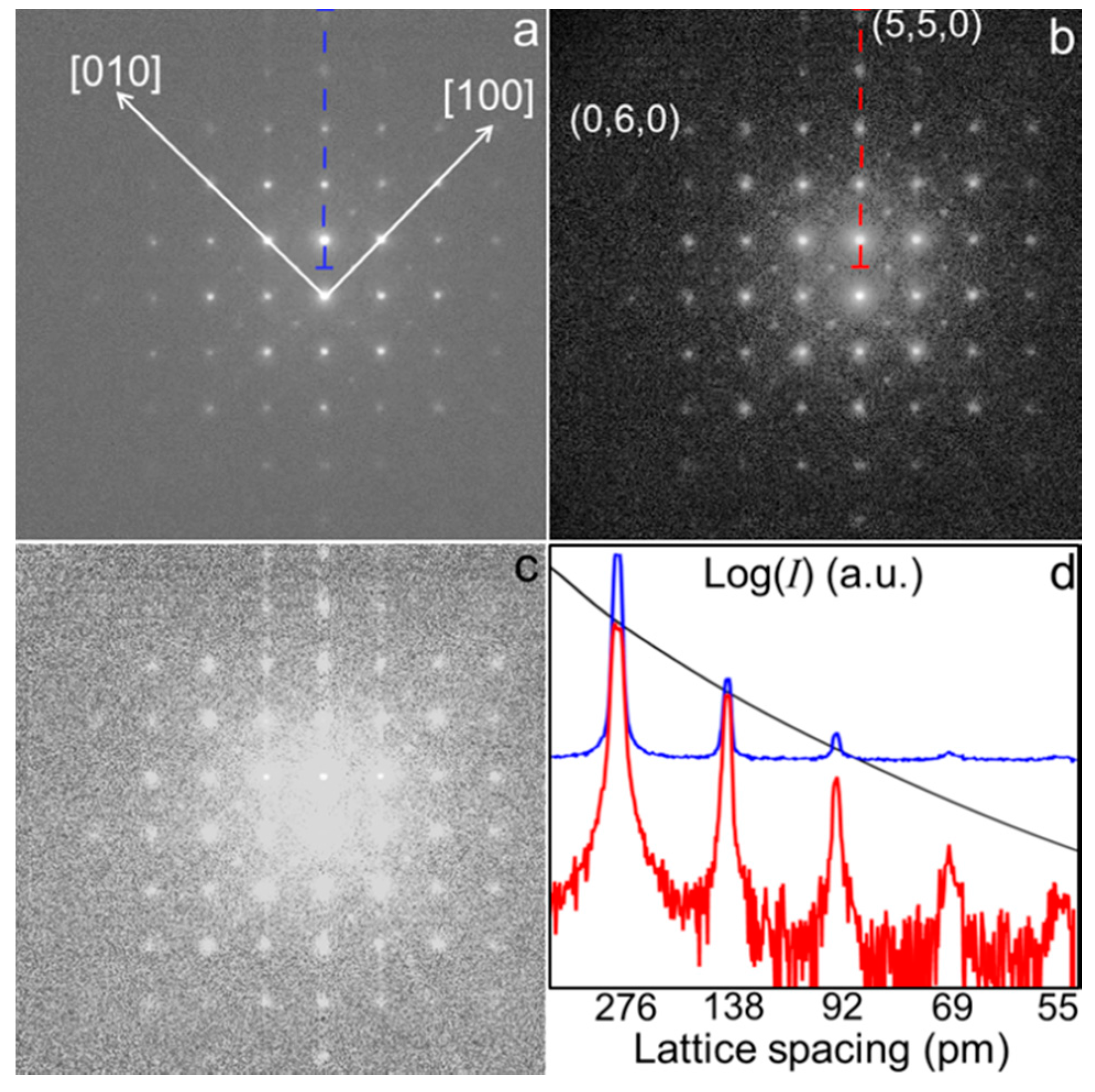
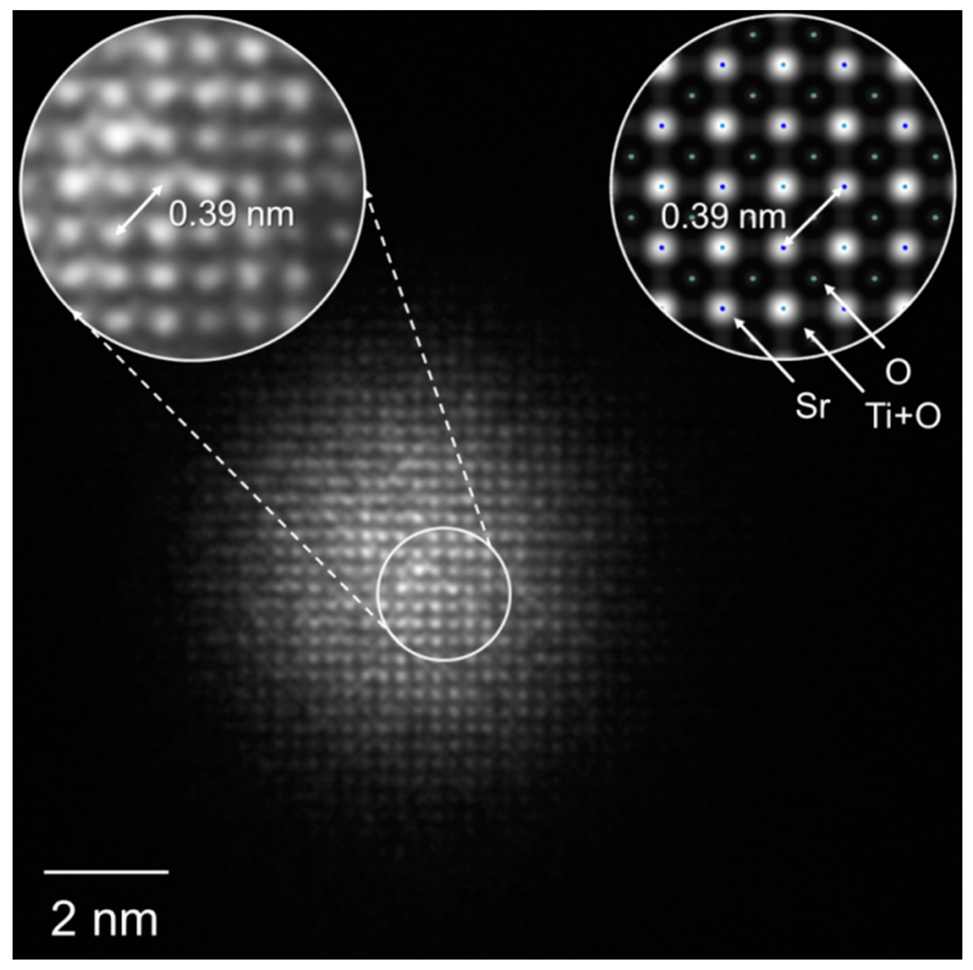
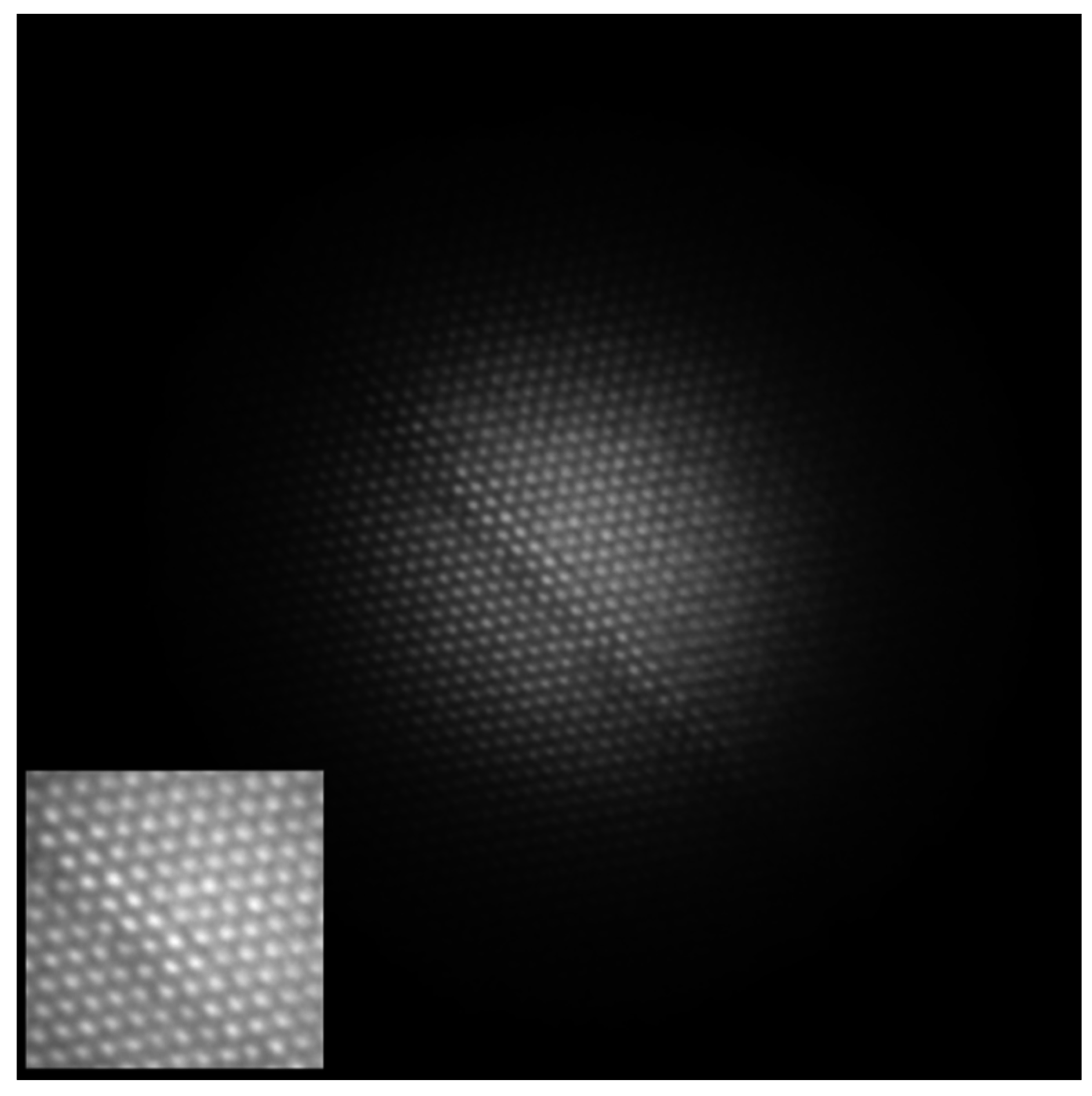
2.1. Electron Diffraction Experiments with Nano-Sized Coherent Illumination

The experiments were performed by a JEOL-JEM-2010F-UHR (Jeol Ltd., Tokyo, Japan) operating at 200 kV equipped with a high-coherence Schottky-type cathode. The microscope has a resolution at optimum defocus in High resolution transmission electron microscopy (HRTEM) of 190 pm [7]. The optical setup produces a parallel electron nano-beam, which defines the confined spatial support of the scattering function, illuminating only a nano-metric region of the analyzed specimens. Let O be the nano-sized scattering area plus the non-illuminated surrounding area. To satisfy the Nyquist-Shannon theorem the nano-sized beam, i.e. the so-called spatial support S, has to be less than 50% of O [16]. The cathode emission condition and the electron optical illumination system have been set up to maximize the probe coherence on the smallest achievable illuminated area [16]. Current density lower than 0.1 pA/cm2 and low acquisition times enable the nano-diffraction pattern to be acquired, on the 1024 × 1024 charge-coupled-device (CCD) camera, without the beam stopper used to eliminate the direct beam. Thus all the diffracted intensities, including the zero-order beam, are measured in the nano-diffraction pattern.
The illumination area used for the experiments on a specimen of SrTiO3 in [100] zone axis is shown in the HRTEM image in Figure 1. The illuminated area in the direct space corresponds to a S/O ratio of about 22% and hence the oversampling conditions are well satisfied. It is worth noting that the spots of higher intensity in the HRTEM image describe a square lattice corresponding to the projected potential of the atomic columns of Ti+O and Sr (Figure 1). The relevant HRTEM image simulation for specimen thickness of 25.0 nm and underfocus of 41.3 nm, was calculated in the Bloch-waves approach by considering 100 excited beams [1]. The dots in the simulated image in the right inset of Figure 1 indicate the true positions of the projected atomic structure used in the calculation. Hence, a comparison of the simulation with the HRTEM shows that the atomic columns containing only oxygen are not visible in the experimental image.

2.2. Intensity Rescaling of the Nano-Diffraction Pattern

We found that quantitative structural atomic information can be extracted from the nano-ED pattern acquired from the area illuminated in Figure 1, provided that proper constraints are used. If the electron diffraction pattern were kinematical it would be straightforward to derive the projected potential [1]. Unfortunately the kinematical approximation for electron diffraction is never completely satisfied. The presence of dynamical effects in real experiments makes in many cases a troublesome problem to derive quantitative data from the measure of the electron diffraction intensities. The goal would be to find a method to rescale properly the intensities of experimental diffraction patterns in order to compensate the eventual presence of dynamical effects. In Bragg diffraction, atoms belonging to the same unit-cell generate secondary waves whose phases are a function of their relative position. It is possible to compute an upper limit of the diffracted amplitude as a function of the scattering angle, adding the amplitudes of secondary waves generated by all the atoms within the unit-cell irrespective of their relative positions within the cell. This enables the estimation of the maximum scattering amplitude of the structure Fmax(s) = Σifi(s), which is the sum of the scattering factors fi(s) of the atoms in the crystal unit cell. Any interference between waves scattered by different unit cells (Bragg peaks) will be characterized by an intensity lower or equal to |Fmax(s)|2. To evaluate Fmax(s) we need to know the atoms contained in the unit cell. An approximate estimation of the chemical composition of the specimen can be available either from the nominal composition of the sample or could be straightforwardly derived during the same experimental session by energy dispersive X-ray spectroscopy or electron energy loss spectroscopy. In our experiments we found that knowledge of the sample chemistry with an accuracy of about 10% is enough to guarantee the reliability of the results. Thus, the approximate knowledge of the chemical composition of the sample enables the estimation of Fmax(s). Atomic scattering factors are tabulated as a function of s = sinθ, where θ is the scattering angle. Thus, |Fmax(s)|2 decreases as a function of θ following well-established theoretical models [17]. Therefore, its value can be used as a mathematical constraint to rescale the intensity I of the experimental nano-diffraction with respect to the measured direct beam (Imax). It is important to underline that this mathematical constraint can be applied only if the nano-ED pattern contains the direct beam Imax.
Let’s define the constraint: sup{I(s)} = |Fmax(s)|2/|Fmax(0)|2 ≤ 1. The condition I(s)/Imax ≤ sup{I(s)} should be satisfied for each scattering vector modulus s, measured in the nano-diffraction. The average intensities Ibk(s), corresponding to the larger s values in the experimental diffraction pattern out of the Bragg peaks, are subtracted iteratively to the whole pattern until Ibk(s)/Imax ≤ sup{I(s)} is fulfilled. Unphysical negative values are constrained to zero. With this rescaling the measured direct beam becomes the zero-order reflection of the pattern. After the sup{I(s)}-rescaling some diffraction peaks may still not satisfy the condition I(s)/Imax ≤ sup{I(s)}, due to measurement errors, small tilt angles with respect to precise zone-axis and, mainly, because of residual dynamical scattering effects. Thus, diffracted intensities exceeding I(s)/Imax ≤ sup{I(s)} are further rescaled subtracting local mean intensity values. We found that this rescaling, in experimental cases with dynamical effects typical of specimen thicknesses up to a few tens of nm, as usual in TEM experiments, can enable the correct retrieval of atomic structural information from the experimental nano-diffraction patterns. In Appendix A we have reported some theoretical considerations about the proposed approach, discussing also its limits of applicability.
Figure 2 shows the results of the intensity-rescaling on SrTiO3 (100) ED-pattern. Figure 2a shows the raw nano-diffraction and Figure 2b the result after the rescaling, calculating sup{I(s)} by the Doyle and Turner atomic scattering factor model [17], according to the nominal composition of the specimen. Figure 2c shows the difference between patterns of Figure 2a,b. Figure 2d shows a comparison, in a logarithmic scale, between the line profiles of the patterns in Figure 2a,b extracted from the scans highlighted in Figure 2, blue and red in (a) and (b), respectively. In Figure 2d also the corresponding profile of sup{I(s)} is plotted (black curve). The diffraction spot with the highest Miller’s index along the scans is the (5,5,0), which corresponds to a lattice spacing of 55 pm. Also the (0,6,0) reflection has been highlighted, corresponding to a lattice spacing of 65 pm, since the experimental pattern contains all Friedel’s pairs up to this resolution.

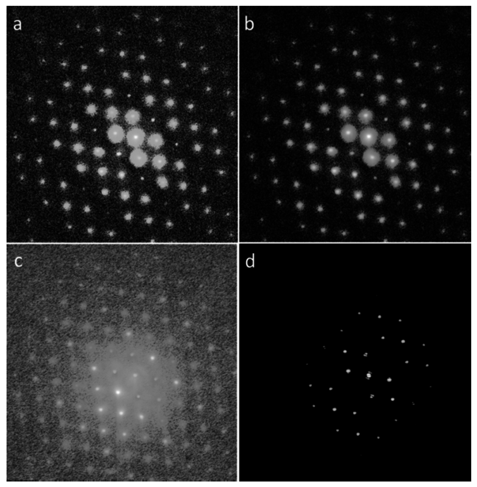
2.3. Auto-Correlation Function

The inverse FT of the rescaled diffraction pattern contains information on the scattering potentials. In X-ray crystallography the inverse FT of the measured diffracted intensities is the Patterson function, which can be deconvolved to extract structural information [18]. In fact, in X-ray crystallography the Patterson function is an aliased version of the unit cell electron density autocorrelation function, because its linear dimensions are double with respect to the lattice cell parameters. In the case of nano-diffractions taken from nano-regions of an extended crystalline structure, if the Nyquist-Shannon sampling is satisfied, the square modulus of the inverse FT of the measured intensities is not aliased [16]. Indeed, the zero scattering region around the illuminated nano-area of the sample enables one to obtain a non-aliased projected atomic potential auto-correlation function C(r) directly by the square modulus of an inverse FT of the sup{I(s)}-rescaled nano-diffraction pattern, where r is the position vector in the direct space. This auto-correlation function could be deconvolved, likewise Patterson functions, leading to non-aliased maps of the projected atomic potential. The procedure has been described in the Methods section.
Moreover, the atomic potential V(r) is a complex function and the diffused electron wave in weak phase-object approximation is related to the potential by: ψ(r) ≅ 1 + iπλΦ(r), where Φ(r) = 2meV(r)/h2 [1]. Here, m, e, h and i, are the electron mass, charge, Plank’s constant and imaginary unit, respectively. The diffracted intensity I(s) can be approximated as I(s)∝(πλ)2|F(s)|2, where F(s) is the structure factor corresponding to the complex scattering potential Φ(r). The auto-correlation function C(r), obtained by the inverse FT of the measured nano-diffraction pattern I(s), is a complex Hermitian function: C(−r) = C*(r). It is proportional to Φ(r) ⊗ Φ*(−r), where “⊗” denotes the convolution operator and “*” denotes the complex conjugate. It is given by:
C ( r ) = e i 2 π s r I ( s ) d s e i 2 π s r I c s ( s ) d s + e i 2 π s r Δ I ( s ) d s = C c s ( r ) + i sin ( 2 π s r ) Δ I ( s ) d s .
Here, the diffracted intensity has been divided into the symmetric Ics(s) and anti-symmetric ΔI(s) contribution. From Equation (1) the imaginary part of C(r) depends only on the non-centrosymmetric component of the diffraction pattern, as Ccs(r) is real and positive. A first contribution to the asymmetry of the electron diffraction pattern is due to misalignment of the crystal with respect to zone axes. An essential part of the non-centrosymmetric component is due to dynamical scattering [19], which is directly related to the thickness of the specimen (see Appendix A). Another contribution to the non-centrosymmetric part of the electron nano-diffraction pattern is due to absorption and derives from inelastic interactions such as phonon and plasmon scattering and single electron excitations from inner atoms [20,21]. For thin specimens this last effect contributes very little to the complex part of the object scattering function, which is only a few percent of the real part [6,7]. Moreover, the cross section from phonon scattering is sharply peaked at the atom cores and the corresponding absorption effects can be described by introducing a complex potential where the imaginary part ΦI(r) is proportional to the real part ΦR(r) [21,22]. Thus, Φ(r) = ΦR(r) + iΦI(r) ≅ ΦR(r) + iαΦR(r), with α very small, of the order of 0.01–0.05 for many atomic species [20]. Therefore, for centrosymmetric projected potentials almost all the asymmetry of the electron diffraction pattern for thin specimens can be ascribed to misalignment of the crystal with respect to zone axes, and the phase of the complex scattering function Φ(r) would have no further information about the sample’s atomic structure not already contained into its modulus. Therefore, all structural information will be contained in Ccs(r) ≅ ΦR(r) ⊗ ΦR(r) × (1 + α2). Instead, in the case of thin samples and non-centrosymmetric projected potentials, in conditions of a nano-sized illumination, ΔI(s) could give direct information about the anti-symmetric part of ΦR(r), whereas Ics(s) is related to both the symmetric and anti-symmetric parts of the potential (see Appendix A).

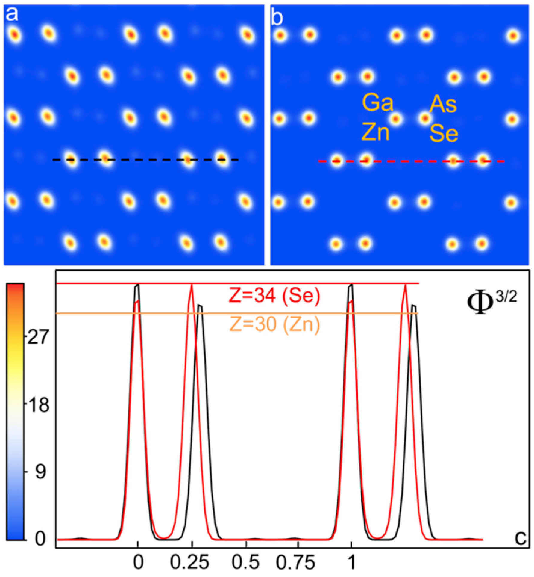
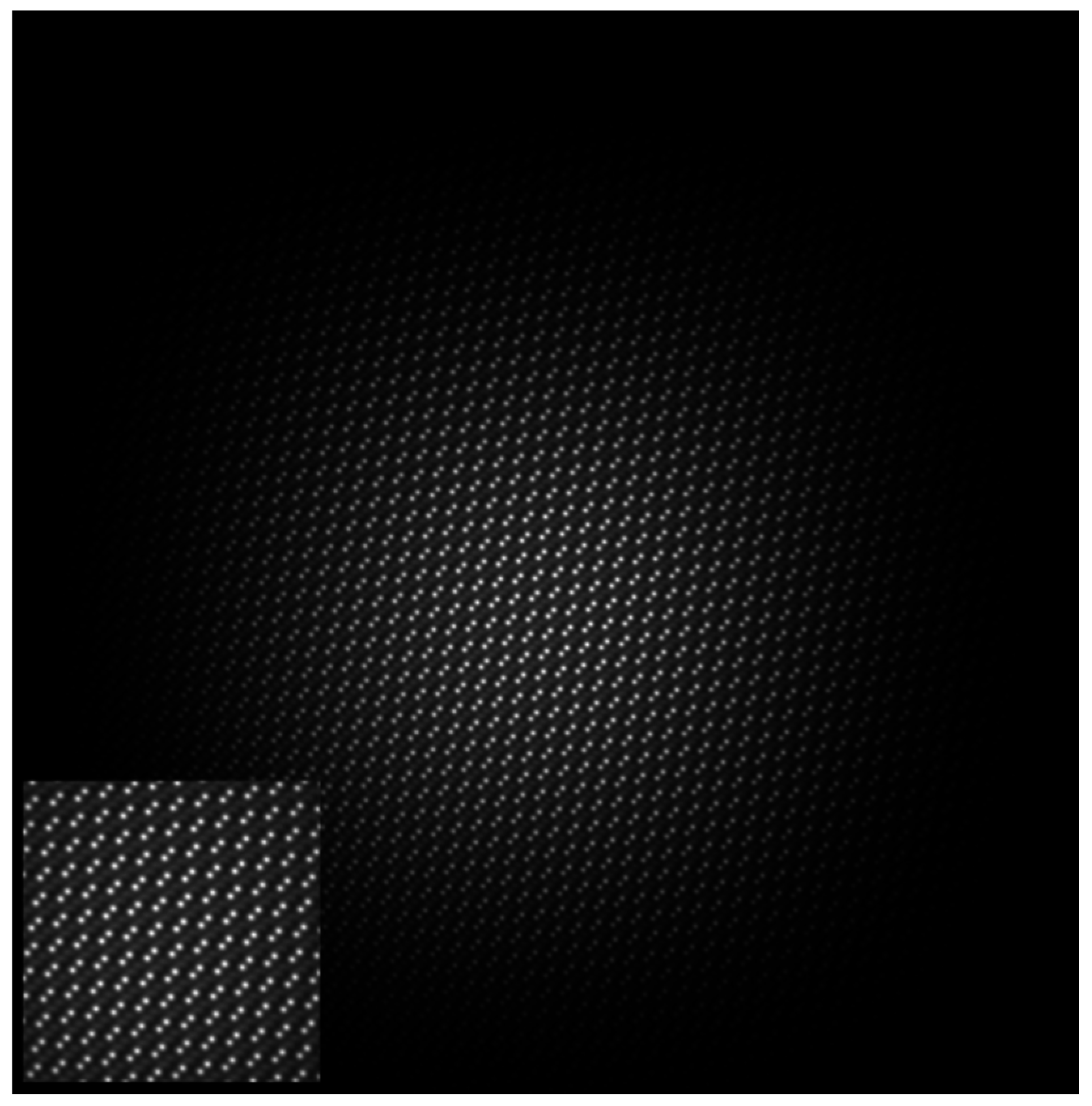
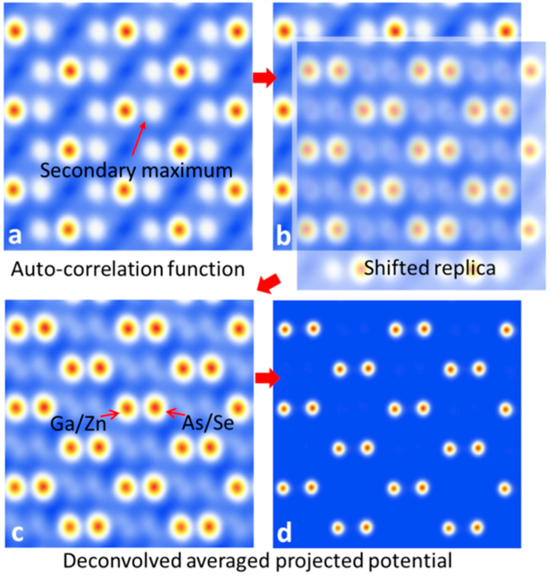
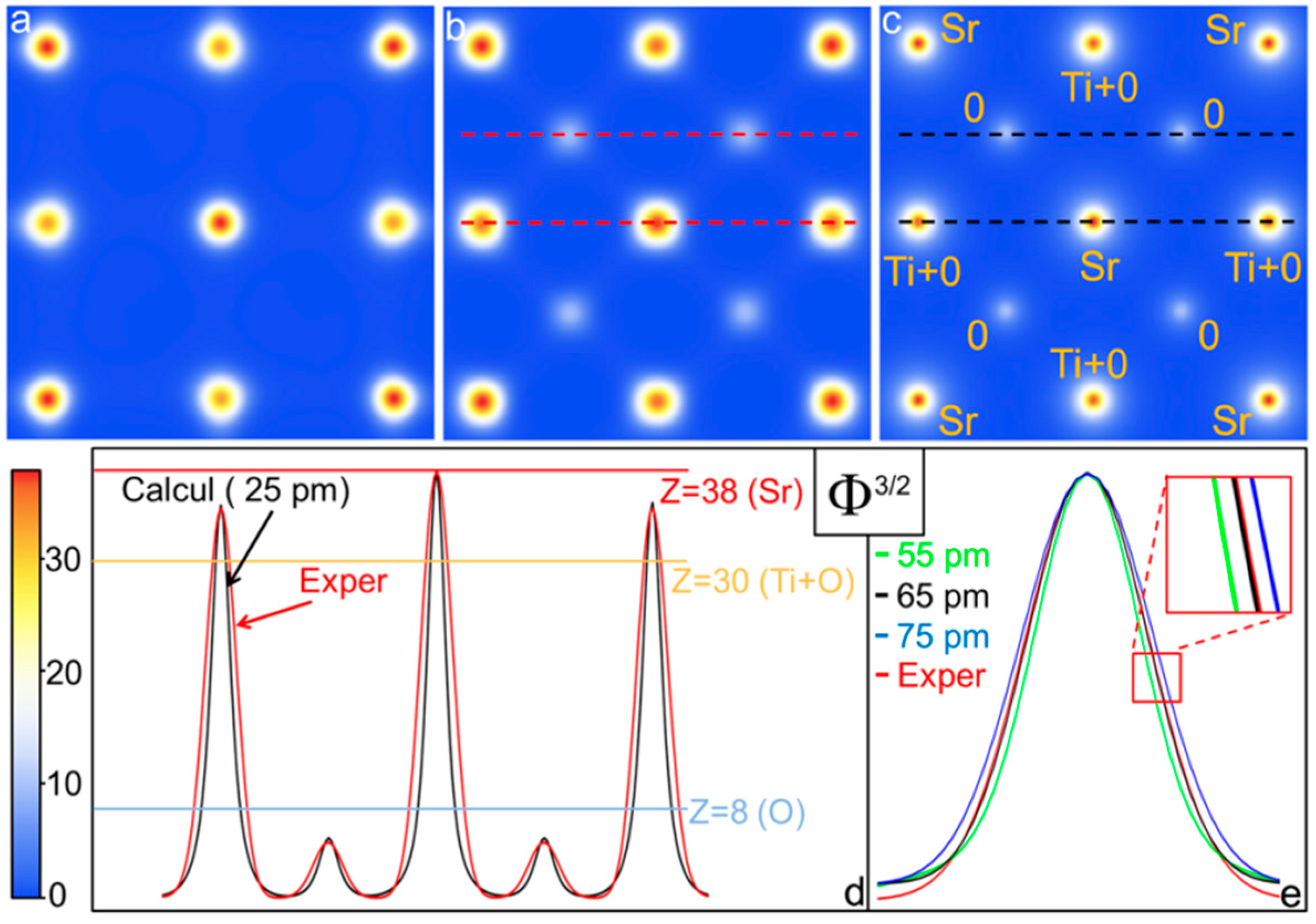
2.4. Deconvolution of C(R): Centrosymmetric Case

Since the [100] zone-axis projected atomic potential of the SrTiO3 is centrosymmetric, to simplify the notation, in the following let Φ(r) be its real part ΦR(r) and C(r) be its centrosymmetric part Ccs(r). The auto-correlation deconvolution of the real part of the nano-diffraction pattern can give the correct positions of the atomic species that contribute to the projected atomic potential, but it is proportional to Φ(r) ⊗ Φ(–r). Assuming that the shape of the atomic potential can be approximated with Gaussian functions, the width of the Φ(r) ⊗ Φ(–r) will be about 21/2 that of Φ(r). Moreover, projected atomic potential Φ is approximately proportional to Z2/3, with Z the atomic number [23] and C(r) is proportional to Z4/3. To obtain the correct relative scale between the values of the projected potential peaks belonging to different atomic columns, the square root C(r)1/2 has to be computed, whose width is 21/2 of C(r). Thus, to obtain the correct width of the peaks in the projected atomic potential map, namely Cdec(r), it is necessary to deconvolve C(r)1/2 peaks to about one half of their initial width, obtained by 1/21/2 × 1/21/2.
Figure 3a shows the result of Cdec,raw(r) for the raw experimental nano-diffraction of Figure 2a, whereas Figure 3b shows the result of Cdec,resc(r) for the rescaled nano-diffraction of Figure 2b. Figure 3c shows the SrTiO3 potential in [100] zone-axis projection calculated by the simulation program JEMS (Java Electron Microscopy Simulations) [24]. Figure 3d shows the sum of two scans highlighted with red dashed lines in Figure 3b (red curve) and the sum of two scans highlighted with black dashed lines in Figure 3c (black curve) to compare the SrTiO3 simulated projected atomic potential with that retrieved from the deconvolution of the experimental rescaled diffraction pattern. Moreover, in Figure 3d the calculated and experimental potentials Φ have been normalized with respect to their maxima, elevated to power 3/2 and multiplied by Z = 38 (Sr) to compare the final result directly with the average atomic number of the atoms contributing to the different columns of the projected atomic potential [23]. Figure 3e shows a zoom of the Sr peak to compare its experimental width, obtained by the deconvolution (red curve), with projected atomic potential values simulated at different spatial resolutions, from 55 pm to 75 pm. Debye-Waller factor values at room temperature are taken from JEMS [24]. Note that the deconvolution of the auto-correlation raw data (Figure 3a) does not show the correct structure for SrTiO3 as the oxygen atomic columns are missing. Furthermore, the maximum of the Ti+O projected potential is 16% lower than the calculated value. This is expected mainly because the dynamical effects mix the intensity of the diffracted waves [1].
Conversely, after sup{I(s)}-rescaling the deconvolved auto-correlation shows the correct average [100]-projected SrTiO3 atomic structure, including the oxygen columns. Figure 3d shows that the result is not only qualitatively in agreement with the calculated SrTiO3 atomic potential, but also quantitatively. For Ti+O and O columns the maxima of the experimental projected potentials are both about 4% smaller than calculated values. This is, in fact, a good quantitative result considering that the crystal potential calculations performed by linear combination of atomic potentials are affected by an error of about 10% [25]. Moreover, as shown in Figure 3e, the peak width differences between experimental and calculated potentials are due to the finite spatial resolution corresponding to the finer spatial spacing recorded in the diffraction pattern. Indeed, the best agreement between experimental and calculated potentials is obtained for a spatial resolution of 65 pm. As shown in Figure 2b, all reflections with lattice spacing larger or equal to 65 pm have been measured, enabling the achievement of a spatial resolution for the retrieved averaged projected atomic potential of (65 ± 2) pm.
The thickness of the sample was (25 ± 2.5) nm. It has been evaluated by comparing the ratio of the diffracted intensities with the dynamical calculations as a function of the specimen thickness. The value of 25 nm implies a dynamical scattering not negligible. It is about 25% of the extinction distance [1] of the (110) reflection, the most intense reflection shown in the scan of Figure 2b. This is why we cannot see at all the oxygen atomic columns in the deconvolved auto-correlation function of the raw data (Figure 3a) and also why the visible experimental Ti+O projected atomic potentials are not in quantitative agreement with the calculated values. Conversely, we found that the projected atomic potential can be correctly retrieved after sup{I(s)}-rescaling of the nano-diffraction data demonstrating a successful recovery of the experimental data from the dynamical effects.

2.5. Deconvolution of C(R): Non-Centrosymmetric Case

Figure 4 shows a HRTEM image focused at the interface between GaAs/ZnSe. The features of the interface in the HRTEM image are shown magnified in the relevant inset. This experiment is the analogous one of that shown in Figure 1 but now the projected atomic potential is non-centrosymmetric, as the GaAs and the ZnSe have the structure of the sphalerite. Furthermore, the presence of the interface introduces a geometrical asymmetry that enables one to investigate further the peculiarities of this new approach also in the presence of extended defects breaking the crystal perfection. The heterostructure is made by a ZnSe epilayer grown by molecular beam epitaxy on a (001) GaAs substrate. TEM sample is prepared in [110] cross-sectional geometry. The details of the specimen growth and TEM sample preparation have been reported in a previous work [26].
The resolution of the HRTEM image in Figure 4 is 0.19 nm [26] and it is not enough to distinguish the cations and anions atomic columns spacing of 0.14 nm in this projection. The illuminated area and electro-optical conditions in Figure 4 are those in which the experimental diffraction pattern shown in Figure 5a was acquired according to the Nyquist’s sampling requirement. Figure 5b shows the diffraction pattern, obtained by performing the sup{I(s)}-rescaling. Figure 5c shows the difference between the measured raw pattern and that obtained after the sup{I(s)}-rescaling. Figure 5d shows the anti-symmetrical part of the rescaled diffraction pattern, which can be directly related to the non-centrosymmetric part of the atomic projected potential, as shown in Appendix A.
In Figure 6 we show the deconvolution of the autocorrelation functions for the raw diffraction data (Figure 6a) and after the sup{I(s)}-rescaling (Figure 6b), taking into account the contribution of non-centrosymmetric part ΔI (see Appendix A).
As it can be evinced by the scans reported in Figure 6c the restored intensities lead to the average correct potential (red curve), with the correct relative positions of the two sub-lattices, at a fractional coordinate distance of 0.25 in the [110] projection. Moreover, also the relative intensities of the cation Ga/Zn columns (average Z of 30.5), with respect to the anion As/Se columns (average Z of 33.5) are correctly displayed from a quantitative point of view. Conversely, the projected average potential obtained by the measured intensities not restored (black curve in Figure 6c) is characterized by a wrong relative position of the two sphalerite sub-lattices, which appears separated in fractional coordinates of 0.29 in the [110] projection. This finding can be considered as a direct consequence of the dynamical scattering, which affects the measured diffraction pattern, and it confirms what already was obtained in a previous work in the study of the [211]-oriented Si samples [9,16].
Figure 7 shows the whole projected potential derived from the rescaled diffraction pattern shown in Figure 5b. It can be compared with the HRTEM image shown in Figure 4. It should be noted how in the map the cation-anion projected atomic potential spaced by 0.14 nm can now be distinguished whereas this was convoluted in the relevant HRTEM image due to the poorer resolution limited by the spherical aberration of the objective lens. The figure also points to how the information on the interface position is now missing, as the atomic potentials are averaged over the whole illuminated area. Hence local geometrical information is absent. In the same way, any other structural defect or non-periodic structural/chemical feature would not be visible. To retrieve local structural information about the interface and any other defect, an EDI phasing procedure is needed [7].
For a theoretical insight on the proposed approach, to restore nano-diffraction data affected by dynamical scattering for typical TEM experiments on standard specimen thicknesses up to few tens of nm, see Appendix A.

3. Methods

Deconvolution of the Autocorrelation Function

In this section we have briefly schematized some details of the method used to deconvolve the auto-correlation function of the projected atomic potentials. In Figure 8, as example, we have shown the result obtained in the particular case of the rescaled pattern shown in Figure 5b. Deconvolution of a non-aliased auto-correlation function C(r) can be performed in two ways: (1) multiplying C(r) times its translated replica on a secondary maximum rM, i.e., times C(rrM); (2) finding the minimum between C(r) and C(rrM) [18]. Moreover, in the presence of crystallographic symmetries it is possible to impose symmetry operators Si to C(r), for I = 1, m independent symmetries, obtaining m C(rSir) [18]. In this case the deconvolution can be obtained either multiplying C(rrM) times all the m independent of C(rSir) or finding the minimum between C(rrM) and all the m independent of C(rSir).
Figure 8a shows the auto-correlation function C(r) obtained by the inverse FT of the sup{I(s)}-rescaled diffraction pattern corresponding to the example of the ZnSe/GaAs heterostructure, oriented in a [110] zone axis, discussed in the previous section. Figure 8b shows the shifted replica of the auto-correlation function C(r-rM) centered on a secondary maximum rM. Figure 8c shows the product of C(r) and C(r-rM). Since in the illuminated area atomic columns belonging to both the substrate and to the epilayer are present, as schematically indicated in Figure 8c, we find on the cations and anions atomic columns the contributions of both materials constituting the heterostructure. Thus, the projection of one sub-lattice will give the average atomic potential corresponding to the Ga (Z = 31) and Zn (Z = 30) atomic columns. The other will give the average atomic potential corresponding to the As (Z = 33) and Se (Z = 34) atomic columns. Figure 8d shows the final projected atomic potential obtained deconvolving the increased width of the atomic columns due to the auto-correlation, as discussed in the previous section. This goal can be accomplished by deriving the Point Spread Function (PSF) directly from the normalized C(r) main peak. Hence, the next step is to deconvolve the square root of C(r) (see Section 2), by applying a Lucy-Richardson (LR) deconvolution approach, until about one half of its initial peak width is reached [27]. When the projected atomic potential is non-centrosymmetric, as in the example shown in Figure 8, the anti-symmetrical part ΦA(r) can be directly estimated by the inverse FT of ΔI and added to the symmetrical part determined by the deconvolution of the inverse FT of the centrosymmetric component ICS of the diffraction pattern (see Appendix A).

4. Conclusions

We have presented experimental results and data analysis based on: (i) preparation of a coherent nano-beam of 200 kV electrons and measurement of a complete (without beam-stopper) coherent diffraction pattern from a nano-region of extended samples, satisfying the Nyquist-Shannon sampling requirement; (ii) scaling of the measured intensities by imposing a mathematical constraint related to the maximum scattering amplitude that can be associated to the structure; (iii) deconvolution of the auto-correlation function obtained by the modulus of inverse FT of the rescaled nano-diffraction pattern to derive the average projected atomic potential. The results show a straightforward reconstruction for both centrosymmetric and non-centrosymmetric specimens in good quantitative agreement with the theoretical expectation. This is a new method for the study of matter at sub-atomic resolution that in many cases allows the overcoming of the limitations imposed by dynamical effects to quantitative structure analyses by electron diffraction. The method enables the measurement of the projected potential averaged on the illuminated nano-area, meaning that the presence of any eventual defect in this area is smeared over the whole average potential, slightly increasing the error in its determination. Nevertheless, the method gives quite readily the average potential on an area of few nm, without any need to retrieve phases, which in turn requires the knowledge of the support corresponding to the illumination beam. Moreover the proposed approach can be considered as a tool to restore diffraction data affected by dynamical effects in typical TEM experiments on standard specimen thicknesses up to a few tens of nm, making the pattern suitable for EDI phasing procedures capable of detecting local variations due to structural defects. Thus, the method makes also possible a wider application of EDI, partially relaxing the strong restrictions imposed on the thickness of the specimen by the dynamical nature of electron-matter interaction. It can be expected also that other crystallographic approaches based on electron diffraction could benefit from these findings.

Acknowledgments

The work was funded by PRIN 2012 NOXSS and Progetto premiale MIUR 2013 USCEF. Giorgio Rossi and Cinzia Giannini are acknowledged for critical reading of the manuscript and useful discussions.

Author Contributions

Elvio Carlino designed and performed the TEM experiments contributing also to the data reduction; Liberato De Caro, and Francesco Scattarella implemented the method into a computer program and processed the experimental TEM data; Liberato De Caro developed the theoretical background of the proposed method. Elvio Carlino, Liberato De Caro, and Francesco Scattarella discussed the results and wrote the paper.

Conflicts of Interest

The authors declare no conflict of interest.

Appendix A: Theory

In this appendix we present a general theoretical framework to understand the role and the limits of the proposed method to restore dynamical nano-diffraction data.

Appendix A1. Electron Wave Function for a Nano-Sized Illumination Beam

Structural information on samples is contained in the relevant diffraction patterns recorded at far field. The scattered intensity is:
I ( s ) = | ψ ( r ) exp [ i Φ ( r ) ] exp [ i 2 π s r ] d r | 2
where Φ(r) = 2meV(r)/h2, V(r) is the Coulomb atomic potential of the sample and ψ(r) the illuminating electron wave function. Here, m, e, h, and i, are the electron mass, charge, Planck constant and imaginary unit, respectively. In general, the illuminating electron wave function can be written as ψ(r) = A(r)exp[iϕ(r)], where A(r) is the wave amplitude and ϕ(r) the phase. It can be expressed also as a wave packet superposition [5]:
ψ ( r ) = g ( s ) exp [ i π s 2 λ ( C s λ 2 2 s 2 + Δ f ) ] exp [ i 2 π s r ] d s
where Cs and Δf are the spherical aberration and the defocus of the electron objective lens, respectively. Here, g(s) is the wave amplitude with wave vector k = 2πs. The finite width of g(s), necessary to form a nano-sized illumination, limits the lateral coherence of the electron beam. In turn, this leads to a smaller field of view and a higher intensity in the center of the illuminated nano-region [5]. This is just what happens in experimental conditions for which an incident nano-sized beam has a maximum intensity at its center and assumes a decreasing amplitude profile as a function of r, described by the function A(r) = |ψ(r)|, going to zero within few nm from its maximum (see, for example, Figure 1).

Appendix A2. Transverse Coherence Length

In a real TEM nano-diffraction experiment the incident electron wave has an angular divergence γ, representing a bundle of plane waves incident on the object. To estimate the upper limit of the beam angular spread γ, considering Δr~5 nm, i.e., of the order of half size of the illuminated area in Figure 1, from the uncertainty principle we obtain ΔkΔr = 2πγΔr/λ~1. As the wavelength of 200 keV electrons is λ ≅ 2.5 pm, γ~λ/(2πΔr)~80 μrad. Here, k = 2πs, so the finite value of the angular divergence leads to a finite transverse coherence length, given by
Lc~λ/(2γ).
For γ~80 μrad we obtain Lc~15 nm. Therefore, choosing a proper experimental setup, an illuminated area of 2Δr~10 nm can be, in principle, coherently illuminated.

Appendix A3. Compensation of Non-Linear Phase Shifts

The phase of the illuminating wave depends on the microscope electro-optical parameters (Equation (A2)). Indeed, the non-linear information transmission of the diffracted beams, described by the phase factor of Equation (A2), is mostly determined by the design of the objective lens, in which the only tuning parameter in equipment not Cs corrected is the defocus Δf. In weak-phase approximation the nonlinear phase transformation of the objective lens does not affect the experimental diffraction pattern [1], since the transfer function of Equation (A2) is described by a phase-factor with unitary modulus. Conversely, the corresponding image is strongly affected by the non-linear phase shift introduced by the objective lens. This is why in HRTEM experiments the defocus is tuned to obtain a slowly varying phase factor in a suitable range of frequencies to produce an experimental result not strongly dependent on the rapid oscillations of the phase [1] (see Figure 1).
π s 2 λ ( C s λ 2 2 s 2 + Δ f ) π 2
In general, in case of nano-beam illumination, the nonlinear phase transformation of the objective lens could, in principle, affects also the diffraction pattern yielding a complex illumination function. Nevertheless, choosing illuminating conditions to make the non-linear phase shift almost constant for each s, from Equation (A2) it follows that ϕ(r) would be slowly variable over the spatial region where A(r) ≠ 0. Under this condition the illuminating function can be approximated by ψ(r) ≅ A(r), neglecting the low spatial variability of phase ϕ(r) as a function of r.

Appendix A4. Dynamical Effects on the Non-Centrosymmetry of the Diffraction Pattern

Denoting with FT−1[I] the inverse FT of Equation (A1), ψ(r) ≅ A(r) and applying the product approximation to describe the phase shift introduced by the sample on the incident wave [28] we obtain
C ( r ) = FT 1 [ I ( s ) ] = { A ( r ) exp [ i Φ ( r ) ] } { A ( r ) exp [ i Φ * ( r ) ] } .
To simplify the notation, in the following we will suppress the explicit dependence on s and r. Here “⊗” denotes the convolution product and “*” the complex conjugate. C is the auto-correlation of the complex function A exp(iΦ).
As already stated, Φ(r) = ΦR(r) + iΦI(r) ≅ ΦR(r) + iαΦR(r) = (1 + iα)ΦR(r), where ΦR(r) is proportional to the Coulomb projected atomic potential and α of the order of 0.01–0.05 for many atomic species [20]. Structures with atoms of different species can be described by α = α(r), with α(r) << 1. Therefore, Equation (A5) can be rewritten as:
C = FT 1 [ I ] = [ A exp ( i Φ R ) exp ( α Φ R ) ] [ A exp ( i Φ R ) exp ( α Φ R ) ] .
The term exp(−αΦR) describes the absorption. Equation (A6) gives the dynamical intensity scattered by the sample for a nano-sized illuminating beam with amplitude A(r). Let us note that the right side of Equation (A6) is real if ΦR(r) is centrosymmetric [19] and A(r) = A(−r). In this case, rewriting the complex exponential functions in terms of trigonometric functions it gives:
C = FT 1 [ I ] = [ A cos ( Φ R ) exp ( α Φ R ) ] [ A cos ( Φ R ) exp ( α Φ R ) ] + [ A sin ( Φ R ) exp ( α Φ R ) ] [ A sin ( Φ R ) exp ( α Φ R ) ] .
If ΦR(r) is centrosymmetric, a straightforward calculus shows that complex terms cancel each other and, as already stated, any non-centrosymmetry in the measured diffracted pattern can be almost fully ascribed to mis-tilts of the crystalline sample with respect to the precise zone axis orientation. However, it should be noted that for nano-sized illuminations another possible cause of non-centrosymmetry of the diffraction pattern obtained by a centrosymmetric projected potential could be ascribed to an asymmetric nano-beam illumination, i.e., A(r) ≠ A(–r).
From Equation (A5) it follows that the diffracted wave is the sum of the FT of a cosine and a sine terms. For a non-centrosymmetric projected potential we can rewrite the cosine and sine terms as the sum of symmetric and anti-symmetric components [19]:
cos [ Φ R ( r ) ] = 1 2 { cos [ Φ R ( r ) ] + cos [ Φ R ( r ) ] } + 1 2 { cos [ Φ R ( r ) ] cos [ Φ R ( r ) ] } sin [ Φ R ( r ) ] = 1 2 { sin [ Φ R ( r ) ] + sin [ Φ R ( r ) ] } + 1 2 { sin [ Φ R ( r ) ] sin [ Φ R ( r ) ] } .
Denoting the FT of the above components as Ccos, iAcos and Csin, iAsin, respectively, it results:
I ( ± s ) = | A ˜ FT [ exp ( α Φ R ) ] [ C cos ± i A cos + i ( C sin ± i A sin ) ] | 2 = | A ˜ FT [ exp ( α Φ R ) ] [ C cos A sin + i ( C sin ± A cos ) ] | 2 .
Here, the symbol “~” denotes the FT. Thus, I(s) ≠ I(−s) and the diffraction pattern would be non-centrosymmetric, also for a symmetric illumination function A(r) = A(–r). For a centrosymmetric ΦR(r) = ΦR(–r) the anti-symmetric components Acos and Asin would be negligible and, if A(r) = A(–r), from Equation. (A9) readily it would follow that I(s) = I(–s), as previously stated. Conversely, for a non-centrosymmetric projected potential even small dynamical effects would produce breaking of Friedel’s pair symmetry, independently of any mis-tilt of the specimen with respect to the precise zone axis.

Appendix A5. Weak Phase Approximation

If ΦR << 1, from Equation (A9) the so-called Weak Phase Approximation (WPA) is obtained expanding in series the trigonometric functions up to the first order in ΦR and neglecting the absorption terms. Under WPA the diffracted intensity is readily derived by the FT of the following Equation:
C W P A = FT 1 [ I W P A ] = A A + ( A Φ R ) ( A Φ R ) + O ( Φ R 2 ) ,
leading to:
I W P A = | A ˜ | 2 + | A ˜ Φ ˜ R | 2 .
The first term in the right side of Equation (A11) gives the direct beam, which is the FT of the autocorrelation function of the incident nano-beam amplitude A. Whereas the last term of Equation (A11) gives the WPA diffracted pattern, which is the FT of the auto-correlation function of the projected atomic potential ΦR times the incident nano-beam amplitude A. Thus, the widths of Bragg peaks will be directly related to the size and shape of the illumination nano-beam.

Appendix A6. Second-Order Dynamical Perturbation to the Weak Phase-Approximation

In TEM the condition ΦR << 1 is violated even for few unit cells’ sample thickness. A dynamical scattering factor fdyn can be formally defined as [28]
FT 1 [ i f k i n ] = exp ( i Φ ) 1 ,
Whereas the kinematical scattering factor fkin is directly related to the WPA projected potential:
FT 1 [ i f k i n ] = F T 1 [ i f W P A ] = i Φ .
Thus, the dynamical contribution to scattering for a nano-size illumination beam will be given by:
FT 1 [ I I k i n ] = [ A ( exp ( i Φ R ) exp ( α Φ R ) 1 ) ] [ A ( exp ( i Φ R ) exp ( α Φ R ) 1 ) ] ( A Φ R ) ( A Φ R ) .
Expanding in series Equation (A14) up to the second-order, and neglecting small absorption terms, it leads to:
FT 1 [ I I k i n ] = [ A Φ R 2 / 2 ] [ A Φ R 2 / 2 ] + O ( Φ R 3 ) .
Hence:
I | A ˜ Φ ˜ R Φ ˜ R | 2 / 4 + I W P A > I W P A .
Equation (A16) indicates that the phase of the dynamical scattering factors [28] takes an active part in the scattering process since in the convolutions there is Φ ˜ R with its phase. Thus, in general, fdyn is not a real quantity. This finding will cause destructive interferences for some Bragg reflection amplitudes and constructive for others, through multiple scattering, described by the convolution operation inside the square modulus. Nevertheless, the square modulus of the second order dynamical term will be added to the kinematical contribution obtainable in a WPA. Therefore, if any of the Bragg reflections would be affected by dynamical scattering, the corresponding diffracted intensities would increase for the second-order dynamical contribution. By considering higher orders in the power expansion of the trigonometric functions some terms could give a negative contribution to the intensity of some Bragg reflections, but the overall result, for sample thickness smaller than half of the corresponding extinction distances, would be to increase the diffracted intensities, reducing the direct beam intensity.
This finding leads to the need to rescale diffracted intensities, as discussed in the paper, which are too large with respect to the maximum value of the scattering amplitude calculated from the a-priori approximate knowledge of the sample chemistry. This operation can be made by means of the two-dimensional radial function sup{I(s)}, as shown in the paper, depending on the scattering vector modulus s. Indeed, the approximate knowledge of the chemical composition of the sample enables one to estimate the maximum scattering amplitude of the structure Fmax(s) = Σifi(s), which is the sum of the scattering factors fi(s) of the atoms in the crystal unit cell assuming that all are adding constructively their scattered amplitudes. In this way the upper limit of any diffracted intensity, normalized to the incident beam intensity, can be readily evaluated. Therefore, the rescaling of the measured intensities by using the sup{I(s)} = |Fmax(s)|2/|Fmax(0)|2 constraint partially corrects the effect of the dynamical scattering, reducing the effect of the dynamical contribution of Equation (A16) and of other higher order terms to the diffracted intensities. Obviously, this does not assure that the rescaled diffracted intensity is fully corrected by dynamical scattering, but our experimental tests show that this rescaling of intensities is sufficient to guarantee the quantitative determination of the projected atomic potential. Indeed, the deconvolution of the modulus of the FT of the rescaled diffraction pattern readily gives the correct projected atomic potential ΦR(r) averaged in the nano-region where A(r) ≠ 0. Our experimental tests indicate that for sample thickness larger than one third of the smaller extinction distance, the dynamical effects cannot be recovered by the proposed approach. Nevertheless the range of applicability of the method is very wide because, usually, in standard TEM experiments the thickness of the specimen does not exceed a few tens of nm.
As in any crystallographic approach, the interferences of all crystals unit cells inside the illuminated volume leads to a very accurate determination of the coordinates of the atomic species. However, in this way any information about any structural defect is averaged and, consequently, lost. This is why in the case of GaAs/ZnSe, discussed in Section 2, the recovered projected atomic potential does not show any clue of the interface visible in the relevant HRTEM. To obtain local variations of the projected atomic potential, to realize the true imaging of the illuminated nano-region of the sample and visualize eventual defects, an EDI phasing approach is necessary, but this is beyond the scope of this work.

Appendix A7. General Equations

All the above results stand on the assumption of a slowly spatial dependence of the phase ϕ(r) of the illuminating electron wave function ψ(r) = A(r)exp[iϕ(r)]. When the dependence of the phase ϕ(r) on the spatial position r cannot be neglected Equation (A5) has to be generalized as follow:
C = FT 1 [ I ] = { A exp [ i ϕ ] exp [ i Φ ] } { A exp [ i ϕ ] exp [ i Φ * ] } = [ A cos ( ϕ + Φ R ) exp ( α Φ R ) ] [ A cos ( ϕ + Φ R ) exp ( α Φ R ) ] + [ A sin ( ϕ + Φ R ) exp ( α Φ R ) ] [ A sin ( ϕ + Φ R ) exp ( α Φ R ) ] .
In this case the illuminating function (electron probe) has to be phased to disentangle phase information regarding the sample, i.e., ΦR(r), from the contribution of the incident wave, i.e., ϕ(r). Indeed, the diffraction pattern will be characterized by several interferences related to the probe. The deconvolution of the illumination phase wave from the contribution of the sample is needed, for example, in X-ray Fresnel diffraction Keyhole CDI [29], in ptychography [30,31] and in any case in which it is not possible to tune properly the optical conditions for the lenses in order to suitably compensate non-linear phase components of the illuminating wave function.

Appendix A8. Incoherent Source Approximation

However, it should be noted that in some cases Equation (A17) can be simplified by more general theoretical considerations. Let us assume that a diffraction pattern is collected in the Fraunhofer geometry, which requires that both source-object and object-detector distances are much larger than object and source sizes. In these conditions, the fully coherent diffraction pattern recorded in far field from the sample is:
I c o h ( s ) | ψ ( r 1 ) ψ * ( r 2 ) exp [ i Φ ( r ) ] exp [ i Φ * ( r ) ] exp [ i 2 π s ( r 1 r 2 ) ] d r 1 d r 2 | .
If we are dealing with a beam of finite lateral size and non-null divergence, the coherence properties of the wave-field impinging onto the sample in the incoherent approximation can be described through the coherence function [32]:
ψ ( r 1 ) ψ * ( r 2 ) = J ( r 1 r 2 ) = J ( y ) .
Which is a function only of the relative distance y= r1 r2 between different points of the sample. From Equations (A18) and (A19) it results:
I ( s ) | exp [ i Φ ( r 1 ) ] exp [ i Φ * ( r 1 + y ) ] d r 1 J ( y ) exp ( i 2 π s y ) d y | = I c o h ( s ) | A ˜ ( s ) | 2 .
Here, | A ˜ ( s ) | 2 is the square modulus of the FT of J(y), directly related to the incident nano-beam shape and size. In these conditions the coherent dynamical diffracted intensity Icoh(s) is convoluted with the intensity profile of the incident beam. Equation (A20) implies that, in experimental situations similar to those treated in the present work, it is not necessary to know the incident illumination function in modulus and phase. This situation is substantially different from ptychography [30,31] or Fresnel X-ray Keyhole CDI [29]. Indeed, in some experiments it is sufficient to know only the intensity of the source probe. This finding is a consequence of the assumption (A19). It is valid only for monochromatic spatially incoherent sources, i.e., when the spatial coherence is developed through wave propagation and when we are dealing with the Fraunhofer diffraction geometry. This result is a direct consequence of the Van Cittert-Zernike theorem [32]. Indeed, in the far-field limit, the Van Cittert-Zernike theorem for an incoherent source relates the angular distribution of the wave-field impinging on the sample directly to the FT of the physical source square modulus amplitude. Equation (A20) can be assumed approximately valid also for Schottky TEM sources, used in the present work, because the spatial coherence of the electron waves emitted by these sources is reached by reducing their size on a small scale, but single electrons are emitted incoherently from each other by different regions of the sources. Under the condition given by Equation (A19) the inverse FT of I, given by Equation (A7), can be further simplified as follows:
C = FT 1 [ I ] = ( A A ) × [ cos ( Φ R ) exp ( α Φ R ) ] [ cos ( Φ R ) exp ( α Φ R ) ] + + ( A A ) × [ sin ( Φ R ) exp ( α Φ R ) ] [ sin ( Φ R ) exp ( α Φ R ) ] .
Equation (A21) implies that the beam profile can be considered as a multiplicative envelope that can be extracted by the convolution with the projected atomic potential ΦR(r). This is possible since A(r) is slowly variable as a function of r with respect to the ΦR(r) lattice periodicity and the phase ϕ(r) can be considered almost constant on the same spatial scale.

Appendix A9. Further Insight for the Kinematical Approximation

Non-centrosymmetric atomic projected potentials in the presence of dynamical scattering and absorption lead to a violation of the Friedel’s law, with I(s) ≠ I(–s). Thus, in general, the non-centrosymmetry implies that the auto-correlation function C(r) is a complex function. However, if the imaginary part of the potential is approximately proportional to the real part, for uniform illumination A(r) = const, in conditions of kinematical scattering and low absorbing samples, the imaginary part of C(r) is negligible also for non-centrosymmetric atomic projected potential. Indeed, let denote with ΦS(r) and ΦA(r) the symmetrical and anti-symmetrical part of the real component ΦR(r) of the projected potential, respectively:
Φ R ( r ) = Φ S ( r ) + Φ A ( r ) .
For kinematical scattering, i.e., in WPA conditions, we have
C k i n = { Φ S ( r ) + Φ A ( r ) + i α [ Φ S ( r ) + Φ A ( r ) ] } { Φ S ( r ) + Φ A ( r ) i α [ Φ S ( r ) + Φ A ( r ) ] } Φ S ( r ) Φ S ( r ) + Φ A ( r ) Φ A ( r ) + Φ A ( r ) Φ S ( r ) + Φ S ( r ) Φ A ( r ) .
In the above Equation the mixed terms ΦA(r)⊗ΦS(–r) and ΦS(r)⊗ΦA(–r) eliminates each other due to the even and odd parity of ΦS(r) and ΦA(r), respectively. Since α << 1, in Equation (A23) the term proportional to α2 has been neglected. Moreover, it is straightforward to verify that for the complex part, the term proportional to iα, is null. Therefore, the auto-correlation function will be real also for a non-centrosymmetric projected potential:
C k i n ( r ) = Φ S ( r ) Φ S ( r ) + Φ A ( r ) Φ A ( r ) = Φ S ( r ) Φ S ( r ) Φ A ( r ) Φ A ( r ) ,
from which
I k i n = FT [ C k i n ] = | Φ ˜ S | 2 + | Φ ˜ A | 2 = | Φ ˜ | 2 ,
since
FT [ Φ A ( r ) ] = i Φ ˜ A .
The situation changes for an illumination confined in a nano-region of the sample, as in the cases under study in this work. In this instance, inserting Equation (A22) into Equation (A9), for a symmetric illumination A(r) = A(–r) and a low absorbing sample, we obtain:
I k i n ( ± s ) = | A ˜ [ δ α ( Φ ˜ S + i Φ ˜ A ) ] [ δ Φ ˜ A + i Φ ˜ S ] | 2 .
Thus, even in absence of absorption, neglecting the term proportional to α, we obtain:
I k i n ( ± s ) = | A ˜ [ δ Φ ˜ A + i Φ ˜ S ] | 2 = | A ˜ A ˜ Φ ˜ A + i A ˜ Φ ˜ S | 2 = | A ˜ | 2 + | A ˜ Φ ˜ S | 2 + | A ˜ Φ ˜ A | 2 2 A ˜ ( A ˜ Φ ˜ A ) .
From Equation (A28) it follows
Δ I k i n ( s ) = I k i n ( s ) I k i n ( s ) = 4 A ˜ ( A ˜ Φ ˜ A ) ,
from which
FT 1 [ Δ I k i n ( s ) ] = 4 A ( A Φ A ) .
Thus, the anti-symmetric part of the diffraction pattern contains information regarding the anti-symmetric part of the projected potential. Therefore, if the rescaling of the measured intensities has allowed, at least partially, restoring of the diffraction data from dynamical effects, the deconvolution of the inverse FT of I could give the correct projected potential also for non-centrosymmetric cases. Indeed, in the incoherent source approximation, from Equations (A21) and (A30) the anti-symmetrical part ΦA(r) can be directly estimated by FT−1[I] and added to the symmetrical part determined by the inverse FT of the centrosymmetric component ICS of the diffraction pattern, as carried out in this work in the case of the specimen with the sphalerite structure discussed in Section 2.

References

  1. Reimer, L. Transmission Electron Microscopy: Physics of Image Formation and Microanalysis; Springer: Berlin/Heidelberg, Germany, 1984. [Google Scholar]
  2. Cowley, J.M. Electron Nanodiffraction. Microsc. Res. Tech. 1999, 46, 75–97. [Google Scholar] [CrossRef]
  3. Haider, M.; Rose, H.; Uhlemann, S.; Kabius, B.; Urban, K. Towards 0.1 nm resolution with the first spherically corrected transmission electron microscope. J. Electron. Microsc. 1998, 47, 395–405. [Google Scholar]
  4. Hawkes, P.W. Aberration correction past and present. Phil. Trans. R. Soc. A 2009, 367, 3637–3664. [Google Scholar] [CrossRef] [PubMed]
  5. Zuo, J.M.; Vartanyants, I.; Gao, M.; Zhang, M.R.; Nagahara, L.A. Atomic resolution imaging of a carbon nanotube from diffraction intensities. Science 2003, 300, 1419–1421. [Google Scholar] [CrossRef] [PubMed]
  6. Huang, W.J.; Zuo, J.M.; Jiang, B.; Kwon, K.W.; Shim, M. Sub-ångström-resolution diffractive imaging of single nanocrystals. Nat. Phys. 2009, 5, 129–133. [Google Scholar] [CrossRef]
  7. De Caro, L.; Carlino, E.; Caputo, G.; Cozzoli, P.D.; Giannini, C. Electron diffractive imaging of oxygen atoms in nanocrystals at sub-ångström resolution. Nat. Nanotech. 2010, 5, 360–365. [Google Scholar] [CrossRef] [PubMed]
  8. Zuo, J.M. Electron detection characteristics of a slow-scan CCD camera, imaging plates and film, and electron image restoration. Microscopy Res. Tech. 2000, 49, 245–268. [Google Scholar] [CrossRef]
  9. De Caro, L.; Carlino, E.; Siliqi, D.; Giannini, C. Coherent Diffractive Imaging: From Nanometric Down to Picometric Resolution. In Handbook of Coherent-Domain Optical Methods; Springer: Berlin, Germany, 2012. [Google Scholar]
  10. Sayre, D. Some implications of a theorem due to Shannon. Acta Cryst. 1952, 5, 843. [Google Scholar] [CrossRef]
  11. Miao, J.; Charalambous, P.; Kirz, J.; Sayre, D. Extending the methodology of X-ray crystallography to allow imaging of micrometre-sized non-crystalline specimens. Nature 1999, 400, 342–344. [Google Scholar] [CrossRef]
  12. Shannon, C.E. Communication in the presence of noise. Proc. Inst. Radio Eng. 1949, 37, 10–21. [Google Scholar] [CrossRef]
  13. Nyquist, H. Certain Topics in Telegraph Transmission Theory. Trans. AIEE 1928, 47, 617–644. [Google Scholar] [CrossRef]
  14. Zuo, J.M.; Zhang, J.; Huang, W.; Ran, K.; Jiang, B. Combining Real and Reciprocal Space Information for Aberration Free Coherent Electron Diffractive Imaging. Ultramicroscopy 2011, 111, 817–823. [Google Scholar] [CrossRef] [PubMed]
  15. Zou, X.; Hovmoeller, S.; Oleynikov, P. Electron Crystallography: Electron Microscopy and Electron Diffraction, 2nd ed.; International Union of Crystallography, Oxford Science Publications-Oxford University Press: Oxford, UK, 2012. [Google Scholar]
  16. De Caro, L.; Carlino, E.; Vittoria, A.F.; Siliqi, D.; Giannini, C. Keyhole electron diffractive imaging (KEDI). Acta Cryst. A 2012, 68, 687–702. [Google Scholar] [CrossRef] [PubMed]
  17. Doyle, P.A.; Turner, P.S. Relativistic Hartree-Fock X-ray and electron scattering factors. Acta Crys. A 1968, 24, 390–397. [Google Scholar] [CrossRef]
  18. Caliandro, R.; Carrozzini, B.; Cascarano, G.L.; De Caro, L.; Giacovazzo, C.; Siliqi, D. Advances in ab initio protein phasing by Patterson deconvolution techniques. J. Appl. Crys. 2007, 40, 883–890. [Google Scholar] [CrossRef]
  19. Liu, A.Y.; Lumpkin, G.R.; Petersen, T.C.; Etheridge, J.; Bourgeois, L. Interpretation of angular symmetries in electron nanodiffraction patterns from thin amorphous specimens. Acta Cryst. A 2015, 71, 473–482. [Google Scholar] [CrossRef] [PubMed]
  20. Radi, G. Complex lattice potentials in electron diffraction calculated for a number of crystals. Acta Cryst. A 1970, 26, 41–56. [Google Scholar] [CrossRef]
  21. Humphreys, C.J.; Hirsh, P.B. Absorption parameters in electron diffraction. Philos. Mag. 1968, 18, 115. [Google Scholar] [CrossRef]
  22. Wang, A.; Chen, F.R.; Van Aert, S.; Van Dyck, D. Direct structure inversion from exit waves: Part I: Theory and simulations. Ultramicroscopy 2010, 110, 527–534. [Google Scholar] [CrossRef]
  23. Vainshtein, B.K. Structure Analysis by Electron Diffraction; Pergamon Press Ltd.: London, UK, 1964; p. 208. [Google Scholar]
  24. J E M S-S A A S. Version 4.3931U2016. Available online: http://www.jems-saas.ch/ (accessed on 16 September 2016).
  25. Kirkland, E.J. Advanced Computing in Electron Microscopy; Plenum Press: New York, NY, USA, 1998. [Google Scholar]
  26. Colli, A.; Carlino, E.; Pelucchi, E.; Grillo, V.; Franciosi, A. Local interface composition and native stacking fault density in ZnSe /GaAs(001) heterostructures. J. Appl. Phys. 2004, 96, 2592–2602. [Google Scholar] [CrossRef]
  27. De Caro, L.; Altamura, D.; Vittoria, F.A.; Carbone, G.; Qiao, F.; Manna, L.; Giannini, C. A superbright X-ray laboratory micro-source empowered by a novel restoration algorithm. J. Appl. Cryst. 2012, 45, 1228–1235. [Google Scholar] [CrossRef]
  28. Peng, L.M. Quasi-dynamical electron diffraction-a kinematic type of expression for the dynamical diffracted-beam amplitudes. Acta Cryst. A 2000, 56, 511–518. [Google Scholar] [CrossRef]
  29. Abbey, B.; Nugent, K.A.; Williams, G.J.; Clark, J.N.; Peele, A.G.; Pfeifer, M.A.; de Jonge, M.; McNulty, I. Keyhole coherent diffractive imaging. Nat. Phys. 2008, 4, 394–398. [Google Scholar] [CrossRef]
  30. Rodenburg, J.M.; Faulkner, H.M.L. A phase retrieval algorithm for shifting illumination. Appl. Phys. Lett. 2004, 85, 4795–4797. [Google Scholar] [CrossRef]
  31. Rodenburg, J.M.; Hurst, A.C.; Cullis, A.G.; Dobson, B.R.; Pfeiffer, F.; Bunk, O.; David, C.; Jefimovs, K.; Johnson, I. Hard-X-Ray Lensless Imaging of Extended Objects. Phys. Rev. Lett. 2007, 98, 034801. [Google Scholar] [CrossRef] [PubMed]
  32. Born, M.; Wolf, E. Principles of Optics, VI edition; Pergamon Press plc: Oxford, UK, 1991; p. 510. [Google Scholar]
Figure 1. High resolution transmission electron microscopy (HRTEM) image of a nano-region of a SrTiO3 extended sample in [100] zone axis, with a zoom in the inset on the left. A simulation for underfocus 41.3 nm and specimen thickness of 25.0 nm is shown in the inset on the right. The dots in the simulation point to the structural positions of the SrTiO3 atomic species in this projection: Sr = Blue, Ti+O = pale blue, O = pale green.
Crystals 06 00141 g001
Figure 2. Intensity-rescaling on SrTiO3 (100) electron diffraction (ED)-pattern: (a) Raw experimental nano-diffraction pattern (logarithmic scale); (b) sup{I(s)} rescaled pattern; (c) difference between patterns shown in (a) and (b); (d) comparison in a logarithmic scale between the line profile along the dashed blue line in (a) (blue curve) and along the dashed red line in (b) (red curve) after rescaling. Black curve is the corresponding profile of sup{I(s)} × Imax constraint.
Crystals 06 00141 g002
Figure 3. Deconvolution of the projected atomic potential auto-correlation function C(r): (a) C(r) atomic projected potential obtained from raw experimental nano-diffraction data; (b) C(r) atomic projected potential obtained from rescaled nano-diffraction data; (c) SrTiO3 calculated projected atomic potential in [100] zone-axis; (d) red curve: sum of the two scans highlighted with the red dashed lines in Figure 3b; black curve: sum of the two scans highlighted with the black dashed lines in Figure 3c. In Figure 3d the experimental and calculated potentials Φ have been normalized to 1, plotted at a power of 3/2 and rescaled to have a maximum equal to Z = 38 (Sr); (e) zoom of the Sr peak to compare its experimental width (red curve), with projected potential values simulated at different spatial resolutions.
Crystals 06 00141 g003
Figure 4. HRTEM image in [110] zone axis focused at the GaAs/Znse interface. In the inset a magnified view of the HRTEM image contrast at the interface.
Crystals 06 00141 g004
Figure 5. Intensity-rescaling on the GaAs/Znse (110) ED-pattern: (a) measured diffraction pattern; (b) restored pattern; (c) difference between the measured and the restored patterns; (d) anti-symmetric component ΔI of the restored pattern.
Crystals 06 00141 g005
Figure 6. Deconvolution of the GaAs/Znse [110]-projected atomic potential auto-correlation function C(r): (a) projected atomic potential obtained from raw experimental nano-diffraction data; (b) projected atomic potential obtained from rescaled nano-diffraction data; (c) scans of the averaged projected atomic potentials, elevated to the power of 3/2 for a direct comparison with the atomic number Z, in red for the restored intensities, in black for the raw data.
Crystals 06 00141 g006
Figure 7. [110]-projected ZnSe/GaAs atomic potential (at higher magnification in the inset) averaged in the whole illuminated area corresponding to the HRTEM image of Figure 4.
Crystals 06 00141 g007
Figure 8. Deconvolution of the auto-correlation function C(r): (a) C(r) obtained by the inverse Fourier transform (FT) of the rescaled diffraction pattern for the ZnSe/GaAs heterostructure, oriented in a [110] zone axis; (b) shifted replica of the auto-correlation function C(r-rM) centered on a secondary maximum rM; (c) product of C(r) and C(r-rM); (d) projected potential obtained deconvolving the contribution to the column width due to the auto-correlation.
Crystals 06 00141 g008

