Tetragonal-to-Tetragonal Phase Transition in Lead-Free (KxNa1−x)NbO3 (x = 0.11 and 0.17) Crystals


Abstract
:1. Introduction
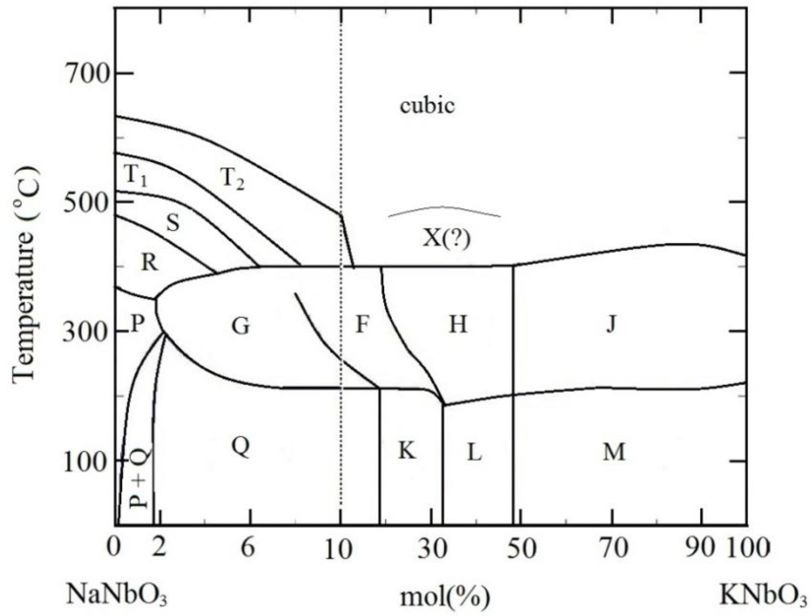
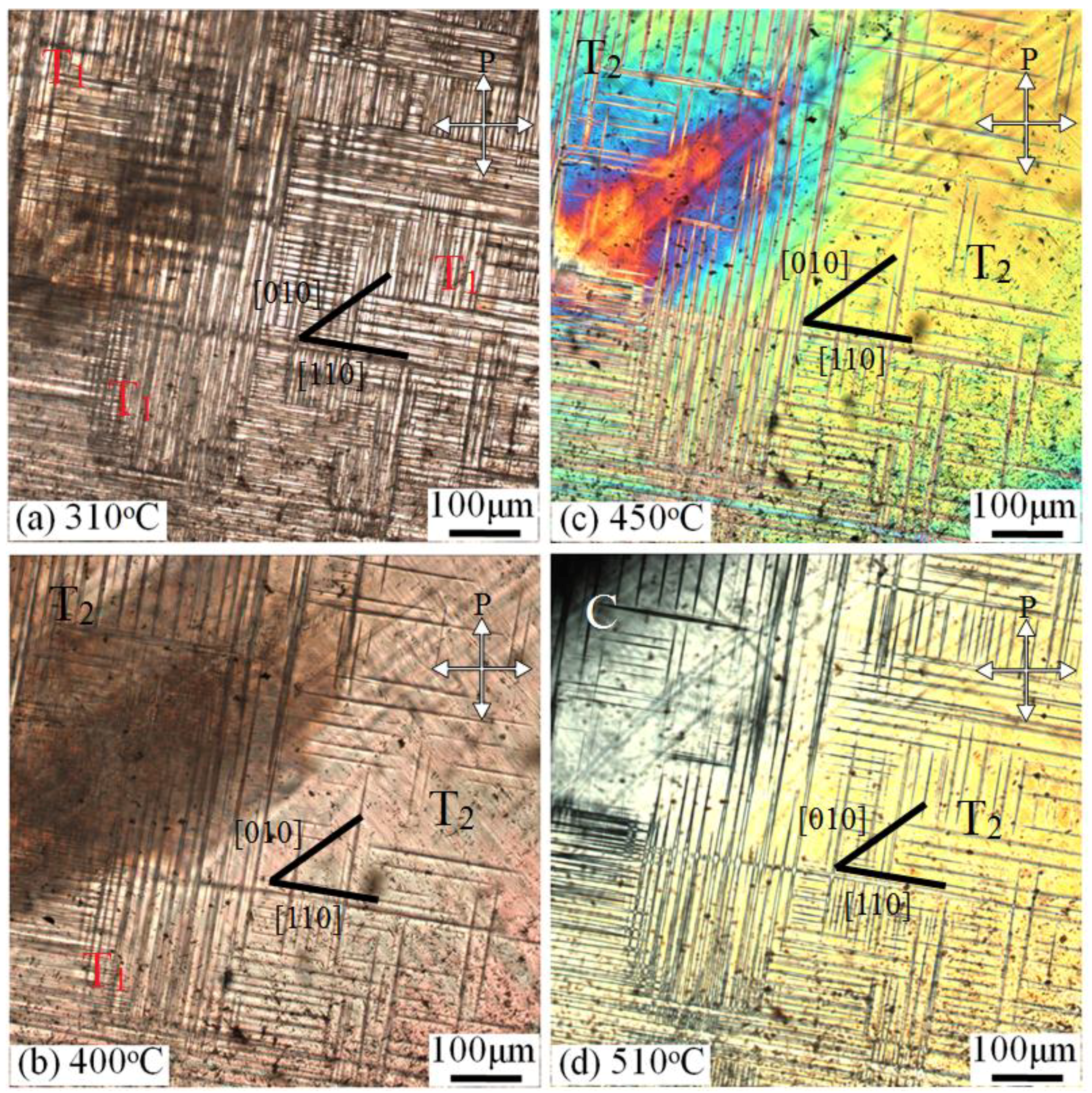
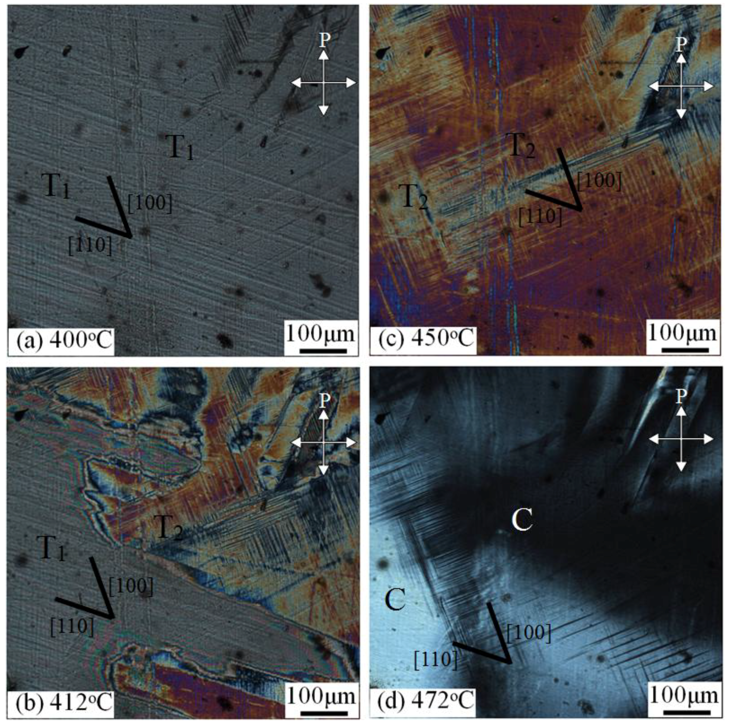
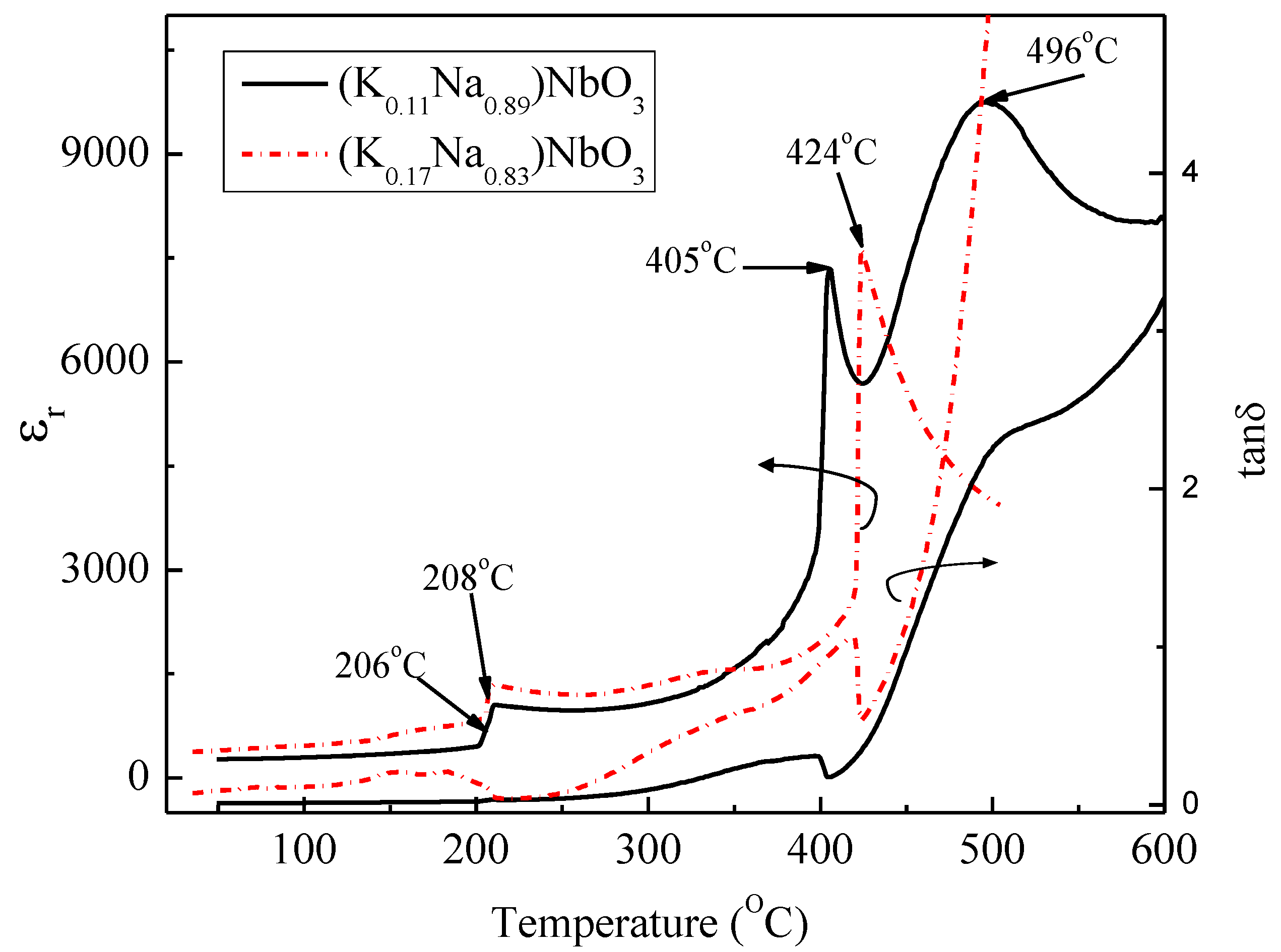
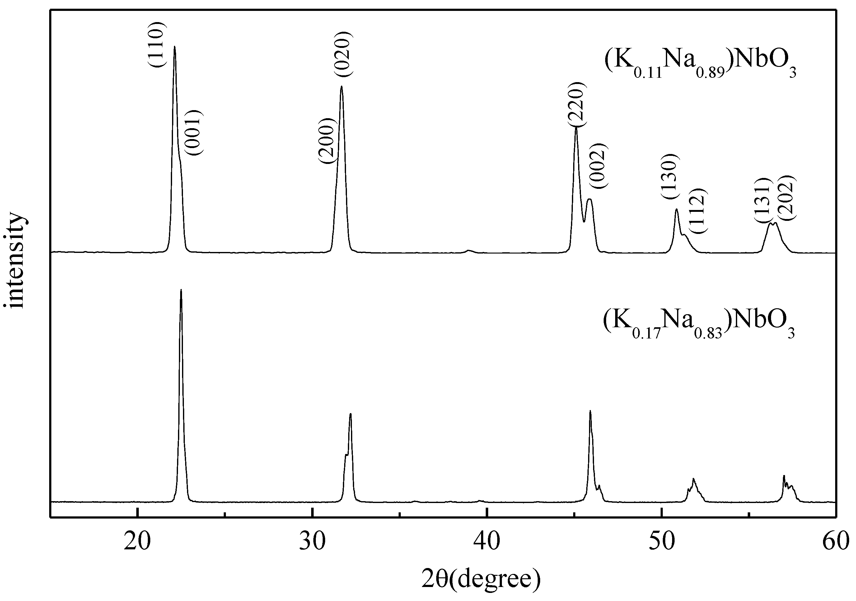
2. Results and Discussion


| Sample | Na | K | Nb | Formula |
|---|---|---|---|---|
| Raw material | 50 | 50 | 100 | (K0.5Na0.5)NbO3 |
| Sample 1 | 90.62 | 10.88 | 100 | (K0.11Na0.89)NbO3 |
| 89.65 | 11.44 | 100 | (K0.11Na0.89)NbO3 | |
| 88.76 | 12.04 | 100 | (K0.12Na0.88)NbO3 | |
| Sample 2 | 83.71 | 18.50 | 100 | (K0.18Na0.82)NbO3 |
| 83.54 | 16.76 | 100 | (K0.17Na0.83)NbO3 | |
| 82.99 | 15.77 | 100 | (K0.16Na0.84)NbO3 |


| crystals | Domain observation | Dielectric permittivity | ||
|---|---|---|---|---|
| TT1–T2 (°C) | TC (°C) | TT1–T2 (°C) | TC (°C) | |
| (K0.11Na0.89)NbO3 | 400 | 510 | 405 | 496 |
| (K0.17Na0.83)NbO3 | 412 | 472 | – | 424 |
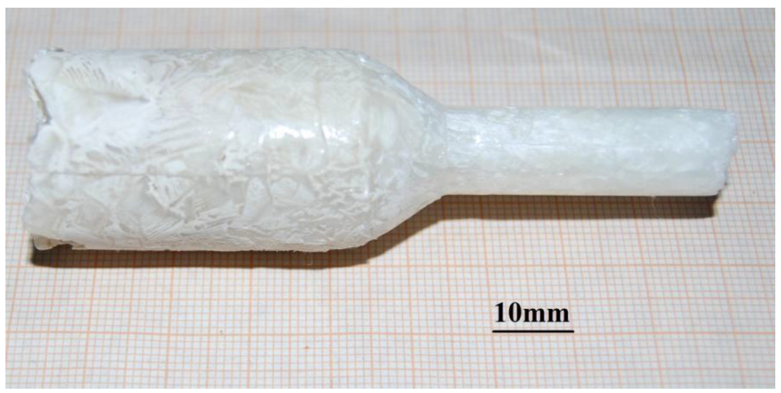
3. Experimental Section
4. Conclusions
Acknowledgments
Author Contributions
References
- Saito, Y.; Takao, H.; Tani, T.; Nonoyama, T.; Takatori, K.; Homma, T.; Nagaya, T.; Nakamura, M. Lead-free piezoceramics. Nature 2004, 432, 84–87. [Google Scholar] [CrossRef]
- Shrout, T.; Zhang, S. Lead-free piezoelectric ceramics: Alternatives for PZT? J. Electroceram. 2007, 19, 111–124. [Google Scholar]
- Du, H.; Zhou, W.; Luo, F.; Zhu, D.; Qu, S.; Pei, Z. Perovskite lithium and bismuth modified potassium-sodium niobium lead-free ceramics for high temperature applications. Appl. Phys. Lett. 2007, 91. [Google Scholar] [CrossRef]
- Wang, K.; Li, J. Domain engineering of lead-free Li-modified (K,Na)NbO33 polycrystals with highly enhanced piezoelectricity. Adv. Funct. Mater. 2010, 20, 1–6. [Google Scholar]
- Zang, G.; Wang, J.; Chen, H.; Su, W.; Wang, C.; Qi, P.; Ming, B.; Du, J.; Zheng, L.; Zhang, S.; et al. Perovskite (Na0.5K0.5)1−x(LiSb)xNb1−xO3 lead-free piezoceramics. Appl. Phys. Lett. 2006, 88. [Google Scholar] [CrossRef]
- Lin, D.; Kwok, K.; Chan, H. Microstructure, dielectric and piezoelectric properties of (K0.5Na0.5)NbO3-Ba(Ti0.95Zr0.05)O3 lead-free ceramics with CuO sintering aid. Appl. Phys. A 2007, 88, 359–363. [Google Scholar]
- Wu, J.; Xiao, D.; Wang, Y.; Zhu, J. Effects of K/Na ratio on the phase structure and electrical properties of (KxNa0.96−xLi0.04)(Nb0.91Ta0.05Sb0.04)O3 lead-free ceramics. Appl. Phys. Lett. 2007, 91. [Google Scholar] [CrossRef]
- Zhang, S.; Xia, R.; Shrout, T. Modified (K0.5Na0.5)NbO3 based lead-free piezoelectric with broad temperature usage range. Appl. Phys. Lett. 2007, 91. [Google Scholar] [CrossRef]
- Guo, Y.; Kakimoto, K.; Ohsato, H. (Na0.5K0.5)NbO3-LiTaO3 lead-free piezoelectric ceramics. Mater. Lett. 2005, 59, 241–244. [Google Scholar] [CrossRef]
- Zhang, S.; Xia, R.; Shrout, T.; Zhang, G.; Wang, J. Piezoelectric properties in perovskite 0.948(K0.5Na0.5)NbO3-0.052LiSbO3 lead-free ceramics. J. Appl. Phys. 2006, 100. [Google Scholar] [CrossRef]
- Fisher, J.; Benan, A.; Holc, J.; Kosec, M.; Vernay, S.; Rytz, D. Growth of potassium sodium niobate single crystals by solid state crystal growth. J. Cryst. Growth 2007, 303, 487–492. [Google Scholar] [CrossRef]
- Chen, K.; Xu, G.; Yang, D.; Wang, X.; Li, J. Dielectric and piezoelectric properties of lead-free 0.95(K0.5Na0.5)NbO3-0.05LiNbO3 crystals grown by the Bridgman method. J. Appl. Phys. 2007, 101. [Google Scholar] [CrossRef]
- Inagaki, Y.; Kakimoto, K. Dielectric and piezoelectric properties of Mn-doped Na0.5K0.5NbO3 single crystals grown by flux method. Appl. Phys. Expr. 2008, 1. [Google Scholar] [CrossRef]
- Lin, D.; Li, Z.; Zhang, S.; Xu, Z.; Yao, X. Influence of MnO2 doping on the dielectric and piezoelectric properties and the domain structure in (K0.5Na0.5)NbO3 single crystals. J. Am. Ceram. Soc. 2010, 93, 941–944. [Google Scholar]
- Huo, X.; Zheng, L.; Zhang, S.; Zhang, R.; Liu, G.; Wang, R.; Yang, B.; Cao, W.; Shrout, T. Growth and properties of Li, Ta modified (K,Na)NbO3 lead-free piezoelectric single crystals. Phys. Status Solidi RRL 2014, 8, 86–90. [Google Scholar] [CrossRef]
- Wada, S.; Muraoka, K.; Kakemoto, H.; Tsurumi, T.; Kumagai, H. Enhanced piezoelectric properties of potassium niobate single crystals by domain engineering. Jpn. J. Appl. Phys. 2004, 43, 6692–6700. [Google Scholar] [CrossRef]
- Wada, S.; Suzuki, S.; Noma, T.; Suzuki, T.; Osada, M.; Kakihana, M.; Park, S.; Cross, L.; Shrout, T. Enhanced piezoelectric property of barium titanate single crystals with engineered domain configurations. Jpn. J. Appl. Phys. 1999, 38, 5505–5511. [Google Scholar] [CrossRef]
- Lin, D.; Li, Z.; Zhang, S.; Xu, Z.; Yao, X. Dielectric/Piezoelectric properties and temperature dependence of domain structure evolution in lead free (K0.5Na0.5)NbO3 single crystal. Solid State Commun. 2009, 149, 1646–1649. [Google Scholar] [CrossRef]
- Lin, D.; Li, Z.; Zhang, S.; Ma, M.; Xu, Z.; Yao, X. Temperature dependence of domain structure in (K0.17Na0.83)NbO3 lead free piezoelectric single crystal grown by Bridgman method. Ferroelectrics 2010, 404, 200–206. [Google Scholar] [CrossRef]
- Shirane, G.; Newnham, R.; Pepinsky, R. Dielectric Properties and Phase Transitions of NaNbO3 and (Na,K)NbO3. Phys. Rev. 1954, 96, 581–588. [Google Scholar] [CrossRef]
- Lin, D.; Li, Z.; Xu, Z.; Yao, X. Characterization of KNN Single Crystals by Slow-Cooling Technique. Ferroelectrics 2009, 381, 1–8. [Google Scholar] [CrossRef]
- Ahtee, M.; Glazer, A. Lattice Parameters and Tilted Octahedra in Sodium-Potassium Niobate Solid Solutions. Acta Cryst. 1976, A32, 434–446. [Google Scholar] [CrossRef]
- Ivliev, M.; Raevskii, I.; Reznichenko, L.; Raevskaya, S.; Sakhnenko, V. Phase States and Dielectric Properties of Sodium-Potassium Niobate Solid Solutions. Phys. Solid State 2003, 45, 1984–1989. [Google Scholar] [CrossRef]
© 2014 by the authors; licensee MDPI, Basel, Switzerland. This article is an open access article distributed under the terms and conditions of the Creative Commons Attribution license (http://creativecommons.org/licenses/by/3.0/).
Share and Cite
Lin, D.; Li, Z.; Li, F.; Cai, C.; Liu, W.; Zhang, S. Tetragonal-to-Tetragonal Phase Transition in Lead-Free (KxNa1−x)NbO3 (x = 0.11 and 0.17) Crystals. Crystals 2014, 4, 113-122. https://doi.org/10.3390/cryst4020113
Lin D, Li Z, Li F, Cai C, Liu W, Zhang S. Tetragonal-to-Tetragonal Phase Transition in Lead-Free (KxNa1−x)NbO3 (x = 0.11 and 0.17) Crystals. Crystals. 2014; 4(2):113-122. https://doi.org/10.3390/cryst4020113
Chicago/Turabian StyleLin, Dabin, Zhenrong Li, Fei Li, Changlong Cai, Weiguo Liu, and Shujun Zhang. 2014. "Tetragonal-to-Tetragonal Phase Transition in Lead-Free (KxNa1−x)NbO3 (x = 0.11 and 0.17) Crystals" Crystals 4, no. 2: 113-122. https://doi.org/10.3390/cryst4020113
APA StyleLin, D., Li, Z., Li, F., Cai, C., Liu, W., & Zhang, S. (2014). Tetragonal-to-Tetragonal Phase Transition in Lead-Free (KxNa1−x)NbO3 (x = 0.11 and 0.17) Crystals. Crystals, 4(2), 113-122. https://doi.org/10.3390/cryst4020113