Simulation Design for Rutile-TiO2 Nanostructures with a Large Complete-Photonic Bandgap in Electrolytes

Abstract
:1. Introduction
2. Calculation
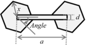
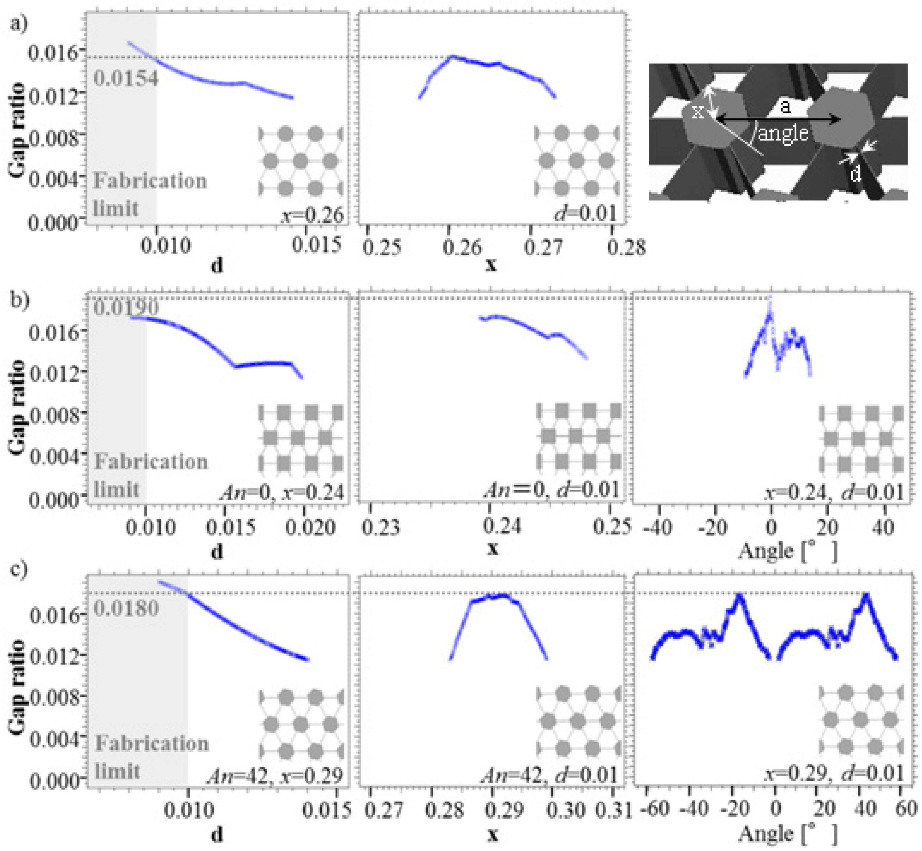
2.1. Structural Design

| Resolution | Cylindrical | Square | Hexagonal | |
|---|---|---|---|---|
| d | 1 × 10⁻⁵ | 0.00–0.50 | 0.00–0.50 | 0.00–0.50 |
| x | 1 × 10⁻⁴ | 0.01–0.50 | 0.01–0.50 | 0.01–0.50 |
| Angle [°] | 0.01 | - | (−45)–(+45) | (−60)–(+60) |
2.2. Simulation Methods
3. Results and Discussion
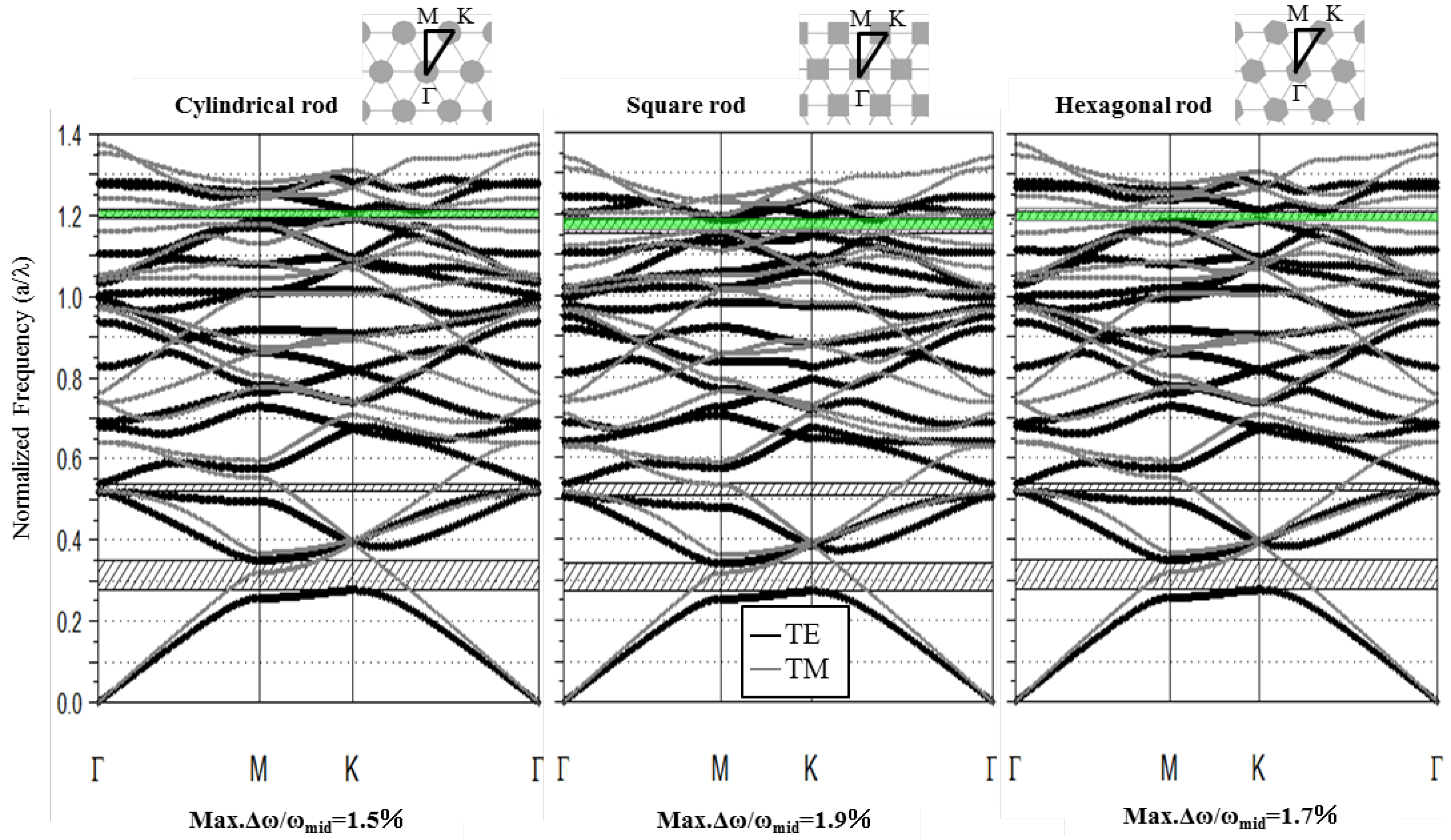
3.1. Photonic Band Diagram of Each Structure
| Shape | Cylindrical | Square | Hexagonal | |
|---|---|---|---|---|
| TE | Upper edge | K | M | K |
| Lower edge | K | M | Between M and K | |
| TM | Upper edge | K and Γ | M | Between Γ and M |
| Lower edge | K | M | K | |
3.2. Gap Ratio Change with Each Parameter

4. Conclusions
Acknowledgments
Conflict of Interest
References
- Tao, C.-A.; Zhu, W.; An, Q.; Li, G. Theoretical demonstration of efficiency enhancement of dye-sensitized solar cells with double-inverse opal as mirrors. J. Phys. Chem. C 2010, 114, 10641. [Google Scholar] [CrossRef]
- Matsushita, S.; Suavet, O.; Hashiba, H. Full-photonic-bandgap structures for prospective dye-sensitized solar cells. Electrochim. Acta 2010, 55, 2398–2403. [Google Scholar] [CrossRef]
- Guldin, S.; Hüttner, S.; Kolle, M.; Welland, M.E.; Müller-Buschbaum, P.; Friend, R.H.; Steiner, U.; Tétreault, N. Dye-sensitized solar cell based on a three-dimensional photonic crystal. Nano Lett. 2010, 10, 2303–2309. [Google Scholar] [CrossRef]
- Kwak, E.S.; Lee, W.; Park, N.-G.; Kim, J.; Lee, H. Compact inverse-opal electrode using non-aggregated TiO2 nanoparticles for dye-sensitized solar cells. Adv. Funct. Mater. 2009, 19, 1093–1099. [Google Scholar] [CrossRef]
- Colodrero, S.; Mihi, A.N.; Häggman, L.; Ocaña, M.; Boschloo, G.; Hagfeldt, A.; Míguez, H.N. Porous one-dimensional photonic crystals improved the power-conversion efficiency of dye-sensitized solar cells. Adv. Mat. 2009, 21, 764–770. [Google Scholar] [CrossRef]
- Mihi, A.; Calvo, M.E.; Anta, J.A.; Miguez, H. Spectral response of opal- based dye-sensitized solar cells. J. Phys.Chem. C 2008, 112, 13–17. [Google Scholar]
- Lee, S.-H.A.; Abrams, N.M.; Hoertz, P.G.; Barber, G.D.; Halaoui, L.I.; Mallouk, T.E. Coupling of titania inverse opals to nanocrystalline titania layers in dye-sensitized solar cells. J. Phys. Chem. B 2008, 112, 14415–14421. [Google Scholar] [CrossRef]
- Matsushita, S.I.; Fukuda, N.; Shimomura, M. Photochemically functional photonic crystals prepared by using a two-dimensional particle-array template. Colloid. Surf. A 2005, 257-258, 15–17. [Google Scholar] [CrossRef]
- Matsushita, S.; Fujiwara, R.; Shimomura, M. Calculation of photonic energy bands of self-assembled-type TiO2 photonic crystals as dye-sensitized solar battery. Colloid. Surf. A 2008, 313-314, 617–620. [Google Scholar] [CrossRef]
- Mihi, A.; Calvo, M.E.; Anta, J.A.; Miguez, H. Spectral response of opal-based dye-sensitized solar cells. J. Phys.Chem.C 2008, 112, 13–17. [Google Scholar] [CrossRef]
- Yablonovitch, E. Inhibited spontaneous emission in solid-state physics and electronics. Phys. Rev. Lett. 1987, 58, 2059–2062. [Google Scholar] [CrossRef]
- John, S. Strong localization of photons in certain disordered dielectric superlattices. Phys. Rev. Lett. 1987, 58, 2486–2489. [Google Scholar] [CrossRef]
- Usami, A. Theoretical study of application of multiple scattering of light to a dye-sensitized nanocrystalline photoelectrichemical cell. Chem. Phys. Lett. 1997, 277, 105. [Google Scholar] [CrossRef]
- Nishimura, S.; Abrams, N.; Lewis, B.A.; Halaoui, L.I.; Mallouk, T.E.; Benkstein, K.D.; Lagemaat, J.V.D.; Frank, A.J. Standing wave enhancement of red absorbance and photocurrent in dye-sensitized titanium dioxide photoelectrodes coupled to photonic crystals. J. Am. Chem. Soc. 2003, 125, 6306–6310. [Google Scholar]
- Rehm, J.M.; McLendon, G.L.; Nagasawa, Y.; Yoshihara, K.; Moser, J.; Gratzel, M. Femtosecond electron-transfer dynamics at a sensitizing dye-semiconductor (TiO2) interface. J. Phys. Chem. 1996, 100, 9577–9578. [Google Scholar]
- Shimomura, M.; Matsushita, S.; Fukuda, N. Photon-to-electron conversion devices and the aplication to the solar cells. Japanese Unexamined Patent Application Publication 2005-72524, 2005. [Google Scholar]
- Ritari, T.; Tuominen, J.; Ludvigsen, H.; Petersen, J.C.; Sørensen, T.; Hansen, T.P.; Simonsen, H.R. Gas sensing using air-guiding photonic bandgap fibers. Opt. Express 2004, 12, 4080–4087. [Google Scholar] [CrossRef]
- Chen, J.S.Y.; Euser, T.G.; Farrer, N.J.; Sadler, P.J.; Scharrer, M.; Russell, P.S.J. Photochemistry in photonic crystal fiber nanoreactors. Chem. Eur. J. 2010, 16, 5067–5612. [Google Scholar]
- Oh, S.H.; Kim, J.G.; Kim, C.S.; Chang, S.; Lee, S.; Jeong, M.Y. The fabrication of three-dimensional nano-structures by defocused electron beam energy. Microelectron. Eng. 2011, 88, 914–922. [Google Scholar] [CrossRef]
- Chern, R.-L.; Chang, C.-C.; Chang, C.C.; Hwang, R.R. Two classes of photonic crystals with simultaneous band gaps. Jpn. J. Appl. Phys. 2004, 43, 3484–3490. [Google Scholar] [CrossRef]
- Joannopoulos, J.D.; Johnson, S.G.; Winn, J.N.; Meade, R.D. Photonic Crystals: Molding the Flow of Light; Princeton University Press: New Jersey, NJ, USA, 2008. [Google Scholar]
- Marsal, L.F.; Trifonov, T.; Rodriguez, A.; Pallares, J.; Alcubilla, R. Larger absolute photonic band gap in two-dimensional air-silicon structures. Physica E 2003, 16, 580–585. [Google Scholar] [CrossRef]
- Wang, X.H.; Gu, B.Y.; Li, Z.Y.; Yang, G.Z. Large absolute photonic band gaps created by rotating noncircular rods in two-dimensional lattices. Phys. Rev. B 1999, 60, 11417. [Google Scholar]
- Chern, R.L.; Chang, C.C.; Chang, C.; Hwang, R.R. Large full band gaps for photonic crystals in two dimensions computed by an inverse method with multigrid acceleration. Phys. Rev. E 2003, 68, 026704. [Google Scholar] [CrossRef]
- Liu, W.-L.; Yang, T.-J. Engineering the bandgap of a two-dimensional photonic crystal with slender dielectric veins. Phys. Lett. A 2007, 369, 518–523. [Google Scholar] [CrossRef]
- Qiu, M.; He, S. Optimal design of a two-dimensional photonic crystal of square lattice with a large complete two-dimensional bandgap. J. Opt. Soc. Am. B 2000, 17, 1027–1030. [Google Scholar] [CrossRef]
© 2012 by the authors; licensee MDPI, Basel, Switzerland. This article is an open-access article distributed under the terms and conditions of the Creative Commons Attribution license (http://creativecommons.org/licenses/by/3.0/).
Share and Cite
Matsushita, S.; Hayashi, M.; Isobe, T.; Nakajima, A. Simulation Design for Rutile-TiO2 Nanostructures with a Large Complete-Photonic Bandgap in Electrolytes. Crystals 2012, 2, 1483-1491. https://doi.org/10.3390/cryst2041483
Matsushita S, Hayashi M, Isobe T, Nakajima A. Simulation Design for Rutile-TiO2 Nanostructures with a Large Complete-Photonic Bandgap in Electrolytes. Crystals. 2012; 2(4):1483-1491. https://doi.org/10.3390/cryst2041483
Chicago/Turabian StyleMatsushita, Sachiko, Mikiro Hayashi, Toshihiro Isobe, and Akira Nakajima. 2012. "Simulation Design for Rutile-TiO2 Nanostructures with a Large Complete-Photonic Bandgap in Electrolytes" Crystals 2, no. 4: 1483-1491. https://doi.org/10.3390/cryst2041483
APA StyleMatsushita, S., Hayashi, M., Isobe, T., & Nakajima, A. (2012). Simulation Design for Rutile-TiO2 Nanostructures with a Large Complete-Photonic Bandgap in Electrolytes. Crystals, 2(4), 1483-1491. https://doi.org/10.3390/cryst2041483