Abstract
Developing detectors to enhance the timing resolution of positron emission tomography scanners can help reduce radioactive doses absorbed by patients and improve spatial resolution in medical imaging. Time resolution may be enhanced in heterostructures comprising a heavy scintillator for attenuation of 511 keV γ-quanta, as well as a fast scintillator converting recoiled electrons from the heavy scintillator to prompt light photons. In this study, ZnO films as fast scintillators with different thicknesses were obtained on substrates of a heavy bismuth germanate (Bi4Ge3O12, BGO) scintillator using several film preparation techniques, such as spray-coating, drop-casting, and spin-coating. The design of heterostructures combined the key advantage of a low-cost film preparation technique with environmentally friendly and available precursors. This work proposes synthesis methods of highly nanocrystalline ZnO films on BGO, where a film thickness ranges from 6 to 18 μm. All ZnO studied films exhibit exciton luminescence peaked in UV (353 nm) and defect luminescence in the green (657 nm) range under 325 nm excitation. The best coincidence time resolution of 158 ± 8 ps was obtained with BGO@ZnO heterostructures fabricated by the spray-coating. The proposed approach allowed obtaining BGO@ZnO heterostructures for potential use as ultrafast scintillation detectors.
1. Introduction
Positron emission tomography (PET) is the most efficient tool to identify tumors in the human body. The principle of Time-of-Flight PET (TOF-PET) is based on the detection of γ-quanta generated by electron-positron annihilation in a certain area belonging to a tumor; herein, two detectors register γ-quanta born in the same annihilation event and emitted in the opposite directions. Meanwhile, spatial resolution of images is limited by both the delayed response of scintillation detectors to generated γ-quanta, and the metabolism of the tracer molecule in the patient’s body. Scintillation detectors with improved timing performance should enhance TOF-PET sensitivity and reduce radioactive doses injected into patients [1]. Researchers face a similar problem in particle physics experiments. Recently, the experiments at the Large Hadron Collider (LHC) in CERN contributed to the experimental confirmation of the existence of the Higgs boson [2]. A significant increase in the accelerator luminosity and the frequency of particle collisions is underway at the upgraded LHC, requiring high-speed detection systems [3]. Ultrafast scintillation detectors are necessary to avoid pile-up and incorrect association of particle tracks with vertices in particle physics experiments.
The coincidence time resolution (CTR) of a detector quantifies the precision of timing information in TOF-PET. Following the analytical relationship for CTR and scintillation parameters of a material [4], the scintillation rise (τrise) and decay (τdecay) times should be as short as possible. In contrast, light output (LO) in this time interval should be as high as possible (Equation (1)). According to the estimations [5], a CTR of 10 ps may be achieved in a scintillation material with a light yield of at least several thousand photons/MeV and rise and decay times in the subnanosecond domain. There are no existing monolithic scintillators meeting these requirements.
In conventional PET scanners, the CTR is approximately 500 ps, corresponding to an imprecision of ~7.5 mm in the event localization at the origin of the emission of the two γ-rays along the response line [1]. In the conditions of a low timing resolution, uncorrelated particles are collected within each interval, creating false readings. With the existing state-of-the-art homogeneous scintillators and photodetectors, CTR is limited by ~100 ps due to low light yield and/or slow luminescence rise/decay times [1]. According to the estimations [5], a time resolution of ~10 ps is necessary for a spatial resolution of 1–2 mm. High CTR is, therefore, vitally important for medical imaging. Heterostructure with fast rise and decay times should result in a more stable working trigger point, lower channel deskew, and hence better CTR.
The problem of improving the timing resolution of detectors involves several aspects, namely the radiation detection material itself, the geometry of the detector to collect as much light as possible, and the dedicated electronics operating near the limit of counting statistics. None of the existing scintillators is capable of providing the mentioned performance. While heavy and bright scintillators with activator luminescence, such as Lu1−xYxSiO5:Ce (LYSO:Ce), Gd3Al5−xGaxO12:Ce, YAlO3:Ce, and SrI2:Eu cannot provide luminescence decay times below 20–40 ns, while the light output of fast scintillators based on other mechanisms, such as Cherenkov radiation, quantum confinement, or intraband luminescence, etc., usually does not exceed a few hundred photons per MeV [6].
Meanwhile, recent studies [7,8,9] demonstrated a chance to overcome such limitations with heterostructures combining a heavy scintillator that absorbs high-energy particles and a light and fast light scintillator converting secondary carriers generated in a heavy scintillator into prompt photons. According to the timeline of a scintillation process upon the incidence of the ionizing particle [10], it involves the cascade of inelastic electron scattering (10−16–10−14 s) followed by the thermalization of hot carriers (10−14–10−12 s), the capture of electrons and holes by carrier traps (10−12–10−10 s), and the transport of excitations and emission of photons (10−10–10−7 s). Hence, the idea of a heterostructure scintillator is to attenuate incident particles by inelastic scattering in a heavy scintillator, while the generated recoil electrons are absorbed by a fast scintillator where all the subsequent stages of the scintillation process will take as little as a few ns.
Many scientific reports are devoted to efficient heavy scintillators based on oxide compounds. However, the research mainly focused on oxyorthosilicate Lu1−xYxSiO5:Ce (LYSO:Ce) and bismuth germanate Bi4Ge3O12 (BGO) single crystals currently used in conventional TOF-PET [1]. Several types of fast scintillators capable of providing the mentioned speed of scintillation response have been studied recently, such as plastics [7,9] and CdS/CdSe [8]. A CTR of 95 ps for one-third of the events at 511 keV excitation was achieved in the BGO + BC-422 heterostructure pixel. The other two-thirds of the 511 keV events performed similarly to standard BGO crystals, with a time resolution of around 117 ps (equivalent to a CTR of 165 ps). The CTR of 55 ps was achieved with shared events in the case of LYSO + BC-422 pixel [7]. CTRs of 239 ± 12 ps and 197 ± 10 ps were obtained, respectively, with the 15 mm long heterostructures where 100 mm- and 200 mm-thick plates of EJ232 plastic scintillator alternate with 100 mm thick BGO plates. For comparison, the CTR values of 271 ± 14 ps and 303 ± 15 ps were obtained for bulk and layered BGO, respectively [9]. Heterostructure LYSO:Ce + CdSe nanoplatelets provided a CTR of 80 ps [8]. Meanwhile, the two-dimensional (2D) perovskite crystals, CsPbX3 (X = Br, Cl, I), are considered promising for such applications due to a relatively high density, short luminescence lifetimes of 0.6–17.0 ns, and a good tunability of the luminescence band, as well as scintillation parameters depending on the anionic composition [11,12]. These values make this type of compound among the fastest scintillators, while the light yield in some reaches 40,000 photons/MeV.
The main disadvantages of the given fast scintillators are their low density and stopping power (plastics), causing a low registration efficiency, and/or poor chemical stability and radiation hardness (perovskites). Meanwhile, scintillators based on semiconductors like ZnO and ZnO:Ga, with a high density of 5.61 g/cm3, may be the alternative fast scintillators. ZnO, with remarkable electrical and optical properties, is a transparent conductive material. Furthermore, ZnO is chemically stable and unhygroscopic, with an energy gap of 3.37 eV at room temperature and an exciton binding energy of 60 meV. These characteristics enable good luminescence band tunability [13]. ZnO exhibits high radiation hardness, see, for example, refs. [14,15] due to a large threshold displacement energy for damage because of the small unit-cell volume and large bandgap energy. Long-term stability of such films should be addressed in more detail, but we expect a significantly longer lifetime compared to plastics and perovskites. ZnO properties can be easily tuned by doping with n-type and p-type impurities; in particular, Ga3+ ions enhance scintillation efficiency: ZnO:Ga, along with BaF2, exhibits the ultrafast luminescence rise/decay times of 0.2 ns/0.5 ns [15,16] that may improve the registration efficiency of heterostructures. Hence, BGO@ZnO heterostructures, with BGO as a heavy scintillator with a 7.13 g/cm3 density and Zeff = 74 [17], are potentially superior to the abovementioned heterostructures.
Different geometries of heterostructure detectors are considered to provide higher attenuation of particles while keeping the volume fraction of a fast scintillator as high as possible to increase the number of events shared between these two materials and to provide a fast scintillation process. They include alternating layers of heavy and light scintillators [7,8,9], heavy scintillators with holes filled with light scintillators [18,19], and 3D printing of complex geometries [20]. According to modeling predictions, the optimal registration efficiency is expected when the thickness of alternating layers is within tens to hundreds of μm [21,22].
Physical and chemical methods are used to obtain ZnO films: pulsed-laser deposition (PLD) [23,24], magnetron sputtering [25], spray pyrolysis [26], drop casting, and different chemical methods, mainly based on the sol–gel process [27]. These methods allow obtaining high-quality films with controlled thicknesses. The microstructure, transparency, and morphology of ZnO films are caused by growth methods and post-heat treatment parameters. Meanwhile, among chemical methods, the sol–gel process of film preparation by the spin- or deep-coating is a facile, reproducible, and preferable approach to obtaining high-quality material with appropriate characteristics, which allows controlling film parameters at each stage of film preparation as compared to expensive and often time-consuming physical methods.
This work explores the potential of BGO@ZnO heterostructures, with BGO and ZnO as heavy and fast scintillators, respectively, for potential use as ultrafast γ-ray detection. ZnO films of different thicknesses were successfully obtained using spin-coating, drop-casting, and spraying techniques on BGO substrates. The morphology, structure, and CTR of BGO@ZnO were explored.
2. Materials and Methods
Raw Materials: Bi2O3 and GeO2 powders (99.999%, Wuhan Xinrong New Materials Co., Ltd., Wuhan, China) were used as starting materials for BGO crystal growth. Zinc acetate dihydrate (Zn(CH3COO)2.2H2O, Sigma Aldrich, St. Louis, MO, USA), sodium hydroxide (NaOH, Stanlab), mono-ethanolamine (MEA, C2H7NO, 99%, Sigma Aldrich), 2-methoxyethanol (C3H8O2, 99.5%, Sigma Aldrich), methanol, and ethanol were used as starting materials for the preparation of ZnO precursor solutions. Materials were used as obtained without further purification.
Fabrication of heavy scintillator (BGO) wafers: The synthesis of Bi4Ge3O12 crystals began with the ball-milling of stoichiometric amounts of 5N pure Bi2O3 and GeO2 in a molar ratio corresponding to Bi4Ge3O12. This mixture was then loaded into a platinum crucible and subjected to a controlled heating process, reaching 800 °C over 4 h, followed by a 10 h dwell time. This thermal treatment ensured the complete reaction of starting materials and the formation of the desired compound. The resulting charge was crushed, remixed, and transferred to a separate platinum crucible (45 mm height, 50 mm outer diameter, and 2 mm thickness). Crystals were grown on a <1 0 0> crystallographic-oriented Bi4Ge3O12 seed using a Cyberstar Czochralski growth apparatus equipped with a resistive heating furnace and computerized heating control. Following complete melting of the charge, a 2 h homogenization period ensured uniformity of the melt. Through multiple growth experiments, an optimal pulling rate of 1.5 mm/h and a rotation rate of 15–20 rpm were determined. High-quality Bi4Ge3O12 crystals of 25 mm diameter and 60 mm length were successfully grown in an air atmosphere. Finally, the crystals were sawn into 10 × 5 mm2 wafers with thicknesses of several hundred μm. The wafer surfaces were left unpolished to provide better adhesion of ZnO films.
2.1. Preparation of ZnO Sol–Gel Films on BGO Substrates
Sol–gel preparation of ZnO precursors: Sol–gel technology has been successfully applied to obtaining ZnO films. The ZnO films were obtained in several ways. The solutions for ZnO film spin-coating preparation were obtained in two ways. In the first case (Precursor 1), zinc acetate dehydrate was dissolved in 2-methoxyethanol at room temperature with the 0.75 M concentration of zinc acetate to prepare a sol–gel precursor stabilized by MEA [28]. The MEA to Zn molar ratio was 1.0. The resultant solution was stirred at 80 °C for 200 min to yield a clear, transparent, and homogeneous solution maintained for 30 h.
Sol–gel preparation of ZnO nanoparticles: In the second case (Precursor 2), we used a solution of crystalline ZnO nanoparticles (NPs) prepared by the low-temperature sol–gel route [29]. ZnO NPs were synthesized by dissolving 13.4 mmol of Zn((CH3COO)2.2H2O) in 125 mL of methanol at 60 °C. Then, 23 mmol of NaOH dissolved in 65 mL of methanol was added to zinc acetate dihydrate. White ZnO nanoparticles were separated from the mother liquor after 3 h, washed twice with methanol, and dried to the condition of a white powder.
ZnO film preparation: In our research, ZnO films on BGO substrates were obtained from these two types of precursors using different deposition techniques: spin-coating, drop-casting, and spraying. For the spin-coating approach, a POLOS and SPS (SPS Polos, Munich, Germany) spin coater was used. Before ZnO film coating, BGO substrates were cleaned in acetone and ethanol. Precursor 1 was used for ZnO film preparation using spin-coating and drop-casting approaches. Precursor 1 was spin-coated on a rotated BGO substrate at 2000 rpm for 20 s. The coating and baking procedure was repeated 10 times. After each layer deposition, the substrate was put on a hotplate heated to 250 °C for 15 min to remove organic residuals. Finally, the obtained film was annealed at 500 °C for 100 min in a flowing nitrogen atmosphere (Sample 1).
In the drop-casting approach, ZnO film was obtained using Precursor 1 by dropping ZnO-based solution on BGO substrate (3 cycles (1 cycle—20 µL)). The ZnO layer was dried at 60 °C for 30 min after each cycle. The ZnO crystal phase in the film was obtained by annealing at 500 °C for 100 min in a flowing nitrogen atmosphere (Sample 2).
Precursor 2 (crystalline ZnO NPs) was used for ZnO film preparation using spin-coating, drop-casting, and spraying approaches. ZnO nanoparticles were dissolved in solution (ethanol:H2O, 3:1) under ultrasonication. For spin-coated film preparation, the solution with 1 mg/mL concentration was put during 20 s on the BGO substrate rotating at 2000 rpm (Sample 3). For the drop-casting ZnO film preparation, the solution of Precursor 2 was dropped on the BGO substrate in three cycles (1 cycle—20 µL), and the ZnO layer was dried at 60 °C for 30 min after each cycle (Sample 4). For the spraying approach, a ZnO-based solution was sprayed on a BGO substrate in three cycles; the ZnO layer was dried at 60 °C for 30 min after each cycle (Sample 5). The final BGO@ZnO heterostructures were dried at 60 °C for 1 h and then annealed at 200 °C for 2 h to achieve better adhesion of ZnO layers on BGO substrates. The schematic illustration of the film preparation processes is presented in Figure 1.
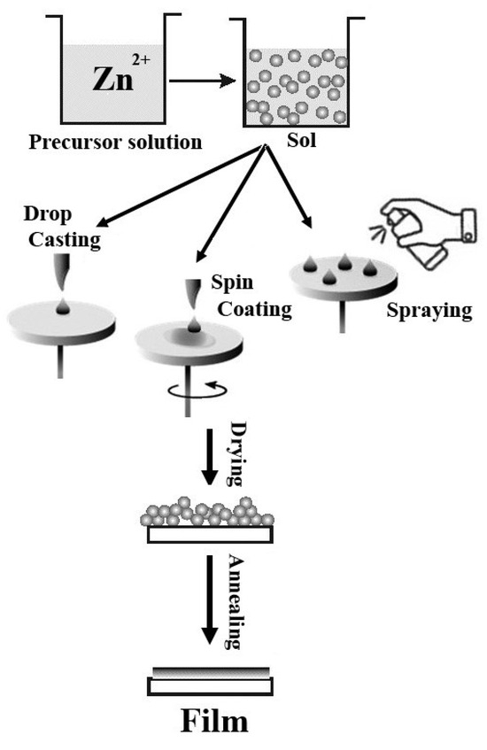
Figure 1.
Scheme of ZnO film preparation methods on a BGO substrate.
The conditions for sample preparation are summarized in Table 1.

Table 1.
Summarized experimental conditions for sample preparation.
2.2. Characterization
Morphology and structure of BGO@ZnO heterostructures: The morphology of the obtained ZnO nanoparticles and BGO@ZnO heterostructures was studied by a high-resolution transmission electron microscope ARM 200F and a JSM-7001F scanning electron microscope, both produced by JEOL (Tokyo, Japan. Results on powder X-ray diffraction (XRD) of BGO@ZnO heterostructures obtained by different methods were carried out on an Empyrean (PANalytical, Malvern, WR14 1XZ, UK) diffractometer using Cu Ka radiation (λ = 1.54 Å). Scans were recorded at room temperature (300 K) in angles ranging from 20 to 80 (°2Theta) with a step size of 0.006 and continuous scan mode. The crystallite size was calculated using the Scherrer equation. The calculation was performed over three planes from the zinc oxide X-ray diffraction pattern ((100), (002), and (101)), and the average value in angstroms was taken.
Determination of optical properties and coincidence time resolution: The absorption spectra of the samples were measured using a PerkinElmer LAMBDA 650 UV/VIS spectrophotometer equipped with a deuterium and halogen lamps covering the wavelength range from 190 nm to 900 nm. The photoluminescence (PL) data were recorded using a He-Cd laser (325 nm) with a QE65 Ocean Optics USB spectrometer operating in the 200–1100 nm spectral range.
The CTR was measured at CERN with a dedicated setup exploiting high-frequency electronics. The prepared samples were mounted horizontally and attached to MPPCs as shown in Figure 2. The scintillator was mounted horizontally on the MPPC (NUV MT 4 × 4 SiPM) without and with optical contact using the optical grease (“Pate 7”, Rhodorsil silicon compound with n = 1.41). The detector stack consists of an AFBR-S4N44P164M 4 × 4 NUV-MT MPPC of 4 × 4 mm size produced by Broadcom attached to PCB with optical silicon grease RHODORSIL® PASTE 7 (n = 1.41), additionally wrapped with PTFE tape to achieve a better light collection. A Na-22 source (1.4 MBq) was attached between the sample and a reference detector LSO:Ce:Ca 3 × 2 × 2 mm3.

Figure 2.
Detector stack.
The experimental setup (Figure 3) involves two detectors (for the studied and reference crystals), each with a two-channel readout: energy and timing. Signals from the channels were accumulated by a LeCroy DDA 735Zi fast oscilloscope (Chestnut Ridge, NY, USA) for further analysis. The setup was installed inside the black box with a constant temperature of about 18 °C. An LSO:Ce:Ca crystal with the 3 × 2 × 2 mm3 dimensions, all sides polished, produced by Siemens, was taken as reference.

Figure 3.
Experimental test bench.
The experimental exposition for each prepared sample was 24 h. Further data analysis was performed with custom scripts based on Python 3.13 release.
3. Results and Discussion
3.1. Characterization of ZnO Nanoparticles
The shape, size, and crystal structure of the crystalline ZnO NPs obtained using Precursor 2 were characterized by SEM and XRD. HRTEM images (Figure 4a) indicate that the obtained individual ZnO nanoparticles in solution for film preparation have a perfect spherical shape and uniform size distribution, with the mean nanoparticle size of about 7 nm (Figure 4a, inset). In general, the ZnO synthesis is based on the hydrolysis of zinc salts (mainly zinc acetate) in the basic solution [29]. In our research, ZnO NPs were obtained by the sol–gel technique, which is simple, performed at low temperatures, does not use sophisticated equipment, and, importantly, provides us with high-quality materials with controlled parameters. As-obtained ZnO NPs were polycrystalline. All the diffraction peaks (Figure 4b) correspond to the main (100), (002), (101), (102), (110), (103), (112), and weak (202) crystal planes corresponding to the hexagonal wurtzite ZnO structure with P63mc space group (corresponding to the standard crystallographic data in the ICDD PDF-5+ (2024), reference code: 04-013-7122).
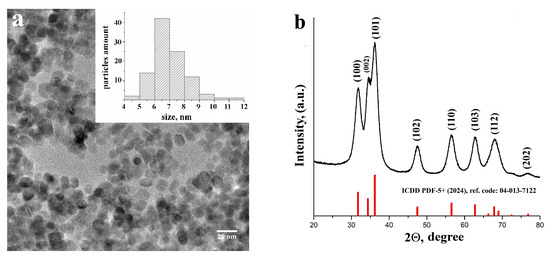
Figure 4.
HRTEM images of the ZnO NPs (a), inset—size distribution; XRD data of as-obtained ZnO NPs (b).
3.2. Morphology of BGO@ZnO Heterostructures
The chemical techniques are cheapest and safest methods of film preparation by deposition, which can be implemented easily in a standard laboratory. Sol–gel technology mainly offers the possibility of producing high-quality homogeneous thin films with controlled chemical composition in a friendly environment [29,30].
Figure 5 illustrates the morphology of ZnO film on BGO substrate obtained by spin-coating using Precursor 1 (Sample 1). The ZnO surface is relatively smooth and consists of grains with a size of approximately 100 nm (Figure 5a). The thickness of the obtained ZnO film was about 6.0 µm (Figure 5b).
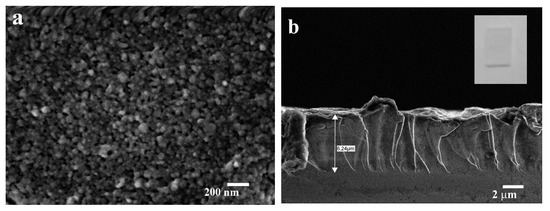
Figure 5.
SEM images of BGO@ZnO heterostructures obtained by sol–gel spin-coating approach (Sample 1): ZnO surface (a), the cross-section of ZnO film (b). Inset in (b) presents common view of the heterostructure.
The sol–gel spin coating approach generally allows for the obtaining of high-quality thin films. As mentioned in the Introduction, modeling predicted optimal scintillation efficiency when heavy/light scintillator layers comprise tens of μm [21,22]. To obtain thicker films, we used a simple approach like drop-casting (Sample 2). However, obtaining a uniform layer and controlling its thickness using drop-casting is complicated compared to the spin-coating technique.
The ZnO surface in Sample 2 is less homogeneous than that in Sample 1, consisting of spherical globules with a size of approximately 100 nm (Figure 6a). The film’s mean thickness slightly exceeded 8.0 µm (Figure 6b).
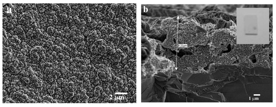
Figure 6.
SEM images of the BGO@ZnO heterostructures obtained by a sol–gel drop-casting approach using Precursor 1 (Sample 2): ZnO surface (a), a cross-section of ZnO film (b). Inset in (b) presents common view of the heterostructure.
For the preparation of ZnO film on BGO substrates using ZnO NPs (Precursor 2) and spin-coater, the obtained solution was deposited on a rotating BGO substrate (Sample 3). The ZnO surface consists of polydisperse spherical particles with a size of approximately 900 nm (Figure 7a). The film surface was not homogeneous with a mean thickness of about 12 µm (Figure 7b).

Figure 7.
SEM images of the BGO@ZnO heterostructures obtained by a sol–gel spin-coating approach using precursor ZnO NPs (Sample 3): ZnO surface (a), a cross-section of ZnO film (b). Inset in (b) presents a common view of the heterostructure.
Cracks in ZnO films deposited on BGO substrates using a drop-casting approach appeared after annealing (Sample 4) (Figure 8a,b). The thickness of the obtained ZnO film was about 18 µm (Figure 8c).

Figure 8.
SEM images of the BGO@ZnO heterostructures obtained by the sol–gel drop-casting approach (Sample 4): ZnO surface (a,b), cross-section of the ZnO film (c). Inset in (c) presents a common view of the heterostructure.
ZnO films obtained on BGO substrates using a spraying approach (Sample 5) had a unique porous structure after annealing (Figure 8). The thickness of the obtained ZnO film was about 10 µm (Figure 9).
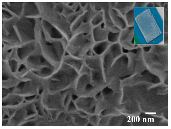
Figure 9.
SEM images of the ZnO surface in the BGO@ZnO heterostructure obtained by sol–gel spraying approach (Sample 5). Inset presents a common view of the heterostructure.
3.3. Crystalline Structure of Obtained Heterostructures
The XRD results in Figure 10 confirmed the crystalline nature of all components within the obtained heterostructures. The diffractograms exhibit characteristic reflections from the BGO substrate, specifically at 26.7°, 38.5°, and 50.5°, corresponding to the (001), (002), and (003) planes, respectively. Additionally, the diffractograms reveal prominent diffraction peaks associated with the hexagonal wurtzite ZnO structure (P63mc space group), including the (100), (002), (101), (102), (110), (103), and (112) planes, as well as weaker peaks corresponding to the (201), (200), (004), and (202) planes. These findings are consistent with standard crystallographic data (ICDD PDF-5+, 2024, reference code: 04-002-0311). Notably, no diffraction peaks from additional phases were detected, indicating the pure single phase of the synthesized materials and validating the proposed synthesis approach.

Figure 10.
XRD data of ZnO films obtained on BGO substrate by different methods.
All diffraction peaks are narrow except those for Sample 5. The broad peaks for Sample 5 may be related to the small crystallite size, while large crystallite sizes in Samples 2–4 confirm their better crystallinity. In addition, the broadening of the peaks in Sample 5 can also be attributed to an increase in defects caused by dislocations or vacancies (see Section 3.4, Optical and Luminescent Properties). The appearance of dislocations and the concentration of defects of various types may be associated with the technology of film production, including parameters such as synthesis temperatures and post-treatment, pressure, particle falling energy, etc. The intensive peaks corresponding to BGO in Samples 1, 2, and 5 were observed as well owing to the small thickness of the ZnO layers.
Indeed, temperature is one of the fundamental parameters controlling the mechanisms of formation, growth, and crystalline stability in materials. Even so, the highest temperature is not always the key to the best crystallinity. R. Ananthakrishnan and K. Goswami [31], for example, studied the impact of calcination temperature on the structure and photocatalytic activity of a bi-phase ZnO/ZnCo2O4 material. As they demonstrated, the temperature around 500 °C enables the formation of a material with the best crystallinity, structural stability, and highest photocatalytic activity. To put it briefly, optimal temperature selection allows precise tuning of material properties, even at the expense of crystallinity.
The ZnO crystal structure was verified by the Rietveld technique using FullProf software (Program FullProf.2k (Version 7.95-Jan2023-ILL JRC)), employing XRD data obtained from the heterostructures obtained by the various methods of synthesis. The refinements were based on the hexagonal unit cell with space group P63mc, where “Zn” occupies the 2b site at 1/3, 2/3, 0, and “O” occupies the 2b site at 1/3, 2/3, z. To enhance the refinement, reflections from the BGO substrate were excluded. The observed and calculated profiles showed an excellent fit, resulting in nearly flat difference profiles, which explain the purity of prepared samples, as illustrated in Figure 11 for the three representative compositions.
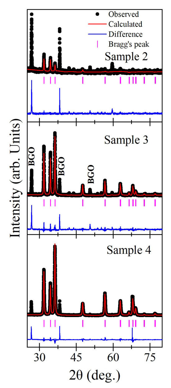
Figure 11.
Observed (black solid circles), calculated (red continuous line), and difference (bottom blue line) profiles obtained from Rietveld refinement of ZnO films in BGO@ZnO heterostructures using P63mc space group. The vertical pink lines indicate the Bragg peak positions.
The refined positional coordinates, unit cell parameters, and agreement factors (χ2 and Rwp) are depicted in Table 2. The Rietveld refinements confirm that the crystal structure remains monophasic hexagonal with the P63mc space group for all prepared materials, with no evidence of secondary phases.
Table 2.
Crystallographic parameters of ZnO films obtained from Rietveld refinement for BGO@ZnO prepared by different methods.
3.4. Optical and Luminescent Properties
Transmission spectra of BGO@ZnO heterostructures with the ZnO films fabricated by different methods are demonstrated in Figure 12a. The heterostructure involving the spin-coated film exhibits significantly better transparency and lower scattering than one with the spray-coated film. The absorption edge of the heterostructures is in the region of about 3.3 eV (Figure 12b), which is close to the known exciton absorption of zinc oxide [32].

Figure 12.
Transmission (a), absorption (b), and photoluminescence at λex = 325 nm excitation (c) of BGO@ZnO heterostructures obtained by the different methods and pristine BGO. The inset in Figure 12a shows the transmission spectrum of a pristine BGO crystal with polished surfaces.
Figure 12c displays the PL spectrum of ZnO films on BGO substrates, as well as pristine BGO excited at 325 nm. The intensity of BGO emission was relatively low because it is poorly excited at this wavelength. Hence, the presented heterostructure emission bands are mainly related to the ZnO films. Our results demonstrated that spectra of all obtained ZnO films contain the two main peaks: the narrow one in the UV region and the broad one centered in the green–orange range. The peaks in the UV range correspond to the radiative recombination of holes in the valence band and electrons in the conduction band, while the broad visible emission band in the ~500–800 nm range is attributed to defect-related luminescence [33,34]. The last one originates from various intrinsic defects in the ZnO structure, such as oxygen vacancies, zinc interstitials, and oxygen interstitials. The position and intensity of the visible emission band vary slightly across samples, indicating differences in defect concentration and film morphology in the different fabrication methods (spin-coating, drop-casting, or spraying). Spin-coated films (Sample 1) show a well-defined UV peak with moderate visible emission, indicating high crystallinity and low defect density. In contrast, drop-casted and sprayed films (Samples 2, 4, and 5) exhibit stronger visible emission bands attributed to higher concentrations of intrinsic defects. Sample 5, prepared by spraying, displays the most intense visible emission and weakest UV peak, likely due to its porous structure and reduced crystallinity. Sample 3 prepared using the spin-coating method with ZnO nanoparticles (Precursor 2), demonstrates the most balanced optical properties among all samples. It exhibits a strong UV peak indicating a high crystallinity, while the visible emission band is moderate, suggesting a lower defect concentration than those in drop-casted and sprayed films. This is also consistent with the lower transmission of the sprayed film on transmission spectra (see Figure 12a). Summarizing, Samples 3 and 5 look like the most suitable candidates for scintillation applications. Sample 3 combines high crystallinity with reduced defect-induced luminescence, which should result in optimized light output and timing resolution required for ultrafast detection. Sample 5 can also be promising as it demonstrates the strongest visible luminescence and second-highest intensity in the UV band. These samples were chosen for CTR measurements.
3.5. CTR Measurements
Table 3 illustrates the main differences between the samples prepared by different techniques. Sample 5, prepared with a spray coating approach, demonstrates a better CTR compared to the reference BGO and Sample 3, obtained by the spin-coating technique.
Table 3.
Coincidence time resolution of the studied samples.
We have verified the samples obtained for possible “shared energy events” [36] from different heterostructure layers. Figure 13 demonstrates only one type of event, preferably produced from the BGO layer. There were no recognizable events from the ZnO layer owing to the small film thickness of 20 μm for stopping 511 keV γ-quanta. Furthermore, the exposition time of 24 h might not be sufficient to recognize those events. We are planning additional experiments with two- or multilayer heterostructures with the increased film thickness and multilayer heterostructures with alternating BGO and ZnO layers to verify this hypothesis. Doping ZnO with Ga, providing higher light yield and extremely fast luminescence decay [1], should also contribute to the enhancement of CTR.

Figure 13.
Events distribution in BGO@ZnO heterostructure.
Figure 14 demonstrates the CTR before and after the time walk correction was added. Additional wrapping with Teflon tape and coupling with optical grease improves light yield and also positively affects the CTR.
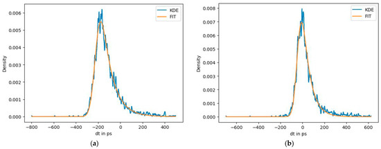
Figure 14.
BGO@ZnO heterostructure before time walk correction with CTR = 202 ± 16 ps (a) and after time–walk correction with CTR = 158 ± 8 ps (b). Reference crystal: LSO:Ce: Ca 3 × 2 × 2 mm3; CTR = 61 ps.
4. Conclusions
BGO@ZnO heterostructures with BGO as a heavy scintillator and ZnO as a fast scintillator were obtained for the first time. The efficiency of different methods of ZnO film deposition on BGO substrates (spin-coating, drop-casting, and spray-coating) was verified using the sol–gel technique. The proposed synthesis methods provide crystalline ZnO films with thicknesses in the range of 6–18 µm on BGO substrates. The nanostructured ZnO films after heat treatment consist of ZnO particles with sizes ranging from 100 to 1000 nm. Among the proposed film preparation techniques, the samples prepared by drop casting and spin coating provided better crystallinity, while the strongest host luminescence in the UV band was observed in the spray-coated sample, evidencing no direct correlation between film crystallinity and luminescence properties. Meanwhile, the best coincidence time resolution of 158 ± 8 ps was registered with the spray-coated BGO@ZnO heterostructure (which provided the strongest visible emission) coupled with silicone to PMMC. The present research showed the feasibility of varying ZnO thickness in the heterostructure, as well as tuning the optical scintillation performance of heterostructures, with the perspective of implementation in detectors for TOF-PET and particle physics. The next steps involve heterostructures with the increased ZnO layer thickness and Ga-doping, as well as creating multilayer heterostructures, which should provide better attenuation of high-energy particles. The ultimate goal is to create 4 × 4 × 20 mm3 pixels capable of substituting single-crystalline BGO or LSO:Ce pixels currently used in positron emission tomography.
Author Contributions
Conceptualization: N.B. and O.S.; methodology: N.B., I.Y., A.P. and O.S.; investigation: N.B., M.J. (Mariusz Jancelewicz), I.I., M.J. (Marcin Jarek), I.Y., A.P., O.V., G.T., C.L., E.A. and O.S.; resources: N.B. and O.S.; writing—original draft: N.B., I.Y. and O.S.; writing—review and editing: N.B., M.J. (Mariusz Jancelewicz), I.I., M.J. (Marcin Jarek), I.Y., A.P., O.V., G.T., C.L., E.A. and O.S.; supervision: N.B. and O.S.; project administration: N.B. and O.S.; funding acquisition: N.B. and O.S. All authors have read and agreed to the published version of the manuscript.
Funding
This research was funded by OPUS project “Heterostructures for ultrafast scintillation detectors” under grant DEC-2022/47/B/ST5/02288 from the National Science Centre (NCN) of Poland.
Data Availability Statement
The data that support the findings of this study are included within the article.
Acknowledgments
Authors acknowledge the Crystal Clear Collaboration in CERN, https://crystalclearcollaboration.web.cern.ch, URL (accessed on 8 September 2025. CERN team acknowledges Horizon Europe ERA Widening Project no. 101078960 “TWISMA”. I.Y., A.P. and O.S. are grateful for the “ENSEMBLE3-Center of Excellence for nanophononics, advanced materials and novel crystal growth-based technologies” project (GA No. MAB/2020/14) carried out under the International Research Agenda programs of the Foundation for Polish Science that are co-financed by the European Union under the European Regional Development Fund and the European Union Horizon 2020 research and innovation program Teaming for Excellence (GA. No. 857543) and the project of the Minister of Science and Higher Education “Support for the activities of Centers of Excellence established in Poland under the Horizon 2020 program” under contract No. MEiN/2023/DIR/3797for supporting this work.
Conflicts of Interest
The authors declare no conflicts of interest.
References
- Lecoq, P.; Morel, C.; Prior, J.O.; Visvikis, D.; Gundacker, S.; Auffray, E.; Križan, P.; Turtos, R.M.; Thers, D.; Charbon, E.; et al. Roadmap toward the 10 ps time-of-flight PET challenge. Phys. Med. Biol. 2020, 65, 21RM01. [Google Scholar] [CrossRef]
- ATLAS Collaboration. Observation of a new particle in the search for the Standard Model Higgs boson with the ATLAS detector at the LHC. Phys. Lett. B 2012, 716, 1–29. [Google Scholar] [CrossRef]
- Lucchini, M.T.; Chung, W.; Eno, S.C.; Lai, Y.; Lucchini, L.; Nguyen, M.; Tully, C.G. New perspectives on segmented crystal calorimeters for future colliders. J. Instrum. 2020, 15, P11005. [Google Scholar] [CrossRef]
- Vinogradov, S. Approximations of coincidence time resolution models of scintillator detectors with leading edge discriminator. Nucl. Instr. Meth. A 2018, 912, 149–153. [Google Scholar] [CrossRef]
- Schaart, D.R. Physics and technology of time-of-flight PET detectors, Physics in Medicine & Biology. Phys. Med. Biol. 2021, 66, 09TR01. [Google Scholar] [CrossRef]
- Derenzo, S.; Boswell, M.; Weber, K. Brennan at the Lawrence Berkeley National Laboratory with Support from the Department of Homeland Security (DHS). Available online: https://scintillator.lbl.gov/ (accessed on 14 September 2025).
- Turtos, R.M.; Gundacker, S.; Auffray, E.; Lecoq, P. Towards a metamaterial approach for fast timing in PET: Experimental proof-of-concept. Phys. Med. Biol. 2019, 64, 185018. [Google Scholar] [CrossRef]
- Turtos, R.M.; Gundacker, S.; Omelkov, S.; Mahler, B.; Khan, A.H.; Saaring, J.; Meng, Z.; Vasil’ev, A.; Dujardin, C.; Kirm, M.; et al. On the use of CdSe scintillating nanoplatelets as time taggers for high-energy gamma detection. Npj 2D Mater. Appl. 2019, 3, 37. [Google Scholar] [CrossRef]
- Pagano, F.; Kratochwil, N.; Salomoni, M.; Pizzichemi, M.; Paganoni, M.; Auffray, E. Advances in heterostructured scintillators: Toward a new generation of detectors for TOF-PET. Phys. Med. Biol. 2022, 67, 135010. [Google Scholar] [CrossRef]
- Shevelev, V.S.; Ishchenko, A.V.; Vanetsev, A.S.; Nagirnyi, V.; Omelkov, S.I. Ultrafast hybrid nanocomposite scintillators: A review. J. Lum. 2022, 242, 118534. [Google Scholar] [CrossRef]
- Chen, Q.; Wu, J.; Ou, X.; Huang, B.; Almutlaq, J.; Zhumekenov, A.A.; Guan, X.; Han, S.; Liang, L.; Yi, Z.; et al. All-inorganic perovskite nanocrystal scintillators. Nature 2018, 561, 88–93. [Google Scholar] [CrossRef]
- Xie, A.; Maddalena, F.; Witkowski, M.E.; Makowski, M.; Mahler, B.; Drozdowski, W.; Springham, V.; Coquet, P.; Dujardin, C.; Birowosuto, M.D.; et al. Library of two-dimensional hybrid lead halide perovskite scintillator, Crystals. Chem. Mater. 2020, 32, 8530–8539. [Google Scholar] [CrossRef]
- Procházková, L.; Gbur, T.; Cuba, V.; Jary, V.; Nikl, M. Fabrication of highly efficient ZnO nanoscintillators. Opt. Mater. 2015, 47, 67–71. [Google Scholar] [CrossRef]
- Koike, K.; Aoki, T.; Fujimoto, R.; Sasa, S.; Yano, M.; Gonda, S.; Ishigami, R.; Kume, K. Radiation hardness of single-crystalline zinc oxide films. Phys. Status Solidi C 2012, 9, 1577–1579. [Google Scholar] [CrossRef]
- Shao, Z.; Cai, Z.; Zhu, H.; Guo, H.; Chen, H.; Yang, F.; Song, X.; Li, J.; Zhang, Q. Influence of neutron/gamma irradiation on damage and scintillation of Ga-doped ZnO thin films. Radiat. Meas. 2023, 160, 106894. [Google Scholar] [CrossRef]
- Dujardin, C.; Auffray, E.; Bourret-Courchesne, E.; Dorenbos, P.; Lecoq, P.; Nikl, M.; Vasil, A.N.; Yoshikawa, A.; Zhu, R.Y. Needs, trends, and advances in inorganic scintillators. IEEE Trans. Nucl. Sci. 2018, 65, 1977–1997. [Google Scholar] [CrossRef]
- Moszynski, M.; Kapusta, M.; Mayhugh, M.; Wolski, D.; Flyckt, S.O. Absolute light output of scintillators. IEEE Trans. Nucl. Sci. 1997, 44, 1052–1061. [Google Scholar] [CrossRef]
- Rogers, E.G.; Birowosuto, M.D.; Maddalena, F.; Dujardin, C.; Pagano, F.; Kratochwil, N.; Auffray, E.; Krause, P.; Bizarri, G. Two-dimensional perovskite functionalized fiber-type heterostructured scintillators. Appl. Phys. Lett. 2023, 122, 081901. [Google Scholar] [CrossRef]
- Taieb, K.; Belkhir, N.; Khennab, A.; Rogers, E.; Giusca, C.; Bizarri, G. High-precision machining behavior of the single crystal scintillator, bismuth germanate (Bi4Ge5O12). Mater. Today Commun. 2025, 46, 112620. [Google Scholar] [CrossRef]
- Anand, V.; Krause, P.; Bansal, B.; Bizarri, G.; Kumar, G.A.; Ranga, V.; Sharma, V. 3D-Printed Plastic Scintillator: A Potential Avenue for Hetero-Structured Radiation Detectors. IEEE Trans. Nucl. Sci. 2025, 72, 2100–2105. [Google Scholar] [CrossRef]
- Orfano, M.; Pagano, F.; Mattei, I.; Cova, F.; Secchi, V.; Bracco, S.; Rogers, E.; Barbieri, L.; Lorenzi, R.; Bizarri, G.; et al. Fast emitting nanocomposites for high-resolution ToF-PET imaging based on multicomponent scintillators. Adv. Mater. Technol. 2024, 9, 2302075. [Google Scholar] [CrossRef]
- Krause, P.; Rogers, E.; Bizarri, G. Advances in design of high-performance heterostructured scintillators for time-of-flight positron emission tomography. Adv. Theory Simul. 2024, 7, 2300425. [Google Scholar] [CrossRef]
- Sans, J.A.; Segura, A.; Mollar, M.; Mari, B. Optical properties of thin films of ZnO prepared by pulsed laser deposition. Thin Solid Films 2004, 251, 453–454. [Google Scholar] [CrossRef]
- Lee, G.H. Optical properties of ZnO thin films on LiNbO3 and LiTaO3 substrates grown by pulsed laser deposition. Solid State Commun. 2003, 128, 351. [Google Scholar] [CrossRef]
- Lee, J.B.; Kwak, S.H.; Kim, H.J. Effects of surface roughness of substrates on the c-axis preferred orientation of ZnO films deposited by r.f. magnetron sputtering. Thin Solid Films 2003, 423, 262–266. [Google Scholar] [CrossRef]
- Cuadra, J.G.; Estrada, A.C.; Oliveira, C.; Abderrahim, L.A.; Porcar, S.; Fraga, D.; Trindade, T.; Seabra, M.P.; Labrincha, J.; Carda, J.B. Functional properties of transparent ZnO thin films synthetized by using spray pyrolysis for environmental and biomedical applications. Ceram. Int. 2023, 49, 32779–32788. [Google Scholar] [CrossRef]
- Paul, G.K.; Bandyopadhyay, S.; Sen, S.K.; Sen, S. Structural, optical and electrical studies on sol–gel deposited Zr doped ZnO films. Mater. Chem. Phys. 2003, 79, 71–75. [Google Scholar] [CrossRef]
- Zhang, W.; Li, P.; Li, Y.; Chen, H.; Wang, X.; Ma, J.; Zhao, X. Structural, optical and electrical properties of sol-gel spin-coated Ga and F Co-doped ZnO films. Thin Solid Films 2022, 746, 139121. [Google Scholar] [CrossRef]
- Beek, W.J.E.; Wienk, M.M.; Kemerink, M.; Yang, X.; Janssen, R.A.J. Hybrid zinc oxide conjugated polymer bulk heterojunction solar cells. J. Phys. Chem. B 2005, 109, 9505–9516. [Google Scholar] [CrossRef]
- Alwan, R.M.; Kadhim, Q.A.; Sahan, K.M.; Ali, R.A.; Mahdi, R.J.; Kassim, N.A.; Jassim, A.N. Synthesis of zinc oxide nanoparticles via sol–gel route and their characterization. J. Nanosci. Nanotechnol. 2015, 5, 1–6. [Google Scholar] [CrossRef]
- Ananthakrishnan, R.; Goswami, K. Deciphering the effect of calcination temperature on crystallinity, morphology, oxygen vacancy and photocatalytic activity of bi-phasic ZnO/ZnCo2O4 heterostructured nanomaterials. Mater. Chem. Phys. 2024, 327, 129792. [Google Scholar] [CrossRef]
- Klingshirn, C.; Priller, H.; Decker, M.; Bruckner, J.; Kalt, H.; Hauschild, R.; Zeller, J.; Waag, A.; Bakin, A.; Wehmann, H.; et al. Excitonic properties of ZnO. Adv. Solid State Phys. 2005, 45, 275–287. [Google Scholar] [CrossRef]
- Kenanakisa, G.; Androulidaki, M.; Koudoumas, E.; Savvakis, C.; Katsarakis, N. Photoluminescence of ZnO nanostructures grown by the aqueous chemical growth technique. Superlattices Microstruct. 2007, 42, 473–478. [Google Scholar] [CrossRef]
- Gruzintsev, A.N.; Dulina, N.A.; Emel, G.A.; Ermolaeva, Y.V.; Kudrenko, E.A.; Tolmachev, A.V. Optical properties of spherical monodisperse Y2O3-ZnO nanoparticles. Phys. Solid State 2012, 54, 2260–2265. [Google Scholar] [CrossRef]
- Mohr, P.; Efthimiou, N.; Pagano, F.; Kratochwil, N.; Pizzichemi, M.; Tsoumpas, C.; Auffray, E.; Ziemonset, K. Image Reconstruction Analysis for Positron Emission Tomography with Heterostructured Scintillators. IEEE Trans. Radiat. Plasma Med. Sci. 2023, 7, 41–51. [Google Scholar] [CrossRef] [PubMed]
- Pagano, F.; Kratochwil, N.; Martinazzoli, L.; Lowis, C.; Paganoni, M.; Pizzichemi, M.; Auffray-Hillemans, E. Modeling scintillation kinetics and coincidence time resolution in heterostructured scintillators. IEEE Trans. Nucl. Sci. 2023, 70, 2630–2637. [Google Scholar] [CrossRef]
Disclaimer/Publisher’s Note: The statements, opinions and data contained in all publications are solely those of the individual author(s) and contributor(s) and not of MDPI and/or the editor(s). MDPI and/or the editor(s) disclaim responsibility for any injury to people or property resulting from any ideas, methods, instructions or products referred to in the content. |
© 2025 by the authors. Licensee MDPI, Basel, Switzerland. This article is an open access article distributed under the terms and conditions of the Creative Commons Attribution (CC BY) license (https://creativecommons.org/licenses/by/4.0/).