Review

Inelastic Electron Tunneling Spectroscopy of Molecular Electronic Junctions: Recent Advances and Applications

Department of Applied Physics, Kyung Hee University, Yongin 17104, Republic of Korea
Crystals 2025, 15(8), 681; https://doi.org/10.3390/cryst15080681 (registering DOI)
Submission received: 2 July 2025 / Revised: 24 July 2025 / Accepted: 25 July 2025 / Published: 26 July 2025
(This article belongs to the Special Issue Advances in Multifunctional Materials and Structures)

Abstract

Inelastic electron tunneling spectroscopy (IETS) has emerged as a powerful vibrational spectroscopy technique for molecular electronic junctions, providing unique insights into molecular vibrations and electron–phonon coupling at the nanoscale. In this review, we present a comprehensive overview of IETS in molecular junctions, tracing its development from foundational principles to the latest advances. We begin with the theoretical background, detailing the mechanisms by which inelastic tunneling processes generate vibrational fingerprints of molecules, and highlighting how IETS complements optical spectroscopies by accessing electrically driven vibrational excitations. We then discuss recent progress in experimental techniques and device architectures that have broadened the applicability of IETS. Central focus is given to emerging applications of IETS over the last decade: molecular sensing (identification of chemical bonds and conformational changes in junctions), thermoelectric energy conversion (probing vibrational contributions to molecular thermopower), molecular switches and functional devices (monitoring bias-driven molecular state changes via vibrational signatures), spintronic molecular junctions (detecting spin excitations and spin–vibration interplay), and advanced data analysis approaches such as machine learning for interpreting complex tunneling spectra. Finally, we discuss current challenges, including sensitivity at room temperature, spectral interpretation, and integration into practical devices. This review aims to serve as a thorough reference for researchers in physics, chemistry, and materials science, consolidating state-of-the-art understanding of IETS in molecular junctions and its growing role in molecular-scale device characterization.

1. Introduction

Molecular electronics envisions using single molecules or self-assembled monolayers as active components in electronic circuits [1,2,3,4,5,6,7,8,9,10,11,12,13,14,15,16,17,18], representing the ultimate limit of device miniaturization. In a typical molecular junction, a molecule is chemically or physically bound between two conductive electrodes, and charge transport through the molecule’s orbitals gives rise to measurable current (I)–voltage (V) characteristics [19,20,21,22,23,24,25]. Studying charge transport at this scale is challenging due to the need to precisely control molecular attachment and contact interfaces [19,24,25]. Over the past two decades, however, significant advances in nanofabrication and measurement techniques have made it possible to form reliable molecular junctions and probe their electrical properties [26,27,28,29,30,31,32]. These efforts have led to demonstrations of molecular diodes, switches, and transistors, highlighting both the promise and the complexity of charge transport through single molecules.
A particularly important breakthrough in the characterization of molecular electronic devices has been the application of inelastic electron tunneling spectroscopy (IETS) as an analytical tool for molecular junctions. IETS is an all-electronic spectroscopic technique that probes the vibrational modes of molecules by measuring the conductance changes caused by inelastic electron–vibration interactions [14,33,34,35]. In IETS, a bias voltage is applied across a tunnel junction and a small AC modulation is superimposed. By using lock-in detection, the second derivative of the IV curve can be recorded as a function of bias [36]. Peaks (or dips) in d2I/dV2 occur at characteristic voltages corresponding to the energies of molecular vibrational modes that electrons can excite during tunneling. Essentially, when a tunneling electron has sufficient energy to excite a particular vibrational mode of the molecule, the tunneling conductance changes, producing a vibrational fingerprint of the molecule in the electrical signal. This capability is invaluable: unlike optical spectroscopies (infrared or Raman) which may require optical selection rules and often probe many molecules at once [37,38], IETS can interrogate a single molecule or a monolayer within a junction, including modes that are IR- or Raman-inactive. Early seminal work by Jaklevic and Lambe in 1966 first demonstrated IETS in metal-oxide tunnel junctions containing molecular impurities [39], revealing that tunneling electrons could indeed excite molecular vibrations and yield spectroscopic information. Subsequently, IETS was developed into a general tool for surface chemistry and thin-film analysis in the 1970s and 1980s and was later adapted to single-molecule junctions in the 2000s as techniques for making nanogaps and break junctions matured [40,41].
IETS has been regarded as a premier analytical tool for investigating nanoscale molecular junctions, which correlates charge transport features with specific molecular vibrational modes. For example, IETS measurements on alkanedithiol self-assembled monolayers (SAMs) between metal electrodes identified C–H and C–C stretching modes, confirming the presence and integrity of the molecular layer and providing evidence of electron–phonon coupling in transport [33,40]. Such vibrational spectroscopy capability is critical for verifying that a molecular junction is indeed formed as intended (as opposed to, say, a direct metal-metal contact or a decomposed molecule) and for understanding how molecular structure influences conductance. Furthermore, IETS offers insights into the electron–vibration interactions that can govern phenomena like electronic heating, current-induced conformational changes, and bond rupture in molecular devices [42,43].
Recently, IETS of molecular junctions has seen several exciting developments. Researchers have explored new junction architectures and electrode materials to improve device stability and yield [5,18,25,26,35,44]. One notable advance is the use of two-dimensional (2D) materials (especially graphene) as electrodes in molecular junctions, mitigating the “filamentary” metal diffusion problems that plagued earlier metal-on-monolayer junction fabrication [26]. This has enabled more robust junctions that consistently exhibit clear IETS signals. Another important methodological breakthrough has been pushing IETS to higher temperatures [45]. Traditionally, IETS experiments are conducted at cryogenic temperatures (often 4–10 K) to sharpen the vibrational features, since thermal broadening at room temperature smears out the small conductance changes [46,47]. In 2021, however, Ngabonziza et al. showed that with careful engineering, it is possible to perform IETS at temperatures well above 300 K [45]. By using a high-quality tunnel barrier and innovative noise reduction, they achieved vibrational resolution up to ~400 K, enabling in situ analysis of, for example, proton diffusion in oxides via IETS peaks corresponding to O–H bond vibrations. This high-temperature IETS capability is a significant step toward practical IETS-based sensors and devices that operate at ambient conditions. Additionally, novel data processing techniques have been introduced, including a numerical derivative algorithm to obtain d2I/dV2 from DC IV data, avoiding the need for lock-in amplifier hardware. This approach, based on Tikhonov regularization, can extract IET spectra from standard IV curves with noise filtering, and showed good agreement with conventional lock-in measurements for both molecular junctions and semiconductor tunnel devices. Such developments simplify IETS measurements and may facilitate integration of IETS detection into broader experimental setups.
With these advancements in place, the applications of IETS have diversified considerably in recent years. In the sections that follow, we describe several key application areas where IETS is playing an enabling role. These mainly include: (1) Molecular sensing and identification, where IETS is used to detect specific molecular bonds or structural changes in nanoscale junctions, ranging from chemical analysis of unknown adsorbates to biomolecular detection in devices. (2) Thermoelectric energy conversion in molecular junctions, where IETS provides insight into vibrational contributions to thermopower and energy dissipation, informing strategies to improve molecular thermoelectric device performance. (3) Spintronic applications, where IETS is combined with magnetic or spin-polarized configurations to probe spin excitations in molecular junctions, offering a window into molecular magnetism and spin–electron interactions at the single-molecule level. (4) Analytical and computational advances, including the use of machine learning and improved theoretical models to analyze IETS data, assign vibrational modes, and even predict IET spectra for complex molecular systems. By addressing each of these topics, we aim to provide a comprehensive and up-to-date picture of how IETS is being utilized.
IETS has evolved from a niche spectroscopy technique into a versatile tool at the intersection of physics, chemistry, and engineering. The ability to probe the vibrations of a molecule as current flows through it is fundamentally enriching our understanding of molecular electronics, and it is opening new avenues for technological innovation (such as quantum-level sensors and novel switching mechanisms) [30,35,48]. The following sections delve into the theoretical foundations of IETS and explore these recent advances in detail.

2. Theoretical Background of IETS in Molecular Junctions

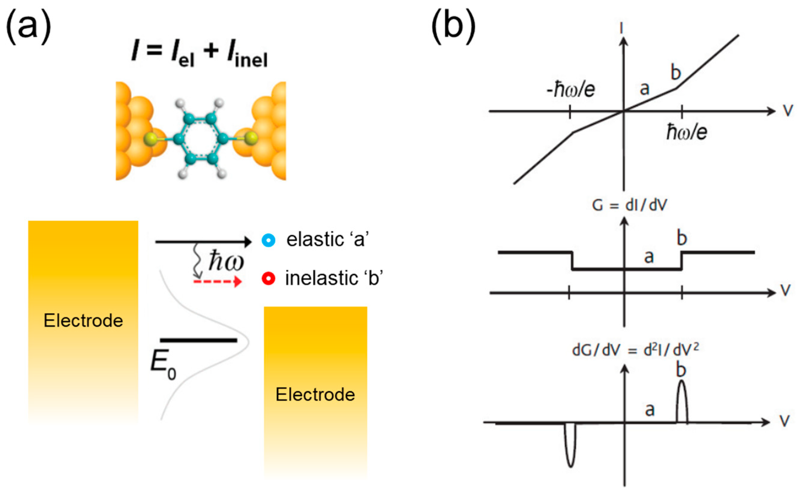
2.1. Basic Principle of IETS

Figure 1a illustrates the principle of IETS in molecular junctions. In a coherent elastic tunneling process (no vibrations excited), an electron’s phase is conserved and it traverses the junction without energy loss (process ‘a’). In contrast, an inelastic tunneling event involves the electron losing a discrete quantum of energy ℏω to excite a vibrational mode of the molecule (or, conversely, gaining energy by absorbing a vibrational quantum if one is thermally excited) (process ‘b’). The occurrence of an inelastic event means that for bias V such that eV = ℏω, a new conductance channel opens (since electrons with higher bias can tunnel both elastically and inelastically) [49,50]. This leads to an increase in the total current. When plotting the first derivative dI/dV (the conductance), this appears as a slight step increase at V = ℏω/e. The effect is more clearly seen in the second derivative d2I/dV2, which will show a peak (for a mode that causes a conductance increase) or a dip (if the inelastic process suppresses conductance) at the corresponding voltage as shown in Figure 1b. The sign of the feature can depend on details like asymmetry of the junction and how the vibrational excitation affects electron tunneling probability [51]. In many molecular junction experiments, peaks are observed on the positive bias side when plotting d2I/dV2, indicating increased conduction due to additional inelastic channels.
Each such spectral feature can be assigned to a particular vibrational mode of the molecule by comparing the voltage position (converted to energy in meV) with the molecule’s known vibrational frequencies from spectroscopy or calculations. For example, C–H stretching modes might appear around 360–370 meV (≈2900 cm−1), while C–C stretches appear at lower energies [52]. The intensity of an IETS peak is related to the coupling strength between the tunneling electron and vibrational mode. Modes that involve motion at the molecule–electrode interface (such as stretching of a metal–sulfur bond in a thiolate junction) often couple strongly and give prominent IETS signals, whereas modes that do not modulate the tunneling current as effectively may produce weak or even unobservable signals [53]. These selection-rule-like tendencies are sometimes referred to as “propensity rules” for IETS [54]. Theoretical studies have shown that highly symmetric vibrations that do not change the overlap or alignment of molecular orbitals during tunneling may have vanishing IET intensity, whereas modes that distort the junction or dipole moment can be more active [51,54].

2.2. Modeling and Calculation

The theoretical modeling of IETS in molecular junctions typically starts from the Landauer–Büttiker formalism for tunneling and introduces electron–vibration (electron–phonon) coupling perturbatively [55]. At low bias, inelastic tunneling can be treated by Fermi’s golden rule: the change in conductance due to a vibration is proportional to the vibration’s occupation and coupling matrix elements between initial and final electronic states [56]. More rigorous approaches use nonequilibrium Green’s function (NEGF) formalisms combined with density functional theory (DFT) to compute IETS spectra of specific molecules [57]. In such calculations, one computes vibrational modes of the molecule (with or without metal atom inclusion for contact modes) and evaluates the changes in electronic transmission when vibrational quanta are emitted or absorbed. DFT-NEGF simulations have been successful in reproducing many experimental IET spectra, allowing researchers to assign peaks to vibrational motions (e.g., differentiating a C–H stretch vs. a N–H bend) [58]. For instance, in a recent study of a graphene–molecule–graphene junction, ab initio calculations of the vibrational modes of the sandwiched molecule were used to label each observed IETS peak with the likely molecular motion (C–H bending, phenyl ring stretch, etc.), and the correspondence was excellent [59]. These assignments build confidence that IETS is truly probing the molecular vibrational degrees of freedom and not artifact signals.

2.3. Experimental Considerations

Obtaining clean IETS spectra requires high sensitivity and careful control of the environment. The signal (d2I/dV2) is typically several orders of magnitude weaker than the conductance itself [46]. Thus, low temperatures (to reduce thermal noise and vibrational broadening) and high measurement stability are important. It is common to use lock-in detection at frequencies in the tens of kHz, with excitation amplitudes of a few mV, to extract the second-harmonic response corresponding to d2I/dV2 [41,47]. The junction must also be stable over the time of signal averaging, which can be challenging for single-molecule junctions that sometimes suffer random switching or drift. Noise reduction is critical. Recent work has even shown that numerical smoothing and regularization can substitute for hardware lock-in [60], obtaining the derivative with minimal noise from a direct IV curve. Another factor is that IETS features have a characteristic lineshape width determined by the intrinsic vibrational lifetime (broadening) and experimental factors [56]. Typically, peaks are Gaussian or Lorentzian with widths of a few mV at cryogenic temperatures; increasing temperature causes significant broadening due to the Fermi distribution in electrodes. For instance, at 77 K, only the very strongest vibrational modes might still be discernible, and by room temperature (~295 K) conventional wisdom held that IETS peaks would wash out entirely. Remarkably, IETS has been demonstrated at 400 K using a proton-conducting oxide tunnel barrier, where highly ordered junctions and careful differential measurements enabled resolution of vibrational features (O–H stretch modes) [60]. This suggests that instrumentation advances—including ultra-low-noise electronics and on-chip amplifiers—could enable IETS operation at practical temperatures for sensing applications.

2.4. Scope of IETS: From Phonon to Spin

While this discussion has focused on vibrational excitations (phonons), it is worth noting that IETS in a broader sense can detect any inelastic channel opening in a tunnel junction. In molecular junctions, the dominant inelastic processes are usually vibrational modes of the molecule. However, if a molecule or device has a spin excitation (e.g., a spin flip or a magnetic anisotropy transition) within the accessible energy range, IETS can in principle detect it similarly. This is the basis of spin-excitation spectroscopy performed with a scanning tunneling microscope on magnetic atoms and molecules [49]. In such experiments, an electron tunneling through a magnetic atom can flip its spin state, leading to a step in conductance at a bias corresponding to the spin splitting energy. The d2I/dV2 spectra in such cases reveal magnetic excitation energies instead of vibrational energies. In Section “Spintronic Applications”, we will discuss examples of this spin-sensitive IETS. Additionally in junctions containing multiple molecules or a molecular layer, collective modes or lattice vibrations of the ensemble could, in principle, contribute to IETS. However, in practice, intramolecular modes are the clearest features observed.
IETS represents a unique form of vibrational spectroscopy embedded within electronic transport measurements. The technique exploits the quantum nature of both tunneling and vibrational excitations to generate molecular signatures. Its sensitivity to local environmental factors—including bonding configurations and mechanical strain—enables IETS to probe molecule–electrode coupling and junction geometry. The following sections demonstrate how these fundamental principles address specific challenges in molecular electronics.

3. Advances in Methods and Materials for IETS

3.1. Mechanically Controlled Break Junctions

One of the most direct ways to create and study a single-molecule junction is by mechanically breaking a tiny metallic wire and trapping a molecule between the freshly formed electrode tips. The mechanically controlled break junction (MCBJ) technique provides sub-ångström precision in adjusting the gap between electrodes by bending a substrate or using a piezoelectric element [61,62,63,64,65,66,67,68,69,70,71,72,73]. This fine control allows one to repeatedly form single-molecule junctions and even manipulate their geometry (e.g., stretching or compressing the molecule) in a stable manner [74]. IETS has been extensively investigated in such MCBJ-created single-molecule junctions [43,49,74]. At low temperatures (typically 2–10 K to reduce thermal broadening), one can obtain vibrational spectra of a single molecule bridging two metal electrodes.
A landmark study by Kim et al. demonstrated the use of IETS to track conformational changes in a single-molecule junction in real time [42]. In this experiment, a hexanedithiol (HDT, HS–(CH2)6–SH) molecule was trapped between gold electrodes. By gently stretching the junction by several ångströms using the MCBJ, the team simultaneously recorded conductance and IETS at each elongation step. The IETS spectrum initially showed vibrational modes consistent with the molecule in an extended all-trans conformation (e.g., C–H stretch, C–C stretch) (Figure 2A). As the junction was pulled, new peaks emerged—notably a mode around 240–250 cm−1 (30 meV) corresponding to the Au–S stretching vibration—and some existing peaks shifted or changed intensity (Figure 2B). These changes were interpreted as signatures of a conformational transition within the molecule: specifically, the HDT molecule transitioning from an initial trans configuration to a gauche configuration under strain. The appearance of the Au–S stretch mode upon stretching indicated that the anchoring geometry was being affected (in this case, possibly the formation of atomic chains on the gold electrodes or a change in the angle of the Au–S bond).
Indeed, the experiments showed that stretching an Au–HDT–Au junction could pull gold atoms out to form a monoatomic chain on the electrodes, whereas doing the same with Pt–HDT–Pt did not form chains (Figure 2C), reflecting the stronger Pt–S bond that breaks the molecule-electrode contact before metal-metal bonds yield. The IETS data, notably the behavior of the metal–sulfur stretch mode, provided direct evidence of these electrode differences: the Au–S vibrational mode remained robust under tension (and did not shift significantly), suggesting the Au–S bond is stronger than the alternative failure mode (Au–Au bonds), whereas in Pt–S junctions the absence of chain formation was consistent with Pt–S bonds breaking first (since Pt–Pt bonds are stronger than Au–Au bonds, but Pt–S is comparatively weaker than Au–S) (Figure 2D). Such detailed information on bond strengths and configurations was extracted from the vibrational spectra, demonstrating the power of IETS in single-molecule mechanics.
Another important application of IETS in single-molecule junctions is to compare different linker chemistries. Molecules can be connected to electrodes via various terminal groups (thiols, amines, phosphines, etc.), which affect both the electronic coupling and mechanical stability of the junction. IETS can probe these differences. For example, Scheer and colleagues measured IETS for alkane molecules terminated with amine linkers versus thiol linkers in otherwise similar junctions [74]. They found that Au–S linked junctions could often be stretched further—even to the point of pulling gold atom chains—whereas Au–NH2 linked junctions would disengage earlier without pulling gold atoms. In the IETS spectra, a vibrational mode corresponding to the Au–N bond was observed and it shifted to lower energy under strain, whereas the Au–S mode in thiol junctions did not shift. This indicates the Au–S bond is mechanically more robust (its vibrational frequency unchanged, implying a strong bond), while the Au–N bond weakens under tension (frequency softening). From such data, the authors concluded quantitatively that the Au–S bond is stronger than the Au–NH2 bond. These molecular-level bond strength comparisons are invaluable for designing junctions—for instance, confirming why thiols make more stable contacts in certain experiments, whereas amines might be preferred for reproducibility but at the cost of weaker binding.

3.2. Scanning Tunneling Microscopy-Based Single-Molecule IETS

While MCBJ experiments focus on a single molecule between two nanoelectrodes, scanning tunneling microscopy (STM) provides another route to single-molecule IETS by positioning a metallic tip over a molecule on a conductive surface. Pioneering STM-IETS studies by Ho and coworkers in the late 1990s demonstrated vibrational spectroscopy of single adsorbed molecules [49]. In such measurements, the STM junction is formed by a metal tip and a metal substrate with the molecule in between (usually adsorbed on the substrate) [62]. Although this setup differs from a two-terminal wired device, it is conceptually similar: the molecule bridges the tip-substrate gap (often through a donor-acceptor bond or even just physisorption), and inelastic tunneling via the molecule’s vibrations can be observed. One advantage of STM-IETS is that it offers atomic-scale spatial resolution—one can obtain a vibrational spectrum at specific locations on a molecule or distinguish different molecules on a surface by their spectra. For example, STM-IETS has been used to map vibrational modes by scanning the tip and recording d2I/dV2 maps, a technique known as inelastic tunneling probe (itProbe) imaging [75]. This method can visualize how vibrations localize within a single molecule or even the “chemical bond” regions between molecules as shown in Figure 3. While STM-IETS typically requires ultra-high vacuum and low temperatures, it has provided remarkable demonstrations, such as resolving the vibrational coupling in a hydrogen molecule between metal tips [76] and detecting spin-flip excitations in magnetic atoms or molecules via inelastic tunneling [77]. These studies broaden the understanding of inelastic tunneling processes and complement the two-terminal junction experiments by offering a microscope’s-eye view of single-molecule spectroscopy.

3.3. Self-Assembled Monolayer Junctions

While single-molecule junction experiments are ideal for probing one molecule in detail, many practical molecular electronic devices and experiments involve self-assembled monolayers (SAMs) or densely packed molecular ensembles between larger-area contacts. These SAM-based junctions typically have 103–106 molecules in parallel, sandwiched between two electrodes (for example, a monolayer on a metal substrate contacted by a top electrode made of metal or liquid metal) [8,16]. IETS has also been extensively applied to such ensemble junctions to investigate their intrinsic charge transport mechanisms and to evaluate their potential for scalable devices [78]. In a SAM junction, the IETS spectrum represents a collective fingerprint of the monolayer. Because many molecules contribute, the signals can be stronger (higher tunneling current through many molecules), but they also represent an average over all molecules in the junction.
One classic example is the IETS study of alkanethiolate SAMs of varying chain lengths. Beebe et al. measured IETS for junctions composed of alkanethiols with different carbon chain lengths (e.g., octanethiol C8, dodecanethiol C12, hexadecanethiol C16) assembled on a metal and contacted with a mercury drop electrode [52]. They observed vibrational peaks corresponding to C–H stretching (~0.36 eV, or ~2900 cm−1), C–H bending (around 0.16–0.17 eV), and C–C skeletal modes (~0.09 eV), among others, in the d2I/dV2 spectra of these SAM junctions. The presence of these modes confirmed that the tunneling current was indeed traversing the molecular layer and not just passing through defects or pinholes (since a pure metallic tunneling path would not show such vibrational features). Furthermore, by comparing intensities and line shapes, researchers could infer information about how molecular length and packing affected the electron–vibration interactions. For instance, longer alkane chains showed slightly attenuated higher-energy modes, consistent with the expectation that tunneling probability decays with length (so vibrational signals from the middle of a long chain are weaker)—a phenomenon related to the exponential length dependence of conductance in the tunneling regime [79,80,81,82,83,84,85,86,87,88].
In addition to the expected vibrational modes of the molecules, SAM junction IETS can reveal subtle effects of environment and defects. In IETS spectra of SAM junctions on gold, a feature around 200–250 cm−1 is often observed [42,52], which can be assigned to the Au–S stretching mode (analogous to single-molecule cases). Its presence and width can indicate the bonding configuration and uniformity of the thiolate headgroups. If some molecules in the SAM adopt different conformations (e.g., due to gauche defects in alkane chains or tilt variations) [42], IETS might show a broadened or split peak for certain modes, or additional modes corresponding to those alternative conformers. For example, Jeong et al. reported that in large-area junctions made by a “direct metal transfer” method (which forms a top electrode without damaging the SAM) [78]. The IETS spectra of alkanedithiols showed all the expected vibrational peaks and allowed assignment of trans versus gauche modes (Figure 4). They also noted that certain vibrational peak intensities varied with bias polarity or device history, suggesting that minor subsets of molecules (perhaps at defect sites or grain boundaries) could have distinct orientations that contribute differently under bias. In general, broadening of vibrational peaks beyond the thermal/modulation broadening can hint at a distribution of environments for that vibrational mode across the many molecules in the junction. For instance, the C–H stretch mode in a well-ordered SAM might appear as a sharp single peak, whereas if half of the molecules are tilted differently (changing their C–H vibrational frequency slightly), the ensemble spectrum could be somewhat broadened or asymmetric [77].

3.4. Two-Dimensional Material Electrodes and Hybrid Junctions

One of the noteworthy developments in molecular junction IETS experiments is the adoption of graphene and other 2D materials as electrode components [25,26,88]. Traditional metal–molecule–metal junctions often suffered from fabrication issues—depositing a top metal electrode onto a molecular layer could result in metal filaments penetrating the layer, shorting out the junction. To avoid this, researchers explored “soft” contacts (e.g., liquid metal Ga–In eutectic or conducting polymers) [89], but these sometimes limited low-temperature performance or stability. Graphene, being a one-atom-thick conductive sheet, offers an ideal solution [90,91,92,93,94,95,96,97]: it can gently contact a molecular layer over a large area without invasive penetration. Moreover, graphene can form π–π interactions or covalent bonds with molecules (especially aromatic molecules), leading to well-defined, reproducible junctions [98,99,100,101,102,103,104,105]. In a recent study, Song et al. constructed graphene/aryl-alkane/graphene vertical junctions and achieved high device yields and stable IETS measurements [59]. The IET spectra showed distinct peaks corresponding to vibrations of the molecular layer, confirming that the molecules remained intact between the graphene electrodes (Figure 5). Notably, the absence of spurious peaks indicated minimal contamination or damage—a testament to the benign nature of graphene top contacts. Graphene’s flexibility is another asset; it can accommodate slight movements of molecules (for instance, due to thermal expansion) without losing contact. Beyond graphene, other 2D materials like h-BN (insulating) or transition metal dichalcogenides have been considered [106,107,108,109,110,111,112,113,114,115,116,117,118,119], either as tunnel barriers or electrode modifiers, to create novel hybrid junctions. The broader category of hybrid molecular junctions also includes setups where a molecule might bridge a metallic and a semiconducting electrode, or a nanoparticle and a surface. Each new electrode material can bring different interfacial chemistry and electronic structure, which in turn can affect IETS. For example, a semiconductor electrode might allow one to tune vibrational features by gating (as vibrational activity can depend on the molecular charge state) [120,121,122,123,124,125,126]. While such experiments are just beginning, the diversification of junction types is expanding the applications of IETS.

3.5. High-Temperature and Low-Noise Techniques

As mentioned, the drive to perform IETS under less restrictive conditions has led to creative approaches. The inherent challenge at high temperatures is that the Fermi–Dirac distributions in the electrodes become smeared, and electrons are thermally excited over a range of energies, which blurs the threshold for inelastic excitations. Ngabonziza et al. addressed this by using a highly symmetric tunnel junction with extremely low zero-bias conductance (indicating a high tunneling barrier), combined with high-resolution measurement of the difference in conductance as a function of bias [45]. By effectively subtracting out the smoothly varying background, they could resolve conductance steps up to 400 K (Figure 6). The demonstration was performed in a solid-state system (oxide proton conductors) relevant to ionics and energy materials, showing that IETS could be used as an analytical tool in those contexts to monitor, for instance, hydrogen motion through solids in real time.
On the electronics side, another advance by Kesarwani et al. was the development of a numerical differentiation algorithm that allows extraction of IET spectra from noisy IV data without requiring a lock-in amplifier [60]. Traditionally, attempting to numerically differentiate IV data to obtain d2I/dV2 is a quick path to amplifying noise. As described in Figure 7, Kesarwani et al. applied Tikhonov regularization (a smoothing technique for solving ill-posed problems) to stabilize the differentiation process [60]. They validated this method on molecular junction data and even on silicon transistor tunneling data, finding that the resulting spectra closely matched those obtained with standard lock-in techniques. This development is promising because it means any DC IV curve stored in a database could be retroactively analyzed for IETS signals, and it reduces the experimental complexity for future studies—one could envision built-in software in semiconductor parameter analyzers that outputs an IET spectrum after measuring an IV characteristic. Together, high-temperature IETS and simplified detection methods pave the way for moving IETS from a specialized low-temperature physics experiment toward a more routine characterization tool in chemistry and materials science.

3.6. Improved Theoretical and Computational Tools

On the theory side, progress has been made in better predicting and understanding IET spectra. For instance, the inclusion of electron correlation effects and more accurate vibrational damping models in calculations has improved agreement with experiments, especially for molecules where mean-field DFT might not capture all physics (e.g., molecules with strong electron–electron interactions or spin states) [58]. New algorithms can calculate not only the energies of vibrational modes but also their IETS intensities by evaluating current–phonon coupling elements from first principles [56]. This has enabled a priori simulations of how an IET spectrum would look for a candidate molecular device, which is extremely useful when screening molecules for certain properties. Additionally, large-scale data approaches have been introduced: researchers have begun constructing databases of vibrational spectra for many molecules (including theoretical IETS and IR/Raman spectra) to apply pattern recognition. With the help of machine learning, one can envision a system where an experimental IETS spectrum is automatically compared against a library to identify the molecule or diagnose the junction configuration. Although this specific application is still nascent, it builds on work in adjacent areas—for example, machine learning models have been used to interpret optical spectra (IR, Raman) and even to discern single-molecule junction conductance traces into different categories of molecular events [127]. These approaches could be extended to IETS data.

4. Applications of IETS in Molecular Junctions

4.1. Molecular Sensors and Chemical Identification

One of the most direct applications of IETS is as a molecular fingerprinting tool, essentially using the junction itself as a sensor to identify molecules or detect changes in molecular structure. Because IETS can provide a vibrational spectrum of molecules confined in a junction, it can be considered an electronic analog to infrared spectroscopy—capable of operating at the nanoscale and even at the single-molecule level. Early on, IETS was employed to confirm the presence of specific functional groups in self-assembled monolayers; for example, observation of a nitro group’s NO2 symmetric stretch in the IET spectrum of a nitrobenzene junction would verify that the molecule is indeed bonded in the junction and remains intact [86]. In recent years, this concept has been extended toward sensing applications [128].
A fascinating idea connecting IETS to sensing is the vibrational theory of olfaction proposed by Turin [129], which posits that our biological nose might distinguish odorant molecules through an inelastic electron tunneling process in receptors, effectively “smelling” via vibrational spectra. While the biological validity remains debated, this theory spurred interest in designing an electronic nose (e-nose) based on IETS that could detect gases by their vibrational signatures. The principle would involve having a tunnel junction containing a binding site for gas molecules; when a target molecule adsorbs, it would introduce new vibrational modes in the junction, detectable as new peaks in the IET spectrum. Bommisetty et al. reported a gas sensor using IETS on functionalized tunnel junctions [130], showing it could differentiate gases like CO2 and CH4 by their distinct spectral peaks. The sensitivity of such IETS-based sensors can be extremely high—potentially down to detecting just a few molecules—because tunneling current is only significantly affected when a molecule is present in the junction. However, achieving this at room temperature with sufficient robustness remains a challenge (cryogenic cooling was often used in experiments to obtain clear spectra).
Another area where IETS serves as a sensor is in monitoring structural changes in molecules under bias. For example, a recent study by Fereiro et al. incorporated a protein (bacteriorhodopsin) into a solid-state junction and used IETS to observe bias-induced changes in the protein’s structure [131]. They detected alterations in certain vibrational peak intensities and frequencies as the bias voltage increased, signaling conformational changes or partial unfolding within the junction (Figure 8). This represents real-time molecular spectroscopy in situ: the ability to apply an electric field and observe the molecule’s response via its vibrational spectrum. Such capability is valuable for molecular diagnostics—one could envision testing the stability of molecular bonds or monitoring the occurrence of a chemical reaction in a junction by observing how an IET spectrum evolves. As another example, if a molecule in a junction is electrochemically active, IETS can sometimes detect the change: different charge states of a molecule may exhibit shifted vibrational frequencies [131]. IETS thus becomes a sensor for the molecule’s electronic state as well.
In the context of biosensing and chemical analysis, IETS has both advantages and disadvantages. On the positive side, it does not require optical access, so it can be integrated on a chip and operate in dark or opaque environments, and it can probe modes that are IR-inactive (due to selection rules). It also naturally lends itself to detecting multiple vibrational features, which aids in identifying unknowns through a “fingerprint matching” approach. On the negative side, IETS traditionally requires low temperatures, which is impractical for everyday sensors, and the requirement of a tunneling junction implies the analyte must be intimately coupled between electrodes, often requiring non-trivial sample preparation. There is ongoing research to overcome these limitations. The high-temperature IETS breakthroughs and the aforementioned numerical methods for analyzing noisy data are steps toward making IETS sensors more viable [45,60]. One could envision arrays of nanoscale junctions, each functionalized to bind a different chemical—a multi-channel IETS e-nose. Indeed, given the interest in quantum and bio-inspired sensing, this approach remains appealing if technical hurdles (stability, fabrication, operating temperature) can be overcome [131]. The use of IETS for molecular sensing is a compelling application that combines chemistry and electronics and recent studies show it can detect not only static molecular fingerprints but also dynamic changes in molecular structure, providing a rich set of information for each molecule or event in the junction.

4.2. Thermoelectric Energy Conversion and Phonon Effects

Molecular junctions have attracted attention as thermoelectric devices, which convert temperature differences into electrical voltage (and vice versa) [132,133,134,135,136,137,138,139]. The performance of a thermoelectric material is quantified by its Seebeck coefficient (thermopower) and figure of merit ZT, which depends on electrical conductance, thermal conductance, and the Seebeck coefficient [140,141,142,143]. Molecules can exhibit very large Seebeck coefficients due to sharp resonances in their electronic structure, and there is hope that by using single molecules or self-assembled monolayers, one might engineer efficient nanoscale thermoelectric generators or coolers [144]. IETS is highly relevant in this context because vibrational (inelastic) processes influence thermoelectric transport in molecular junctions in several ways.
First, inelastic electron scattering from vibrational modes provides a channel for electronic energy to convert into heat (vibrations). This is essentially how electrons dissipate energy in a biased junction: they excite phonons. Such energy dissipation is detrimental to thermoelectric conversion because it represents a loss pathway for what could otherwise be useful electrical energy. Theoretical studies have found that inelastic scattering generally lowers the thermopower of a molecular junction [143]. Intuitively, this occurs because a perfect thermoelectric device would have electrons flowing from hot to cold without losing energy internally; if vibrations capture some energy, the voltage generated per temperature difference decreases [139]. A study on phase-breaking scattering in molecular junctions confirmed that including vibrational scattering in models reduces the Seebeck coefficient, with larger molecules (having more modes) showing more severe reduction [144]. This implies that minimizing electron–phonon coupling is desirable for high ZT—a design principle that can be pursued by, for instance, choosing molecules with specific anchor groups or using deuteration to shift mode frequencies.
On the other hand, IETS provides a tool to actually measure the vibrational spectrum that is responsible for heat flow in the junction [145]. By comparing IET spectra with thermal transport measurements, researchers can identify which vibrational modes are the major heat carriers. For example, if a certain high-frequency mode is strongly excited (visible as a prominent IETS peak) and that mode also carries significant heat (e.g., a stretching mode that couples strongly to thermal reservoirs), one might try to modify the molecule to suppress that mode (perhaps by stiffening it or removing that bond). Thus, IETS can guide molecular design for thermoelectrics by pinpointing “lossy” vibrational channels. Recent literature on molecular thermoelectricity has emphasized understanding vibrational contributions as a key component of improving molecular thermoelectrics [144]. The authors discussed that in purely elastic transport (coherent tunneling with no vibrations), thermopower can be extremely large if a molecular resonance is close to the Fermi level, but in reality, inelastic processes smear out the resonance and also conduct heat directly (lattice thermal conductance) [145]. IETS is essentially the experimental probe of those inelastic processes.
Another aspect is the concept of vibrational engineering to enhance thermoelectric performance [143]. There have been proposals to use inelastic transport in a positive way: for instance, a phenomenon called phonon-assisted tunneling could, under certain circumstances, increase conductance at energies that also enhance the asymmetry needed for thermopower. Also, incorporating weak inelastic channels might filter electrons by energy (only those with sufficient energy to emit a phonon pass through, which can narrow the transmitted energy distribution and potentially increase thermopower). These ideas are still being explored theoretically [144]. From an experimental standpoint, measuring thermopower of molecular junctions while simultaneously performing IETS would be ideal to directly correlate vibrational features with thermoelectric output. There have been experiments measuring Seebeck coefficients in molecular junctions (for example, using EGaIn junctions or scanning probes to create a temperature difference) and, separately, IETS on similar junctions, but combined measurements are challenging [144]. As techniques improve, we may see IETS under thermal bias as a future method—measuring d2I/dV2 with a temperature difference applied could reveal how certain vibrational modes become activated by heat.
IETS contributes to molecular thermoelectric research by: (1) identifying vibrational modes that cause inelastic scattering (hence energy losses) in charge transport, (2) helping to quantify electron–phonon coupling strengths that enter theoretical models of thermopower, and (3) guiding the design of molecular structures that might suppress or alter vibrational properties to improve thermoelectric efficiency. With molecular junction thermoelectric studies now reaching a mature phase (with extensive data on many molecules’ Seebeck coefficients), integrating vibrational spectroscopy into those studies is an important next step, and IETS is the primary tool to accomplish this at the nanoscale.

4.3. Quantum Interference Effects

One of the fascinating quantum phenomena in molecular electronics is quantum interference (QI), which arises when an electron can traverse a molecule via multiple pathways that can interfere constructively or destructively [146]. In certain molecular structures (especially conjugated molecules with multiple connectivity pathways, such as meta-connected benzene rings or cross-conjugated molecules), destructive interference can suppress electron transmission at specific energies, leading to sharp dips in conductance (sometimes even a near-zero transmission node) [146]. Conversely, constructive interference can enhance conductance beyond what a single-pathway model would predict. Quantum interference in single-molecule junctions has been experimentally observed, for example, by comparing conductance of different connectivity isomers [147]. IETS provides an additional window into QI effects because interference not only affects the overall electron transmission but can also modulate how inelastic processes manifest.
Salhani et al. shows the application of IETS to molecular devices where quantum interference phenomena play a crucial role [148]. The experimental setup consists of vertical molecular junctions incorporating anthraquinone (AQ) layers sandwiched between metallic electrodes, where the molecular architecture’s cross-conjugated nature gives rise to destructive quantum interference, leading to pronounced suppression of electrical conductance that amplifies vibrational spectroscopic signatures. The key data presented in Figure 9 illustrates the voltage-dependent behavior of the normalized second derivative measurements, revealing distinct vibrational features across multiple energy domains. Within the lower energy spectrum (below 90 meV), several characteristic vibrational modes emerge, including molecular skeletal distortions near 10 meV, metal-nitrogen bond vibrations approximately at 34 meV, and carbon-nitrogen related modes around 66 meV [148]. The spectroscopic signal intensities in this regime demonstrate exceptional enhancement, reaching values surpassing 5 V−1, which represents a substantial improvement over conventional tunneling spectroscopy measurements. The mid-range energy spectrum (100–250 meV) contains signatures corresponding to various carbon-hydrogen bond deformations occurring at approximately 104 meV and 130 meV, representing different vibrational orientations relative to the molecular plane. Furthermore, collective molecular ring vibrations appear near 170 meV, accompanied by aromatic structural deformations and carbon-oxygen double bond vibrations around 203 meV. At higher energies (250–500 meV), the spectroscopic analysis reveals triple-bonded nitrogen vibrations near 297 meV, hydrogen-related stretching modes around 410 meV, and multiple harmonic overtones associated with various molecular bonds. This investigation yields several important insights for molecular electronics characterization. The quantum interference phenomenon substantially amplifies the detection sensitivity for electron–phonon coupling, especially within the challenging low-energy regime where traditional spectroscopic methods often fail to provide clear signals. The technique successfully probes molecular vibrations across an extended energy window spanning 0–400 meV, surpassing the capabilities of conventional optical spectroscopy methods. Most notably, the approach enables observation of vibrations that remain hidden to infrared techniques, particularly those involving nitrogen-containing molecular bridges and metal-molecule bonding configurations. These findings establish that quantum mechanical interference effects can be purposefully harnessed to enhance spectroscopic characterization of molecular electronic systems. The synergistic combination of quantum interference with tunneling spectroscopy opens new avenues for probing fundamental charge transport processes and electron–phonon interactions in molecular-scale devices, providing essential insights for advancing molecular electronics technology.

4.4. Spintronic Applications of IETS

While IETS traditionally probes vibrational excitations, it can also be applied to magnetic and spin-dependent excitations in molecular junctions—an area overlapping with molecular spintronics. If a molecule has an unpaired spin or a magnetic moment (for example, a spin-crossover complex or a single-molecule magnet), then inelastic tunneling processes can involve spin flips or spin excitations. These will similarly appear as steps in conductance when the bias matches the spin excitation energy, which can be detected by IETS. The key difference is that to observe spin excitations, often a spin-polarized measurement or an external magnetic field is used, because pure spin flips might not strongly affect conductance unless there is spin asymmetry to detect them.
There were STM-based IETS experiments on single magnetic atoms on surfaces that unequivocally showed inelastic spin excitation steps, inaugurating the field of spin excitation spectroscopy with STM [75]. Translating that to molecular junctions (two-terminal devices) took somewhat longer, but now there are examples. For instance, in single-molecule break junctions with magnetic electrodes, researchers have observed changes in IET spectra upon reversing the magnetization alignment of the electrodes—essentially spin-polarized IETS where some vibrational peaks might split or change intensity due to different spin selection rules.
A very recent highlight is the use of IETS to probe quantum spin states in molecular chains on surfaces. Zhao et al. constructed chains of small nanographene molecules (each with spin-1/2) on a gold surface to simulate a one-dimensional antiferromagnetic Heisenberg spin chain [149]. Using a combination of spin-sensitive STM and IETS, they measured the energy spectrum of spin excitations in chains of various lengths. The IETS data revealed, for example, a low-energy “spinon” excitation whose energy gap decreased as the chain length increased, consistent with the expected gapless excitations in an infinite spin-1/2 chain (Figure 10) [149]. This is a remarkable application of IETS: it is being used as a tool for quantum magnetism, verifying theoretical predictions of many-body physics by literally measuring collective spin excitations molecule by molecule. The ability to detect a zero-bias anomaly in IETS corresponding to a spinon mode is something that would not be possible with conventional transport alone. It required identifying subtle features in d2I/dV2 at millivolt energies, made possible by the energy resolution of low-temperature STM-IETS and careful control of the system.
One could use IETS to read out the state of a molecular spin qubit or a molecular memory element. For example, a single-molecule magnet might have two spin states split by magnetic anisotropy. Tunneling electrons can induce transitions between these spin states, and IETS can detect the energy splitting [111]. If that splitting encodes information (say “0” versus “1”), IETS could act as the read-out mechanism. Spin-polarized electrodes could even make the conductance depend on the molecule’s spin state (leading to spin-valve effects combined with vibrational spectroscopy).
Another area is understanding spin–phonon coupling [149]. In molecular magnets, the spin state can couple to molecular vibrations (this is called spin-phonon coupling and is responsible for spin relaxation). IETS could potentially detect this if, for instance, a vibrational peak shifts when the spin state changes. Conversely, a spin excitation might appear as a peak only under certain magnetic field conditions, providing insight into how lattice vibrations and spin states interact.
The application of IETS in spintronics is still a burgeoning field but has shown great promise [150,151,152,153,154,155]: from verifying fundamental spin models to potentially enabling new kinds of molecular spin devices. As techniques improve, we might see IETS being used to characterize spin crossover compounds in junctions (detecting the crossover by its spectroscopic fingerprint) or even to drive and detect spin dynamics (like a form of electrically detected electron spin resonance via inelastic tunneling). This fusion of vibrational spectroscopy with spin physics broadens the horizon of what molecular junction experiments can achieve, connecting molecular electronics with quantum spin science.

4.5. Data Analysis and Machine Learning

With advancing experimental capabilities, both the volume and complexity of data from molecular junction experiments have increased [156,157,158,159,160,161,162,163]. Modern setups can measure thousands of IET spectra (for instance, by repeatedly forming and breaking junctions, each containing a molecule, and recording the spectrum) to build up statistics. Manually analyzing such data or even using straightforward fitting can become a bottleneck. This is where machine learning (ML) and advanced analytical methods are starting to make an impact.
One immediate application is in noise reduction and feature extraction from IET spectra [127]. We discussed earlier the use of regularization algorithms to obtain smooth d2I/dV2 curves. This can be seen as a form of data post-processing that could be further enhanced by ML techniques such as neural network denoising. For instance, one could train a neural network on many examples of theoretical IET spectra (with known peaks) plus added noise, such that the network learns to output a cleaned spectrum highlighting true peaks [127]. This is analogous to what has been done in other spectroscopy fields where ML helps filter noise without losing signal.
Another avenue is automated peak identification and assignment. Normally, identifying peaks in an IET spectrum requires comparison to calculations or known vibrational mode tables. An ML model could be trained on a set of molecules where both the vibrational modes and IET spectral patterns are known, learning the relationship between spectral features and molecular structure. Then for a new spectrum, the model might predict “this looks like a C–H bending mode at 150 meV and a C≡N stretch at 250 meV,” helping the researcher quickly assign peaks [157]. While full generality is difficult, focusing on specific classes of molecules (e.g., alkanes, aromatics, organometallics) could yield useful predictive tools [158]. Already, databases of calculated spectra exist, and combining them with ML has been explored in vibrational spectroscopy more broadly.
A related development is in the analysis of single-molecule break junction data. As described by Komoto et al. machine learning has been successfully applied to thousands of conductance versus distance traces to cluster and identify different molecular binding configurations [127]. This same approach can extend to IETS: for example, if one repeatedly forms a junction with a certain molecule, some junctions might have the molecule bonded in a particular geometry and others in a different geometry, resulting in two families of IET spectra.
It is early days for applying ML specifically to IETS, but given the cross-pollination from other spectroscopies and single-molecule experiments, we anticipate rapid progress. One concrete example already in use is the automated tuning of numerical differentiation parameters mentioned by Kesarwani et al.—they describe an automated scheme to optimize the smoothing parameter for each IV dataset [60]. This is effectively a simple form of machine-assisted optimization. As the community accumulates more IET spectra (especially with the push toward high-throughput or high-temperature measurements that may generate more data per experiment), the role of ML will naturally grow. The payoff will be faster analysis, extraction of subtle correlations (perhaps linking a combination of peak intensities to, say, junction conductance or specific molecule-metal contacts), and possibly the discovery of patterns that humans might overlook when sifting through spectral data manually.
While machine learning has not yet become a standard tool in every molecular IETS study, it is poised to become one. Its applications range from improving data quality to interpreting results in terms of molecular structure. The combination of rich spectral data with advanced analysis will further empower IETS as a technique, ensuring that researchers can fully leverage the information content of these measurements.

5. Conclusions and Perspectives

IETS of molecular electronic junctions has progressed from scientific curiosity into a mature and multifaceted tool for nanoscale science [164,165,166,167,168,169,170]. Over the course of this review, we have seen how the fundamental principle of inelastic tunneling—electrons exciting molecular vibrations and other quanta—underpins a spectroscopy method that yields a vibrational fingerprint of molecules in situ. By measuring the second derivative of the IV characteristics, researchers can glean detailed information about which bonds and modes are present in a molecular junction, confirming molecular identity and providing insight into electron–phonon coupling. The Introduction and Theoretical Background sections highlighted that the in situ vibrational spectroscopy capability is what makes IETS uniquely powerful: it directly connects the electrical behavior of a device to the molecular structure and dynamics within it.
In recent years, the scope of IETS has significantly broadened [171,172,173,174]. Advances in materials and methods—such as the use of graphene electrodes for creating robust molecular junctions and new techniques enabling room-temperature IETS measurements—have overcome many experimental limitations, paving the way for IETS to be performed in more varied and practical settings. Simplified measurement schemes (such as numerical derivative processing) and integration with other platforms mean that IETS can now be applied to systems ranging from single-molecule devices to solid-state electrolytes and thin films, well beyond the low-temperature ultrahigh-vacuum setups of its early years.
Concomitantly, we have seen IETS find applications across a spectrum of cutting-edge research areas. In molecular sensing, IETS can serve as an electronic “nose,” capable of detecting molecules by their vibrational signatures and even observing structural changes in real time. In the realm of thermoelectric energy conversion, IETS provides crucial understanding of how vibrational scattering affects molecular thermopower, guiding efforts to design better thermoelectric materials at the molecular scale. For molecular switches and devices, IETS acts as a diagnostic that can verify the operational state of a molecule (e.g., which conformation or charge state it is in) by revealing the corresponding vibrational spectrum, thereby linking function to structure. In spintronics, IETS has enabled the detection of spin excitations and magnons in molecular systems, merging molecular electronics with quantum spin physics and demonstrating the versatility of inelastic tunneling spectroscopy in probing not just vibrations but any excitation within a junction. Finally, we discussed how data analysis and machine learning are beginning to enhance IETS experiments, improving noise filtering and allowing automated interpretation of complex spectral data—developments that will be increasingly important as datasets grow in size and complexity.
Looking forward, several challenges and opportunities can be identified for IETS research and its application in technology:
Room-Temperature and Real-Time IETS: A major challenge remains the extension of IETS to truly ambient conditions. While progress has been made up to ~400 K in specialized systems, typical molecular junction experiments at room temperature still struggle to resolve vibrational features. Overcoming this will likely require a combination of improved instrumentation (low-noise electronics, perhaps on-chip amplification or AC excitation methods), smarter data processing (as provided by machine learning denoising), and junction engineering (to enhance IETS signals, e.g., incorporating resonant tunneling elements that amplify inelastic effects). Success in this area would open the door to practical IETS-based sensors operating at room temperature—for example, handheld electronic nose devices for medical diagnostics or environmental monitoring, directly analyzing chemical composition via vibrational fingerprints. This is an enticing prospect for the translational impact of IETS.
Integration with Device Architectures: To move IETS from laboratory measurements to integrated technology, one can envision on-chip tunnel junction arrays or IETS-active transistors. One opportunity is to integrate a molecular junction (or a thin-film junction) that produces IET spectra into a CMOS-compatible platform [175,176,177,178,179,180,181,182,183,184]. There have been initial attempts using metal-oxide-semiconductor (MOS) structures to perform IETS on gate dielectrics, suggesting that one might build IETS functionality into a transistor gate stack (where the insulator and a trapped molecule produce inelastic signals). If each transistor could “sense” molecules by IETS, that would be transformative for sensor networks on chips. Achieving this requires addressing scaling issues (how to make thousands of identical junctions) and readout speed (IETS is traditionally slow due to averaging, but perhaps multiplexing many junctions could alleviate that). The hybrid molecular–solid-state junction approach, such as large-area molecular ensemble junctions or nanopore-trapped molecules, might provide a bridge between single-molecule IETS and device-level reproducibility.
Deeper Theoretical Understanding: On the fundamental side, as experiments push into new regimes (high bias, high fields, strong coupling), our theoretical models of IETS will be tested and need refinement. In particular, nonlinear and higher-order effects in IETS could contain more information than we currently extract. For instance, at very high bias, multiple vibrational quanta might be excited (overtones or combination bands)—there is evidence of overtone modes in some IET spectra. Understanding and utilizing these could enhance the information content. Also, in devices out of equilibrium, vibrational populations might deviate from thermal equilibrium (electrons might pump certain modes), leading to non-equilibrium vibrational spectroscopy via IETS. Theoretical frameworks that include these effects (perhaps involving molecular dynamics coupled with electron transport) will be important for interpreting next-generation experiments.
Multifunctional and Coupled Excitations: Future IETS studies may explore coupled excitations—for example, vibronic interactions (where an electronic resonance and a vibrational excitation interplay), or spin-phonon coupling as noted. A challenge and opportunity is to use IETS to study energy conversion at the single-molecule level: how an electron’s energy can convert to a vibrational excitation and then perhaps to a photon (if a molecule is light-emitting) or to a spin flip. These multimodal energy conversions are at the heart of molecular machines and sensors. IETS could be part of a combined spectroscopic approach (for example, simultaneously measuring IETS and light emission from a biased junction to correlate vibrational excitation with photon emission events).
Machine Learning and Automated Discovery: As machine learning techniques mature, we anticipate autonomous experimentation in IETS. An AI system could adjust bias ranges, temperatures, or molecular candidates in real-time to optimize spectral data or discover new phenomena. For example, it could learn that a certain molecule shows an unusual peak at a certain bias and then automatically try a series of similar molecules to see if the peak shifts or disappears, thus mapping a trend without full manual intervention. Such approaches could greatly accelerate materials discovery for molecular electronics—essentially using IETS as the feedback signal in a closed-loop discovery algorithm.
In conclusion, the trajectory of inelastic electron tunneling spectroscopy in molecular junctions is strongly upward. It has proven its worth in fundamental research—solving mysteries of molecular conduction and revealing the intimate dance between electrons and nuclei at the nanoscale—and it is steadily moving toward practical applicability in sensing and materials characterization. The challenges that remain are, in many ways, opportunities that define an exciting research agenda, pushing the limits of sensitivity, integrating with complex systems, and harnessing new analytical tools to fully exploit the wealth of information IETS can provide. Given the ingenuity and interdisciplinary collaboration apparent in the advances of the last decade, there is every reason to be optimistic that IETS will continue to thrive and contribute significantly to nanoscience and nanotechnology in the years to come.

Funding

This work was supported by Kyung Hee University (KHU-20250584).

Data Availability Statement

Data is contained within the article.

Conflicts of Interest

The author declares no conflicts of interest.

References

  1. Aviram, A.; Ratner, M.A. Molecular rectifiers. Chem. Phys. Lett. 1974, 29, 277–283. [Google Scholar] [CrossRef]
  2. Tao, N.J. Electron transport in molecular junctions. Nat. Nanotechnol. 2006, 1, 173–181. [Google Scholar] [CrossRef]
  3. Al-Owaedi, O.A.; Najeeb, H.N.; Aldulaimi, A.K.O.; Alwan, N.H.; Ali, M.S.; Dwech, M.H.; AL-Da’amy, M.A. Thermoelectric signature of d-orbitals in tripod-based molecular junctions. Mater. Adv. 2024, 5, 9781–9791. [Google Scholar] [CrossRef]
  4. Song, H.; Reed, M.A.; Lee, T. Single molecule electronic device. Adv. Mat. 2011, 23, 1583–1608. [Google Scholar] [CrossRef]
  5. Yuan, M.; Qiu, Y.; Gao, H.; Feng, J.; Jiang, L.; Wu, Y. Molecular electronics: From nanostructure assembly to device integration. J. Am. Chem. Soc. 2024, 146, 7885–7904. [Google Scholar] [CrossRef]
  6. Moreno-Pineda, E.; Wernsdorfer, W. Measuring molecular magnets for quantum technologies. Nat. Rev. Phys. 2021, 3, 645–659. [Google Scholar] [CrossRef]
  7. Yu, C.J.; Von Kugelgen, S.; Laorenza, D.W.; Freedman, D.E. A molecular approach to quantum sensing. ACS Cent. Sci. 2021, 7, 712–723. [Google Scholar] [CrossRef]
  8. Xiang, D.; Wang, X.; Jia, C.; Lee, T.; Guo, X. Molecular-Scale Electronics: From Concept to Function. Chem. Rev. 2016, 116, 4318–4440. [Google Scholar] [CrossRef]
  9. McCreery, R.L.; Yan, H.; Bergren, A.J. A Critical Perspective on Molecular Electronic Junctions: There Is Plenty of Room in the Middle. Phys. Chem. Chem. Phys. 2013, 15, 1065–1081. [Google Scholar] [CrossRef]
  10. Chen, H.; Stoddart, J.F. From Molecular to Supramolecular Electronics. Nat. Rev. Mater. 2021, 6, 804–828. [Google Scholar] [CrossRef]
  11. Perrin, M.L.; Burzurı, E.; van der Zant, H.S.J. Single-Molecule Transistors. Chem. Soc. Rev. 2015, 44, 902–919. [Google Scholar] [CrossRef]
  12. Ratner, M. A Brief History of Molecular Electronics. Nat. Nanotechnol. 2013, 8, 378–381. [Google Scholar] [CrossRef]
  13. Cuevas, J.C.; Scheer, E. Molecular Electronics: An Introduction to Theory and Experiment; World Scientific: Singapore, 2009. [Google Scholar]
  14. Song, H.; Kim, Y.; Jang, Y.H.; Jeong, H.; Reed, M.A.; Lee, T. Observation of molecular orbital gating. Nature 2009, 462, 1039–1043. [Google Scholar] [CrossRef]
  15. Aradhya, S.V.; Venkataraman, L. Single-molecule junctions beyond electronic transport. Nat. Nanotechnol. 2013, 8, 399–410. [Google Scholar] [CrossRef]
  16. Vilan, A.; Aswal, D.; Cahen, D. Large-Area, Ensemble Molecular Electronics: Motivation and Challenges. Chem. Rev. 2017, 117, 4248–4286. [Google Scholar] [CrossRef]
  17. Reed, M.A.; Zhou, C.; Muller, C.J.; Burgin, T.P.; Tour, J.M. Conductance of a molecular junction. Science 1997, 278, 252–254. [Google Scholar] [CrossRef]
  18. Li, L.; Low, J.Z.; Wilhelm, J.; Liao, G.; Gunasekaran, S.; Prindle, C.R.; Starr, R.L.; Golze, D.; Nuckolls, C.; Steigerwald, M.L.; et al. Highly conducting single-molecule topological insulators based on mono- and di-radical cations. Nat. Chem. 2022, 14, 1061–1067. [Google Scholar] [CrossRef]
  19. Haiss, W.; Nichols, R.J.; van Zalinge, H.; Higgins, S.J.; Bethell, D.; Schiffrin, D.J. Measurement of single molecule conductivity using the spontaneous formation of molecular wires. Phys. Chem. Chem. Phys. 2004, 6, 4330–4337. [Google Scholar] [CrossRef]
  20. Wang, W.; Lee, T.; Reed, M.A. Mechanism of electron conduction in self-assembled alkanethiol monolayer devices. Phys. Rev. B 2003, 68, 035416. [Google Scholar] [CrossRef]
  21. Hines, T.; Diez-Perez, I.; Hihath, J.; Liu, H.; Wang, Z.S.; Zhao, J.; Zhou, G.; Müllen, K.; Tao, N. Transition from Tunneling to Hopping in Single Molecular Junctions by Measuring Length and Temperature Dependence. J. Am. Chem. Soc. 2010, 132, 11658. [Google Scholar] [CrossRef]
  22. Leary, E.; Limburg, B.; Alanazy, A.; Sangtarash, S.; Grace, I.; Swada, K.; Esdaile, L.J.; Noori, M.; Teresa Gonzalez, M.; Rubio-Bollinger, G.; et al. Bias-Driven Conductance Increase with Length in Porphyrin Tapes. J. Am. Chem. Soc. 2018, 140, 12877. [Google Scholar] [CrossRef]
  23. Brooke, C.; Vezzoli, A.; Higgins, S.J.; Zotti, L.A.; Palacios, J.J.; Nichols, R.J. Resonant transport and electrostatic effects in single-molecule electrical junctions. Phys. Rev. B 2015, 91, 195438. [Google Scholar] [CrossRef]
  24. Evers, F.; Korytar, R.; Tewari, S.; van Ruitenbeek, J.M. Advances and challenges in single-molecule electron transport. Rev. Mod. Phys. 2020, 92, 035001. [Google Scholar] [CrossRef]
  25. He, C.; Zhang, Q.; Fan, Y.; Zhao, C.Z.; Zhao, C.; Ye, J.; Dappe, Y.J.; Nichols, R.J.; Yang, L. Effect of Asymmetric Anchoring Groups on Electronic Transport in Hybrid Metal/Molecule/Graphene Single Molecule Junctions. Chem. Phys. Chem. 2019, 20, 1830. [Google Scholar] [CrossRef]
  26. Tao, S.; Zhang, Q.; He, C.; Lin, X.; Xie, R.; Zhao, C.Z.; Zhao, C.; Smogunov, A.; Dappe, Y.J.; Nichols, R.J.; et al. Graphene-Contacted Single Molecular Junctions with Conjugated Molecular Wires. ACS Appl. Nano Mater. 2019, 2, 12. [Google Scholar] [CrossRef]
  27. Baghernejad, M.; Van Dyck, C.; Bergfield, J.; Levine, D.R.; Gubicza, A.; Tovar, J.D.; Calame, M.; Broekmann, P.; Hong, W. Quantum interference enhanced chemical responsivity in single-molecule dithienoborepin junctions. Chem. Eur. J. 2019, 25, 15141–15146. [Google Scholar] [CrossRef]
  28. Li, Y.H.; Artes, J.M.; Demir, B.; Gokce, S.; Mohammad, H.M.; Alangari, M.; Anantram, M.P.; Oren, E.E.; Hihath, J. Detection and identification of genetic material via single-molecule conductance. Nat. Nanotechnol. 2018, 13, 1167–1173. [Google Scholar] [CrossRef]
  29. Li, X.M.; Wang, Y.H.; Seng, J.W.; Zheng, J.F.; Cao, R.; Shao, Y.; Chen, J.Z.; Li, J.F.; Zhou, X.S.; Mao, B.W. Z-Piezo pulse-modulated STM Break Junction: Toward single-molecule rectifiers with dissimilar metal electrodes. ACS Appl. Mater. Interfaces 2021, 13, 8656–8663. [Google Scholar] [CrossRef]
  30. Wang, Y.H.; Huang, H.; Yu, Z.; Zheng, J.F.; Shao, Y.; Zhou, X.S.; Chen, J.Z.; Li, J.F. Modulating electron transport through single-molecule junctions by heteroatom substitution. J. Mater. Chem. C 2020, 8, 6826–6831. [Google Scholar] [CrossRef]
  31. Kay, N.J.; Higgins, S.J.; Jeppesen, J.O.; Leary, E.; Lycoops, J.; Ulstrup, J.; Nichols, R.J. Single-molecule electrochemical gating in ionic liquids. J. Am. Chem. Soc. 2012, 134, 16817–16826. [Google Scholar] [CrossRef]
  32. Seng, J.W.; Tong, L.; Peng, X.Q.; Chang, W.Y.; Xie, W.; Wang, Y.H.; Zheng, J.F.; Shao, Y.; Chen, J.Z.; Jin, S.; et al. Influence of a coordinated metal center on charge transport through a Series of porphyrin molecular junctions. J. Phys. Chem. C 2022, 126, 1168–1175. [Google Scholar] [CrossRef]
  33. Wang, W.; Lee, T.; Kretzschmar, I.; Reed, M.A. Inelastic electron tunneling spectroscopy of an alkanedithiol self-assembled monolayer. Nano Lett. 2004, 4, 643–646. [Google Scholar] [CrossRef]
  34. Reed, M.A. Inelastic electron tunneling spectroscopy. Mater. Today 2008, 11, 46–50. [Google Scholar] [CrossRef]
  35. Cao, Y.; Austin, D.; Switzer, E.D.; Rowen, J.F.; Sander, W.; Rahman, T.S.; Morgenstern, K. Inelastic electron tunneling spectroscopy as a probe of electronic coupling at a molecule-metal interface. Phys. Rev. B 2025, 111, 115426. [Google Scholar] [CrossRef]
  36. Jaklevic, R.C.; Gaerttner, M.R. Inelastic electron tunneling spectroscopy. experiments on external doping of tunnel junctions by an infusion technique. Appl. Surf. Sci. 1978, 1, 479–502. [Google Scholar] [CrossRef]
  37. Kushmerick, J.G.; Lazorcik, J.; Patterson, C.H.; Shashidhar, R.; Seferos, D.S.; Bazan, G.C. Vibronic contributions to charge transport across molecular junctions. Nano Lett. 2004, 4, 639–642. [Google Scholar] [CrossRef]
  38. Lambe, J.; Jaklevic, R.C. Molecular vibration spectra by inelastic electron tunneling. Phys. Rev. 1968, 165, 821. [Google Scholar] [CrossRef]
  39. Jaklevic, R.C.; Lambe, J. Molecular vibration spectra by electron tunneling. Phys. Rev. Lett. 1966, 17, 1139. [Google Scholar] [CrossRef]
  40. Song, H.; Kim, Y.; Ku, J.; Jang, Y.H.; Jeong, H.; Lee, T. Vibrational spectra of metal-molecule-metal junctions in electromigrated nanogap electrodes by inelastic electron tunneling. Appl. Phys. Lett. 2009, 94, 103110. [Google Scholar] [CrossRef]
  41. Tal, O.; Krieger, M.; Leerink, B.; van Ruitenbeek, J.M. Electron-vibration interaction in single-molecule junctions: From contact to tunneling regimes. Phys. Rev. Lett. 2008, 100, 196804. [Google Scholar] [CrossRef]
  42. Kim, Y.; Song, H.; Strigl, F.; Pernau, H.F.; Lee, T.; Scheer, E. Conductance and vibrational states of single-molecule junctions controlled by mechanical stretching and material variation. Phys. Rev. Lett. 2011, 106, 196804. [Google Scholar] [CrossRef]
  43. Kim, Y.; Hellmuth, T.J.; Burkle, M.; Pauly, F.; Scheer, E. Characteristics of amine-ended and thiol-ended alkane single-molecule junctions revealed by inelastic electron tunneling spectroscopy. ACS Nano 2011, 5, 4104–4111. [Google Scholar] [CrossRef]
  44. Vuillaume, D. Molecular Electronics: From Single-Molecule to Large-Area Devices. Chempluschem 2019, 84, 1215–1221. [Google Scholar] [CrossRef]
  45. Ngabonziza, P.; Wang, Y.; van Aken, P.A.; Maier, J.; Mannhart, J. Inelastic electron tunneling spectroscopy at high-temperatures. Adv. Mater. 2021, 33, 2007299. [Google Scholar] [CrossRef]
  46. Hansma, P.K. Inelastic electron tunneling. Phys. Rep. 1977, 30, 145–206. [Google Scholar] [CrossRef]
  47. Horiuchi, T.; Ebisawa, F.; Tabei, H. New inelastic electron tunneling spectrometer with an absolute peak intensity. Rev. Sci. Instrum. 1989, 60, 993–996. [Google Scholar] [CrossRef]
  48. Troisi, A.; Beebe, J.M.; Picraux, L.B.; van Zee, R.D.; Stewart, D.R.; Ratner, M.A.; Kushmerick, J.G. Tracing electronic pathways in molecules by using inelastic tunneling spectroscopy. Proc. Natl. Acad. Sci. USA 2007, 104, 14255–14259. [Google Scholar] [CrossRef]
  49. Stipe, B.C.; Rezaei, M.A.; Ho, W. Single-molecule vibrational spectroscopy and microscopy. Science 1998, 280, 1732–1735. [Google Scholar] [CrossRef]
  50. Kushmerick, J.G.; Holt, D.B.; Yang, J.C.; Naciri, J.; Moore, M.H.; Shashidhar, R. Metal-molecule contacts and charge transport across monomolecular layers:measurement and theory. Phys. Rev. Lett. 2002, 89, 086802. [Google Scholar] [CrossRef]
  51. Troisi, A.; Ratner, M.A.; Nitzan, A. Vibronic effects in off-resonant molecular wire conduction. J. Chem. Phys. 2003, 118, 6072–6082. [Google Scholar] [CrossRef]
  52. Beebe, J.M.; Moore, H.J.; Lee, T.R.; Kushmerick, J.G. Vibronic coupling in semifluorinated alkanethiol junctions: Implications for selection rules in inelastic electron tunneling spectroscopy. Nano Lett. 2007, 7, 1364–1368. [Google Scholar] [CrossRef]
  53. Lauhon, L.J.; Ho, W. Effects of temperature and other experimental variables on single molecule vibrational spectroscopy with the scanning tunneling microscope. Rev. Sci. Instrum. 2001, 72, 216–223. [Google Scholar] [CrossRef]
  54. Galperin, M.; Ratner, M.A.; Nitzan, A.; Troisi, A. Nuclear coupling and polarization in molecular transport junctions: Beyond tunneling to function. Science 2008, 319, 1056–1060. [Google Scholar] [CrossRef]
  55. Paulsson, M.; Frederiksen, T.; Ueba, H.; Lorente, N.; Brandbyge, M. Unified description of inelastic propensity rules for electron transport through nanoscale junctions. Phys. Rev. Lett. 2008, 100, 226604. [Google Scholar] [CrossRef]
  56. Galperin, M.; Ratner, M.A.; Nitzan, A. Inelastic electron tunneling spectroscopy in molecular junctions: Peaks and dips. J. Chem. Phys. 2004, 121, 11965–11979. [Google Scholar] [CrossRef]
  57. Persson, B.N.J.; Baratoff, A. Inelastic electron-tunneling from a metal tip—The contribution from resonant processes. Phys. Rev. Lett. 1987, 59, 339–342. [Google Scholar] [CrossRef]
  58. Kirtley, J.; Scalapino, D.J.; Hansma, P.K. Theory of vibrational mode intensities in inelastic electron tunneling spectroscopy. Phys. Rev. B 1976, 14, 3177. [Google Scholar] [CrossRef]
  59. Song, H. Inelastic Electron Tunneling Spectroscopy of Aryl Alkane Molecular Junction Devices with Graphene Electrodes. Crystals 2025, 15, 433. [Google Scholar] [CrossRef]
  60. Kesarwani, S.; Misra, S.; Saha, D.; Della Rocca, M.L.; Roy, I.; Ganguly, S.; Mahajan, A. Simplified inelastic electron tunneling spectroscopy based on low-noise derivatives. Sci. Rep. 2022, 12, 19216. [Google Scholar] [CrossRef]
  61. Singh, A.K.; Martin, K.; Mastropasqua Talamo, M.; Houssin, A.; Vanthuyne, N.; Avarvari, N.; Tal, O. Single-molecule junctions map the interplay between electrons and chirality. Nat. Commun. 2025, 16, 1759. [Google Scholar] [CrossRef]
  62. Agrait, N.; Yeyati, A.L.; van Ruitenbeek, J.M. Quantum properties of atomic-sized conductors. Phys. Rep. 2003, 377, 81–279. [Google Scholar] [CrossRef]
  63. Gooding, J.J.; Gaus, K. Single-molecule sensors: Challenges and opportunities for quantitative analysis. Angew. Chem. Int. Ed. 2016, 55, 11354–11366. [Google Scholar] [CrossRef]
  64. Holzmeister, P.; Acuna, G.P.; Grohmann, D.; Tinnefeld, P. Breaking the concentration limit of optical single-molecule detection. Chem. Soc. Rev. 2014, 43, 1014–1028. [Google Scholar] [CrossRef]
  65. Venkataraman, L.; Klare, J.E.; Nuckolls, C.; Hybertsen, M.S.; Steigerwald, M.L. Dependence of single-molecule junction conductance on molecular conformation. Nature 2006, 442, 904–907. [Google Scholar] [CrossRef]
  66. Tam, E.S.; Parks, J.J.; Shum, W.W.; Zhong, Y.W.; Santiago-Berríos, M.E.B.; Zheng, X.; Yang, W.; Chan, G.K.L.; Abruña, H.D.; Ralph, D.C. Single-molecule conductance of pyridine-terminated dithienylethene switch molecules. ACS Nano 2011, 5, 5115–5123. [Google Scholar] [CrossRef]
  67. Nichols, R.J.; Higgins, S.J. Single molecule nanoelectrochemistry in electrical junctions. Acc. Chem. Res. 2016, 49, 2640–2648. [Google Scholar] [CrossRef]
  68. Xiao, B.; Liang, F.; Liu, S.; Im, J.; Li, Y.; Liu, J.; Zhang, B.; Zhou, J.; He, J.; Chang, S. Cucurbituril mediated single molecule detection and identification via recognition tunneling. Nanotechnology 2018, 29, 365501. [Google Scholar] [CrossRef]
  69. Ahn, S.; Aradhya, S.V.; Klausen, R.S.; Capozzi, B.; Roy, X.; Steigerwald, M.L.; Nuckolls, C.; Venkataraman, L. Electronic transport and mechanical stability of carboxyl linked single-molecule junctions. Phys. Chem. Chem. Phys. 2012, 14, 13841–13845. [Google Scholar] [CrossRef]
  70. Xiao, X.; Xu, B.; Tao, N. Changes in the conductance of single peptide molecules upon metal-ion binding. Angew. Chem. Int. Ed. 2004, 43, 6148–6152. [Google Scholar] [CrossRef]
  71. Kiguchi, M.; Ohto, T.; Fujii, S.; Sugiyasu, K.; Nakajima, S.; Takeuchi, M.; Nakamura, H. Single Molecular Resistive Switch Obtained via Sliding Multiple Anchoring Points and Varying Effective Wire Length. J. Am. Chem. Soc. 2014, 136, 7327–7332. [Google Scholar] [CrossRef]
  72. Su, T.A.; Li, H.; Steigerwald, M.L.; Venkataraman, L.; Nuckolls, C. Stereoelectronic switching in single-molecule junctions. Nat. Chem. 2015, 7, 215–220. [Google Scholar] [CrossRef]
  73. Kiguchi, M.; Nakashima, S.; Tada, T.; Watanabe, S.; Tsuda, S.; Tsuji, Y.; Terao, J. Single-Molecule Conductance of π-Conjugated Rotaxane: New Method for Measuring Stipulated Electric Conductance of π-Conjugated Molecular Wire Using STM Break Junction. Small 2012, 8, 726–730. [Google Scholar] [CrossRef]
  74. Kim, Y.; Pietsch, T.; Erbe, A.; Belzig, W.; Scheer, E. Benzenedithiol: A Broad-Range Single-Channel Molecular Conductor. Nano Lett. 2011, 11, 3734–3738. [Google Scholar] [CrossRef]
  75. Chiang, C.L.; Xu, C.; Han, Z.M.; Ho, W. Real-space imaging of molecular structure and chemical bonding by single-molecule inelastic tunneling probe. Science 2014, 344, 885–888. [Google Scholar] [CrossRef]
  76. Smit, R.H.M.; Noat, Y.; Untiedt, C.; Lang, N.D.; van Hemert, M.C.; van Ruitenbeek, J.M. Measurement of the conductance of a hydrogen molecule. Nature 2002, 419, 906–909. [Google Scholar] [CrossRef]
  77. Kiguchi, M.; Stadler, R.; Kristensen, I.S.; Djukic, D.; van Ruitenbeek, J.M. Evidence for a single hydrogen molecule connected by an atomic chain. Phys. Rev. Lett. 2007, 98, 146802. [Google Scholar] [CrossRef]
  78. Jeong, H.; Hwang, W.T.; Kim, P.; Kim, D.; Jang, Y.; Min, M.; Xiang, D.; Song, H.; Park, Y.D.; Jeong, H.; et al. Investigation of inelastic electron tunneling spectra of metal-molecule-metal junctions fabricated using direct metal transfer method. Appl. Phys. Lett. 2015, 106, 063110. [Google Scholar] [CrossRef]
  79. Wang, K.; Zhou, J.; Hamill, J.M.; Xu, B. Measurement and understanding of single-molecule break junction rectification caused by asymmetric contacts. J. Chem. Phys. 2014, 141, 054712. [Google Scholar] [CrossRef]
  80. Tomfohr, J.K.; Sankey, O.F. Complex band structure, decay lengths, and Fermi level alignment in simple molecular electronic systems. Phys. Rev. B 2002, 65, 245105. [Google Scholar] [CrossRef]
  81. Quek, S.Y.; Choi, H.J.; Louie, S.G.; Neaton, J.B. Length Dependence of Conductance in Aromatic Single-Molecule Junctions. Nano Lett. 2009, 9, 3949–3953. [Google Scholar] [CrossRef]
  82. Dappe, Y.J.; González, C.; Cuevas, J.C. Carbon tips for all-carbon single-molecule electronics. Nanoscale 2014, 6, 6953. [Google Scholar] [CrossRef]
  83. Li, X.; He, J.; Hihath, J.; Xu, B.; Lindsay, S.M.; Tao, N. Conductance of Single Alkanedithiols: Conduction Mechanism and Effect of Molecule-Electrode Contacts. J. Am. Chem. Soc. 2006, 128, 2138. [Google Scholar] [CrossRef]
  84. Lee, Y.; Yuan, S.; Sanchez, A.; Yu, L. Charge transport mediated by d-orbitals in transition metal complexes. Chem. Commun. 2008, 247–249. [Google Scholar] [CrossRef]
  85. Lo, W.Y.; Zhang, N.; Cai, Z.; Li, L.; Yu, L. Beyond Molecular Wires: Design Molecular Electronic Functions Based on Dipolar Effect. Acc. Chem. Res. 2016, 49, 1852–1863. [Google Scholar] [CrossRef]
  86. Pollack, S.K.; Naciri, J.; Mastrangelo, J.; Patterson, C.H.; Torres, J.; Moore, M.; Shashidhar, R.; Kushmerick, J.G. Sequential Deprotection for Control of Orientation in the Self-Assembly of Asymmetric Molecules for Molecular Electronic Devices. Langmuir 2004, 20, 1838–1842. [Google Scholar] [CrossRef]
  87. Guo, C.; Wang, K.; Zerah-Harush, E.; Hamill, J.; Wang, B.; Dubi, Y.; Xu, B. Molecular rectifier composed of DNA with high rectification ratio enabled by intercalation. Nat. Chem. 2016, 8, 484–490. [Google Scholar] [CrossRef]
  88. Zhang, Q.; Liu, L.; Tao, S.; Wang, C.; Zhao, C.; González, C.; Dappe, Y.J.; Nichols, R.J.; Yang, L. Graphene as a promising electrode for low-current attenuation in nonsymmetric molecular junctions. Nano Lett. 2016, 16, 6534–6540. [Google Scholar] [CrossRef]
  89. McCreery, R.L.; Bergren, A.J. Progress with molecular electronic junctions: Meeting experimental challenges in design and fabrication. Adv. Mater. 2009, 21, 4303–4322. [Google Scholar] [CrossRef]
  90. Novoselov, K.S.; Geim, A.K.; Morozov, S.; Jiang, D.; Zhang, Y.; Dubonos, S.A.; Grigorieva, I.; Firsov, A. Electric field effect in atomically thin carbon films. Science 2004, 306, 666–669. [Google Scholar] [CrossRef]
  91. Morozov, S.; Novoselov, K.; Katsnelson, M.; Schedin, F.; Elias, D.C.; Jaszczak, J.A.; Geim, A. Giant intrinsic carrier mobilities in graphene and its bilayer. Phys. Rev. Lett. 2008, 100, 016602. [Google Scholar] [CrossRef]
  92. Balandin, A.A.; Ghosh, S.; Bao, W.; Calizo, I.; Teweldebrhan, D.; Miao, F.; Lau, C.N. Superior thermal conductivity of single-layer graphene. Nano Lett. 2008, 8, 902–907. [Google Scholar] [CrossRef]
  93. Kim, K.S.; Zhao, Y.; Jang, H.; Lee, S.Y.; Kim, J.M.; Kim, K.S.; Ahn, J.-H.; Kim, P.; Choi, J.-Y.; Hong, B. Large-scale pattern growth of graphene films for stretchable transparent electrodes. Nature 2009, 457, 706–710. [Google Scholar] [CrossRef]
  94. Lin, Y.-M.; Valdes-Garcia, A.; Han, S.-J.; Farmer, D.B.; Meric, I.; Sun, Y.; Wu, Y.; Dimitrakopoulos, C.; Grill, A.; Avouris, P. Wafer-scale graphene integrated circuit. Science 2011, 332, 1294–1297. [Google Scholar] [CrossRef]
  95. Li, W.; Cheng, G.; Liang, Y.; Tian, B.; Liang, X.; Peng, L.; Walker, A.H.; Gundlach, D.J.; Nguyen, N. Broadband optical properties of graphene by spectroscopic ellipsometry. Carbon 2016, 99, 348–353. [Google Scholar] [CrossRef]
  96. Giannazzo, F.; Schilirò, E.; Lo Nigro, R.; Roccaforte, F.; Yakimova, R. Atomic layer deposition of high-k insulators on epitaxial graphene: A review. Appl. Sci. 2020, 10, 2440. [Google Scholar] [CrossRef]
  97. Wang, L.; Ye, X.; Zhu, Y.; Jiang, H.; Xia, J.; Yue, Z.; Wan, Z.; Jia, C.; Yao, X. Conjugated molecule functionalized graphene films for energy storage devices with high energy density. Electrochimica. Acta 2020, 340, 135804. [Google Scholar] [CrossRef]
  98. Porfarzollah, A.; Mohammad-Rezaei, R.; Bagheri, M. Ionic liquid-functionalized graphene quantum dots as an efficient quasi-solid-state electrolyte for dye-sensitized solar cells. J. Mater. Sci. Mater. Electron. 2020, 31, 2288–2297. [Google Scholar] [CrossRef]
  99. Shin, D.; Kim, H.R.; Hong, B. Gold nanoparticle-mediated non-covalent functionalization of graphene for field-effect transistors. Nanoscale Adv. 2021, 3, 1404–1412. [Google Scholar] [CrossRef]
  100. De La Rie, J.; Enache, M.; Wang, Q.; Lu, W.; Kivala, M.; Stöhr, M. Self-Assembly of a Triphenylene-Based Electron Donor Molecule on Graphene: Structural and Electronic Properties. J. Phys. Chem. C 2022, 126, 9855–9861. [Google Scholar] [CrossRef]
  101. Zhan, J.; Lei, Z.D.; Zhang, Y. Non-covalent interactions of graphene surface: Mechanisms and applications. Chemistry 2022, 8, 947–979. [Google Scholar] [CrossRef]
  102. Zhang, X.; Li, X.Y.; Cheng, Z.W.; Chen, A.X.; Wang, P.D.; Wang, X.Y.; Lei, X.X.; Bian, Q.; Li, S.J.; Yuan, B.K.; et al. Large-scale 2D heterostructures from hydrogen-bonded organic frameworks and graphene with distinct Dirac and flat bands. Nat. Commun. 2024, 15, 5934. [Google Scholar] [CrossRef]
  103. Sinha, S.; Ghosal, S.; Jana, D. Electronic and optical properties of PTCDI adsorbed graphene heterostructure: A first principles study. J. Phys. Chem. Solids 2021, 155, 110109. [Google Scholar] [CrossRef]
  104. Pham, V.K.; Kato, M.; Uesaka, J.; Tsubouchi, R.; Go, K.; Choi, Y.J.; Noda, T.; Sawada, K.; Takahashi, K. Fabrication and characterization of strain-induced graphene for chemisorption-based graphene resonant mass sensors. Appl. Phys. Express 2024, 17, 127001. [Google Scholar] [CrossRef]
  105. Li, Z.; Guo, K.; Yin, C.; Li, Y.; Mertens, S.F.L. Fabricating Graphene-Based Molecular Electronics via Surface Modification by Physisorption and Chemisorption. Molecules 2025, 30, 926. [Google Scholar] [CrossRef]
  106. Tan, C.; Cao, X.; Wu, X.-J.; He, Q.; Yang, J.; Zhang, X.; Chen, J.; Zhao, W.; Han, S.; Nam, G.-H.; et al. Recent Advances in Ultrathin Two-Dimensional Nanomaterials. Chem. Rev. 2017, 117, 6225–6331. [Google Scholar] [CrossRef]
  107. Liao, M.; Nicolini, P.; Du, L.; Yuan, J.; Wang, S.; Yu, H.; Tang, J.; Cheng, P.; Watanabe, K.; Taniguchi, T.; et al. UItra-low friction and edge-pinning effect in large-lattice-mismatch van der Waals heterostructures. Nat. Mater. 2022, 21, 47–53. [Google Scholar] [CrossRef]
  108. Liao, M.; Wei, Z.; Du, L.; Wang, Q.; Tang, J.; Yu, H.; Wu, F.; Zhao, J.; Xu, X.; Han, B.; et al. Precise control of the interlayer twist angle in large scale MoS2 homostructures. Nat. Commun. 2020, 11, 2153. [Google Scholar] [CrossRef]
  109. Zhang, Q.; Hou, Y.; Zhang, T.; Xu, Z.; Huang, Z.; Yuan, P.; Jia, L.; Yang, H.; Huang, Y.; Ji, W.; et al. Visualizing Spatial Evolution of Electron-Correlated Interface in Two-Dimensional Heterostructures. ACS Nano 2021, 15, 16589–16596. [Google Scholar] [CrossRef]
  110. Liu, Y.-W.; Hao, C.-Y.; He, L. Tailoring the Energy Landscape of Graphene Nanostructures on Graphene and Manipulating Them Using Tilt Grain Boundaries. Phys. Rev. Appl. 2022, 17, 034013. [Google Scholar] [CrossRef]
  111. Gao, F.; Li, D.; Barreteau, C.; Brandbyge, M. Proposal for All-Electrical Spin Manipulation and Detection for a Single Molecule on Boron-Substituted Graphene. Phys. Rev. Lett. 2022, 129, 027201. [Google Scholar] [CrossRef]
  112. Chen, Y.; Zhang, Y.; Huang, Z.-P.; Jia, L.-G.; Liu, L.-W.; Yang, H.-X.; Zhang, T.; He, L.; Zhou, J.-D.; Huang, Y.; et al. Visualization of Macroscopic Ising Superconducting State in Superconductor-Graphene Junctions. Adv. Quantum Technol. 2023, 6, 2300087. [Google Scholar] [CrossRef]
  113. Chen, Y.; Dai, Y.-X.; Zhang, Y.; Zhang, C.; Zhou, L.; Jia, L.; Wang, W.; Han, X.; Yang, H.X.; Liu, L.; et al. Nanoscale Polymorph Engineering of Metal-Correlated Insulator Junctions in Monolayer NbSe2. ACS Nano 2025, 19, 14808–14816. [Google Scholar] [CrossRef]
  114. Hayat, A.; Sohail, M.; Hamdy, M.S.; Taha, T.A.; AlSalem, H.S.; Alenad, A.M.; Amin, M.A.; Shah, R.; Palamanit, A.; Khan, J.; et al. Fabrication, characteristics, and applications of boron nitride and their composite nanomaterials. Surf. Interfaces 2022, 29, 101725. [Google Scholar] [CrossRef]
  115. Cai, X.; Liu, X.; Wei, X.; Lin, R. Effect of nitrogen-doped carbon support on the performance of catalysts for the oxygen reduction reaction. ACS Appl. Energy Mater. 2024, 7, 8705–8714. [Google Scholar] [CrossRef]
  116. Yang, T.; Liu, Z.; Chu, J.; Peng, X.; Kong, A. Mesoporous carbon-doped boron nitrides for cathodic and anodic hydrogen peroxide electrosynthesis. Carbon 2024, 228, 119383. [Google Scholar] [CrossRef]
  117. Sun, D.; Sun, Z.; Yang, D.; Jiang, X.; Tang, J.; Wang, X. Advances in boron nitride-based materials for electrochemical energy storage and conversion. Eco Energy 2023, 1, 375–404. [Google Scholar] [CrossRef]
  118. Harameen, H.M.A.; Akay, R.G. Investigation into the influence of boron nitride addition on the properties of SPEEK/PBI based electrolyte membrane. Int. J. Hydrogen Energy 2024, 54, 189–199. [Google Scholar] [CrossRef]
  119. Songfeng, E.; Liu, J.; Zhao, R.; Ning, D.; Lu, Z. Formation mechanisms of hexagonal boron nitride nanosheets in solvothermal exfoliation. Langmuir 2023, 39, 1619–1628. [Google Scholar] [CrossRef]
  120. Dini, D. Nanostructured metal oxide thin films as photoactive cathodes of p-type dye-sensitised solar cells. Phys. Chem. Commun. 2016, 3, 14–51. [Google Scholar]
  121. Powar, S.; Bhargava, R.; Daeneke, T.; Götz, G.; Bäuerle, P.; Geiger, T.; Kuster, S.; Nüesch, F.A.; Spiccia, L.; Bach, U. Thiolate/disulfide based electrolytes for p-type and tandem dye-sensitized solar cells. Electrochim. Acta 2015, 182, 458–463. [Google Scholar] [CrossRef]
  122. Adam, G.; Aslan, F.; Portenkirchner, E.; Stadler, P.; Scharber, M.C.; Sariciftci, N.S. Electrocatalytic reduction of carbon dioxide using sol-gel processed copper indium sulfide (CIS) immobilized on ITO-coated glass electrode. Electrocatalysis 2015, 6, 405–413. [Google Scholar] [CrossRef]
  123. Devi, K.P.; Goswami, P.; Chaturvedi, H. Fabrication of nanocrystalline TiO2 thin films using Sol-Gel spin coating technology and investigation of its structural, morphology and optical characteristics. Appl. Surf. Sci. 2022, 591, 153226. [Google Scholar] [CrossRef]
  124. Nie, S.; Li, J.; Tao, L.; He, Y.; Dastan, D.; Meng, X.; Poldorn, P.; Yin, X. Insights into selective mechanism of NiO-TiO2 heterojunction to H2 and CO. ACS Sens. 2023, 8, 4121–4131. [Google Scholar] [CrossRef]
  125. Ge, S.; Sang, D.; Zou, L.; Li, C.; Wang, G.; Fan, J.; Wang, Q. High-temperature photoelectronic transport behavior of n-TiO2 nanorod clusters/p-degenerated boron-doped diamond heterojunction. Diam. Relat. Mater. 2024, 144, 110962. [Google Scholar] [CrossRef]
  126. Ge, S.; Sang, D.; Li, C.; Shi, Y.; Wang, Q.; Xiao, D. Research Progress and Future Perspectives on Photonic and Optoelectronic Devices Based on p-Type Boron-Doped Diamond/n-Type Titanium Dioxide Heterojunctions: A Mini Review. Nanomaterials 2025, 15, 1003. [Google Scholar] [CrossRef]
  127. Komoto, Y.; Ryu, J.; Taniguchi, M. Machine learning and analytical methods for single-molecule conductance measurements. Chem. Commun. 2023, 59, 6796–6810. [Google Scholar] [CrossRef]
  128. Lv, S.-L.; Zeng, C.; Yu, Z.; Zheng, J.-F.; Wang, Y.-H.; Shao, Y.; Zhou, X.-S. Recent Advances in Single-Molecule Sensors Based on STM Break Junction Measurements. Biosensors 2022, 12, 565. [Google Scholar] [CrossRef]
  129. Turin, L. A Spectroscopic Mechanism for Primary Olfactory Reception. Chem. Senses 1996, 21, 773–791. [Google Scholar] [CrossRef]
  130. Bommisetty, V.; Bhandari, S.; Karmacharya, R.L.; Rislov, D.A.; Mileham, R.D.; Galipeau, D. Gas Sensing Based on Inelastic Electron Tunneling Spectroscopy. IEEE Sens. J. 2008, 8, 983–988. [Google Scholar] [CrossRef]
  131. Fereiro, J.A.; Pecht, I.; Sheves, M.; Cahen, D. Inelastic Electron Tunneling Spectroscopic Analysis of Bias-Induced Structural Changes in a Solid-State Protein Junction. Small 2021, 17, 2008218. [Google Scholar] [CrossRef]
  132. Sun, M.; Li, Z.; Mao, Q.; Shen, D. Thermoelectric percolation phenomenon in carbon fiber-reinforced concrete. Cem. Concr. Res. 1998, 28, 1707–1712. [Google Scholar] [CrossRef]
  133. Ghosh, S.; Harish, S.; Rocky, K.A.; Ohtaki, M.; Saha, B.B. Graphene enhanced thermoelectric properties of cement based composites for building energy harvesting. Energy Build. 2019, 202, 109419. [Google Scholar] [CrossRef]
  134. Pichanusakorn, P.; Bandaru, P. Nanostructured thermoelectrics. Mater. Sci. Eng. R Rep. 2010, 67, 19–63. [Google Scholar] [CrossRef]
  135. Lan, Y.; Minnich, A.J.; Chen, G.; Ahn, J.P.; Sung, Y.M. Enhancement of thermoelectric figure-of-merit by a bulk nanostructuring approach. Adv. Funct. Mater. 2010, 20, 357–376. [Google Scholar] [CrossRef]
  136. He, J.; Tritt, T.M. Advances in thermoelectric materials research: Looking back and moving forward. Science 2017, 357, 1369. [Google Scholar] [CrossRef]
  137. Sootsman, J.R.; Chung, D.Y.; Kanatzidis, M.G. New and old concepts in thermoelectric materials. Angew. Chem. Int. Ed. Engl. 2009, 48, 8616–8639. [Google Scholar] [CrossRef]
  138. Akasaka, M.; Iida, T.; Nemoto, T.; Soga, J.; Sato, J.; Makino, K.; Fukano, M.; Takanashi, Y. Non-wetting crystal growth of Mg2Si by vertical Bridgman method and thermoelectric characteristics. J. Cryst. Growth 2007, 304, 196. [Google Scholar] [CrossRef]
  139. Liu, W.; Tan, X.; Yin, K.; Liu, H.; Tang, X.; Shi, J.; Zhang, Q.; Uher, C. Convergence of conduction bands as a means of enhancing thermoelectric performance of n-type Mg2Si1−xSnx solid solutions. Phys. Rev. Lett. 2012, 108, 166601. [Google Scholar] [CrossRef]
  140. Bhandari, C.M.; Rowe, D.M. CRC Handbook of Thermoelectrics; CRC Press: Boca Raton, FL, USA, 1995; p. 43. [Google Scholar]
  141. Sevinçli, H.; Sevik, C.; Çağin, T.; Cuniberti, G. A bottom-up route to enhance thermoelectric figures of merit in graphene nanoribbons. Sci. Rep. 2013, 3, 1228. [Google Scholar]
  142. Kawata, T.; Iguchi, Y.; Itoh, T.; Takahata, K.; Terasaki, I. Na-site substitution effects on the thermoelectric properties of NaCo2O4. Phys. Rev. B 1999, 60, 10584–10587. [Google Scholar] [CrossRef]
  143. Zhao, L.-D.; Zhang, B.-P.; Li, J.-F.; Zhou, M.; Liu, W.-S.; Liu, J. Thermoelectric and mechanical properties of nano-SiC-dispersed Bi2Te3 fabricated by mechanical alloying and spark plasma sintering. J. Alloys Compd. 2008, 455, 259–264. [Google Scholar] [CrossRef]
  144. He, P.; Jang, J.; Kang, H.; Yoon, H.J. Thermoelectricity in molecular tunnel junctions. Chem. Rev. 2025, 125, 2953–3004. [Google Scholar] [CrossRef]
  145. Kim, Y.; Jeong, W.; Kim, K.; Lee, W.; Reddy, P. Electrostatic control of thermoelectricity in molecular junctions. Nat. Nanotechnol. 2014, 9, 881–885. [Google Scholar] [CrossRef]
  146. Guedon, C.M.; Valkenier, H.; Markussen, T.; Thygesen, K.S.; Hummelen, J.C.; van der Molen, S.J. Observation of quantum interference in molecular charge transport. Nat. Nanotechnol. 2012, 7, 304–308. [Google Scholar] [CrossRef]
  147. Hartle, R.; Butzin, M.; Rubio-Pons, O.; Thoss, M. Quantum interference and decoherence in single-molecule junctions: How vibrations induce electrical current. Phys. Rev. Lett. 2011, 107, 046802. [Google Scholar] [CrossRef]
  148. Salhani, C.; Lambert, J.; Mlack, J.; Ramos, R. Inelastic electron tunneling spectroscopy in molecular junctions showing quantum interference. Phys. Rev. B 2017, 95, 165431. [Google Scholar] [CrossRef]
  149. Zhao, C.; Yang, L.; Henriques, J.C.G. Spin excitations in nanographene-based antiferromagnetic spin-1/2 Heisenberg chains. Nat. Mater. 2025, 24, 722–727. [Google Scholar] [CrossRef]
  150. Gu, G.; Zhao, G.; Lin, C.; Li, Y.; Jin, C.; Xiang, G. Asperomagnetic order in diluted magnetic semiconductor (Ba, Na)(Zn, Mn)2As2. Appl. Phys. Lett. 2018, 112, 032402. [Google Scholar] [CrossRef]
  151. Surmach, M.A.; Chen, B.J.; Deng, Z.; Jin, C.Q.; Glasbrenner, J.K.; Mazin, I.I.; Ivanov, A.; Inosov, D.S. Weak doping dependence of the antiferromagnetic coupling between nearest-neighbor mn2+ spins in (ba1−xkx)(zn1−ymny)2as2. Phys. Rev. B 2018, 97, 104418. [Google Scholar] [CrossRef]
  152. Suzuki, H.; Zhao, G.; Okamoto, J.; Sakamoto, S.; Chen, Z.-Y.; Nonaka, Y.; Shibata, G.; Zhao, K.; Chen, B.; Wu, W.-B.; et al. Magnetic properties and electronic configurations of mn ions in the diluted magnetic semiconductor ba1−xkx(zn1−ymny)2as2 studied by x-ray magnetic circular dichroism and resonant inelastic x-ray scattering. J. Phys. Soc. Jpn. 2022, 91, 064710. [Google Scholar] [CrossRef]
  153. Zhao, X.; Dong, J.; Fu, L.; Gu, Y.; Zhang, R.; Yang, Q.; Xie, L.; Tang, Y.; Ning, F. (ba1−xnax)f(zn1−xmnx)sb: A novel fluoride-antimonide magnetic semiconductor with decoupled charge and spin doping. J. Semicond. 2022, 43, 112501. [Google Scholar] [CrossRef]
  154. Seo, J.; De, C.; Ha, H.; Lee, J.E.; Park, S.; Park, J.; Skourski, Y.; Choi, E.S.; Kim, B.; Cho, G.Y.; et al. Colossal angular magnetoresistance in ferrimagnetic nodal-line semiconductors. Nature 2021, 599, 576–581. [Google Scholar] [CrossRef]
  155. Zhao, G.; Cai, Y.; Kojima, K.M.; Sheng, Q.; Beare, J.; Luke, G.; Li, X.; Peng, Y.; Ziman, T.; Zhao, K.; et al. Magnetic evolution of carrier doping and spin dynamics in diluted magnetic semiconductors (ba, na)(zn, mn)2as2. Condens. Matter 2025, 10, 30. [Google Scholar] [CrossRef]
  156. Van Vreumingen, D.; Tewari, S.; Verbeek, F.; Van Ruitenbeek, J.M. Towards Controlled Single-Molecule Manipulation Using “Real-Time” Molecular Dynamics Simulation: A GPU Implementation. Micromachines 2018, 9, 270. [Google Scholar] [CrossRef]
  157. Rascón-Ramos, H.; Artés, J.M.; Li, Y.; Hihath, J. Binding configurations and intramolecular strain in single-molecule devices. Nat. Mater. 2015, 14, 517–522. [Google Scholar] [CrossRef]
  158. Kuroda, Y.; Suenaga, A.; Sato, Y.; Kosuda, S.; Taiji, M. All-atom molecular dynamics analysis of multi-peptide systems reproduces peptide solubility in line with experimental observations. Sci. Rep. 2016, 6, 19479. [Google Scholar] [CrossRef]
  159. Ofarim, A.; Kopp, B.; Möller, T.; Martin, L.; Boneberg, J.; Leiderer, P.; Scheer, E. Thermo-voltage measurements of atomic contacts at low temperature. Beilstein J. Nanotechnol. 2016, 7, 767–775. [Google Scholar] [CrossRef]
  160. Rocha, A.R.; Garcia-Suarez, V.M.; Bailey, S.W.; Lambert, C.J.; Ferrer, J.; Sanvito, S. Towards molecular spintronics. Nat. Mater. 2005, 4, 335–339. [Google Scholar] [CrossRef]
  161. Taylor, J.; Guo, H.; Wang, J. Ab initio modeling of quantum transport properties of molecular electronic devices. Phys. Rev. B 2001, 63, 245407. [Google Scholar] [CrossRef]
  162. Liu, R.; Ke, S.; Baranger, H.U.; Yang, W. Negative differential resistance and hysteresis through an organometallic molecule from molecular-level crossing. J. Am. Chem. Soc. 2006, 128, 6274–6275. [Google Scholar] [CrossRef]
  163. Matsuura, Y. Current rectification in nickelocenylferrocene sandwiched between two gold electrodes. J. Chem. Phys. 2013, 138, 014311. [Google Scholar] [CrossRef]
  164. Xu, B.; Tao, N.J. Measurement of single-molecule resistance by repeated formation of molecular junctions. Science 2003, 301, 1221–1223. [Google Scholar] [CrossRef]
  165. Lafferentz, L.; Ample, F.; Yu, H.; Hecht, S.; Joachim, C.; Grill, L. Conductance of a single conjugated polymer as a continuous function of its length. Science 2009, 323, 1193–1197. [Google Scholar] [CrossRef]
  166. Jia, C.; Migliore, A.; Xin, N.; Huang, S.; Wang, J.; Yang, Q.; Wang, S.; Chen, H.; Wang, D.; Feng, B.; et al. Covalently bonded single-molecule junctions with stable and reversible photoswitched conductivity. Science 2016, 352, 1443–1445. [Google Scholar] [CrossRef]
  167. Tsutsui, M.; Rahong, S.; Iizumi, Y.; Okazaki, T.; Taniguchi, M.; Kawai, T. Single-molecule sensing electrode embedded in-plane nanopore. Sci. Rep. 2011, 1, 46. [Google Scholar] [CrossRef]
  168. Xiang, L.; Palma, J.L.; Li, Y.; Mujica, V.; Ratner, M.A.; Tao, N. Gate-controlled conductance switching in DNA. Nat. Commun. 2017, 8, 14471. [Google Scholar] [CrossRef]
  169. Kaneko, S.; Murai, D.; Marques-Gonzalez, S.; Nakamura, H.; Komoto, Y.; Fujii, S.; Nishino, T.; Ikeda, K.; Tsukagoshi, K.; Kiguchi, M. Site-selection in single-molecule junction for highly reproducible molecular electronics. J. Am. Chem. Soc. 2016, 138, 1294–1300. [Google Scholar] [CrossRef]
  170. Lee, S.K.; Ohto, T.; Yamada, R.; Tada, H. Thermopower of benzenedithiol and C60 molecular junctions with Ni and Au electrodes. Nano Lett. 2014, 14, 5276–5280. [Google Scholar] [CrossRef]
  171. Fuechsle, M.; Miwa, J.A.; Mahapatra, S.; Ryu, H.; Lee, S.; Warschkow, O.; Hollenberg, L.C.L.; Klimeck, G.; Simmons, M.Y. A single-atom transistor. Nat. Nanotechnol. 2012, 7, 242–246. [Google Scholar] [CrossRef]
  172. Yang, Y.; Chen, Z.B.; Liu, J.Y.; Lu, M.; Yang, D.Z.; Yang, F.Z.; Tian, Z.Q. An electrochemically assisted mechanically controllable break junction approach for single molecule junction conductance measurements. Nano Res. 2011, 4, 1199–1207. [Google Scholar] [CrossRef]
  173. Smith, C.E.; Xie, Z.; Baldea, I.; Frisbie, C.D. Work function and temperature dependence of electron tunneling through an n-type perylene diimide molecular junction with isocyanide surface linkers. Nanoscale 2018, 10, 964–975. [Google Scholar] [CrossRef]
  174. Sun, L.; Diaz-Fernandez, Y.A.; Gschneidtner, T.A.; Westerlund, F.; Lara-Avila, S.; Moth-Poulsen, K. Single-molecule electronics: From chemical design to functional devices. Chem. Soc. Rev. 2014, 43, 7378–7411. [Google Scholar] [CrossRef]
  175. Gao, J.; Yan, N.; Nie, K.; Gao, Z.; Xu, J. A 2.44 μs row conversion time 12-bit high-speed differential single-slope ADC with TDC applied to CMOS image sensor. Microelectron. J. 2022, 102, 105322. [Google Scholar] [CrossRef]
  176. Molaei, H.; Hajsadeghi, K. A 5.3-ps, 8-b Time to Digital Converter Using a New Gain-Reconfigurable Time Amplifier. IEEE Trans. Circuits Syst. 2019, 66, 352–356. [Google Scholar] [CrossRef]
  177. Li, Z.; Gao, Z. A Time-to-Digital Converter for Low-Power Consumption Single Slope Analog-to-Digital Converters in a High-Speed CMOS Image Sensor. Micromachines 2024, 15, 578. [Google Scholar] [CrossRef]
  178. Bazaka, K.; Jacob, M. Implantable Devices: Issues and Challenges. Electronics 2012, 2, 1–34. [Google Scholar] [CrossRef]
  179. Jiang, L.; Yang, Y.; Chen, Y.; Zhou, Q. Ultrasound-Induced Wireless Energy Harvesting: From Materials Strategies to Functional Applications. Nano Energy 2020, 77, 105131. [Google Scholar] [CrossRef]
  180. Wu, C. Research on reliability of complementary metal oxide semiconductor integrated circuit. Appl. Comput. Eng. 2023, 7, 8–13. [Google Scholar] [CrossRef]
  181. Hussain, A.M.; Hussain, M.M. CMOS-technology enabled flexible and stretchable electronics for internet of everything applications. Adv. Mater. 2016, 28, 4219–4249. [Google Scholar] [CrossRef]
  182. Sun, Z.; Wang, Z.; Wang, R.; Huang, R. Investigation of Sheet Width Dependence on Hot Carrier Degradation in GAA Nanosheet Transistors. In Proceedings of the IEEE Silicon Nanoelectronics Workshop (SNW), Honolulu, HI, USA, 15–16 June 2024; pp. 49–50. [Google Scholar]
  183. Mahapatra, S.; Sharma, U. A Review of Hot Carrier Degradation in n-Channel MOSFETs—Part I: Physical Mechanism. IEEE Trans. Electron. Devices 2020, 67, 2660–2671. [Google Scholar] [CrossRef]
  184. Moreno, E.; Villada, M.P.; Ruiz, F.G.; Roldán, J.B.; Marin, E.G. A new explicit and analytical model for square Gate-All-Around MOSFETs with rounded corners. Solid. State Electron. 2015, 111, 180–187. [Google Scholar] [CrossRef]
Figure 1. (a) Illustration of a molecular junction consisting of a molecule sandwiched between two metal electrodes, showing the total current I composed of elastic (Iel) and inelastic (Iinel) components. The diagram depicts two tunneling mechanisms: elastic tunneling (process ‘a’, shown in blue) and inelastic tunneling (process ‘b’, shown in red) involving a vibrational mode with frequency ν and quantum energy ℏω. An applied electric field E0 is indicated. (b) Electrical transport characteristics showing current-voltage (IV), differential conductance (dI/dV), and second derivative (d2I/dV2) curves, highlighting the signatures of elastic and inelastic tunneling processes at the vibrational energy threshold ℏω/e.
Crystals 15 00681 g001
Figure 2. (A) IETS spectra (d2I/dV2) of Au-HDT-Au junctions at various electrode separations, vertically offset for clarity. Colored regions highlight vibrational features I–VI. As the junction was pulled, new peaks emerged—notably a mode around 240–250 cm−1 (30 meV) corresponding to the Au–S stretching vibration (blue spectra). (B) Magnified C-S stretching mode showing red-shift with junction elongation (red line with the arrow). (C) Au phonon mode intensity versus electrode separation for Au (black) and Pt (red) contacts. Inset: IETS curves at different biases. (D) Vibrational frequencies of Au-S (black) and Pt-S (red) modes versus separation distance, showing transitions between high-conductance (HC) and low-conductance (LC) states. Molecular structures shown as insets. Reproduced with permission from [42]. Copyright 2011 American Physical Society.
Crystals 15 00681 g002
Figure 3. STM characterization of CoPc molecular pairs on Ag (110). (A) Constant-current STM topography (V = 0.1 V, I = 0.1 nA) showing molecular arrangement with dashed box indicating the analyzed region. (B) High-resolution STM image at 1.5 mV bias displaying detailed molecular structure within the marked area. (C) STM image acquired at 8.1 Å × 8.1 Å area and 1.5 mV bias. (D) Structural model illustrating hydrogen bonding network: gray dashed lines represent intermolecular H-bonds, yellow dots mark intramolecular H-bonds, and arrows indicate imine nitrogen positions. The model shows a pentameric arrangement with four hydrogen atoms distributed across five molecular centers. Reproduced with permission from [75]. Copyright 2014 AAAS.
Crystals 15 00681 g003
Figure 4. (a) IETS experimental setup with voltage adder, 16-bit DAC, current/lock-in amplifiers, and control system at 4.2 K. (b) IV curves for six C12 junctions (orange) compared with C8 and C16 chains; inset shows linear scale. (c) IETS spectra of six C12 junctions with arrows marking vibrational modes. Asterisks indicate non-molecular peaks; shaded regions highlight key spectral features. Reproduced with permission from [78]. Copyright 2015 American Institute of Physics.
Crystals 15 00681 g004
Figure 5. (a) Molecular junction structure consisting of an aryl alkane molecule sandwiched between graphene electrodes. (b) IETS spectrum (d2I/dV2) acquired at 7.8 mV AC modulation and 4.2 K, showing characteristic vibrational signatures. Major peaks are labeled according to their molecular vibrational assignments. Features marked with asterisks (210–300 mV range) likely originate from graphene layer interactions or substrate contributions. Reproduced with permission from [59]. Copyright 2025 MDPI.
Crystals 15 00681 g005
Figure 6. Temperature-dependent IETS spectra (d2I/dV2) of a junction from 2 K to 400 K. Low-frequency vibrational modes (<60 meV, labeled as peaks 1 and 2) exhibit thermal broadening and amplitude reduction with rising temperature, eventually merging into a broad feature. High-frequency modes (>230 meV) remain distinct across the entire temperature range. Spectra are vertically offset for visual comparison. Reproduced with permission from [45]. Copyright 2021 Wiley-VCH.
Crystals 15 00681 g006
Figure 7. IETS measurement approaches. Center: Energy diagram showing elastic and inelastic tunneling processes. Left: Traditional AC lock-in method using modulated bias (Vdc + Vac) to extract dI/dV and d2I/dV2 from harmonic components. Right: Direct DC measurement with numerical differentiation algorithms. Both methods yield IV curves and derivatives, with d2I/dV2 revealing vibrational peaks in the IETS spectrum. Reproduced with permission from [60]. Copyright 2022 AAAS.
Crystals 15 00681 g007
Figure 8. Electrical characterization of azulene (Az) molecular junctions on Au substrates. (A) IV curve of a standard Az junction showing ~4.0 nA current at 0.5 V bias. (B) Corresponding IETS spectrum revealing Au-S stretching modes, C-H vibrations, and amide-related peaks. (C) IV curve of a partially shorted Az junction with ~2.0 μA current at 0.5 V. (D) IETS spectrum of the shorted junction displaying modified Au-S and C-H vibrational signatures. Nanowire electrode configurations are illustrated above each dataset. Reproduced with permission from [131]. Copyright 2021 Wiley-VCH.
Crystals 15 00681 g008
Figure 9. Normalized IETS spectra [(d2I/dV2)/(dI/dV)] across three voltage regions: (a) low-energy (0–90 mV), (b) mid-energy (100–250 mV), and (c) high-energy (250–500 mV). Bottom axes display bias voltage while top axes show corresponding wavenumbers. Vibrational modes are labeled, including Au-N stretching, C-N/C-H deformations, and various molecular vibrations. Peak assignments indicate different functional group signatures throughout the energy spectrum. Reproduced with permission from [148]. Copyright 2017 American Physical Society.
Crystals 15 00681 g009
Figure 10. (a) STM topography of an Olympicene molecular chain (L = 50) acquired at V = −100 mV, I = 100 pA. Yellow dashed lines mark the chain termini separating active and inactive spin regions. (b) dI/dV spectra recorded at chain centers for various chain lengths. (c) Second derivative spectra (d2I/dV2) obtained through numerical differentiation of data. Gray curves represent reference spectra from bare Au (111) surface. Reproduced with permission from [149]. Copyright 2025 Springer Nature.
Crystals 15 00681 g010
Disclaimer/Publisher’s Note: The statements, opinions and data contained in all publications are solely those of the individual author(s) and contributor(s) and not of MDPI and/or the editor(s). MDPI and/or the editor(s) disclaim responsibility for any injury to people or property resulting from any ideas, methods, instructions or products referred to in the content.

