Review

Preparation, Properties, and Applications of 2D Janus Transition Metal Dichalcogenides

by
Haoyang Zhao
1 and
Jeffrey Chor Keung Lam
2,*
1
School of Physical & Mathematical Sciences, Nanyang Technological University, Singapore 639798, Singapore
2
Department of Electrical & Computer Engineering, School of Nanyang Technological University, Singapore 639798, Singapore
*
Author to whom correspondence should be addressed.
Crystals 2025, 15(6), 567; https://doi.org/10.3390/cryst15060567
Submission received: 10 May 2025 / Revised: 11 June 2025 / Accepted: 12 June 2025 / Published: 16 June 2025

Abstract

:
Structural symmetry significantly influences the fundamental characteristics of two-dimensional (2D) materials. In conventional transition metal dichalcogenides (TMDs), the absence of in-plane symmetry introduces distinct optoelectronic behaviors. To further enrich the functionality of such materials, recent efforts have focused on disrupting out-of-plane symmetry—often through the application of external electric fields—which leads to the generation of an intrinsic electric field within the lattice. This internal field alters the electronic band configuration, broadening the material’s applicability in fields like optoelectronics and spintronics. Among various engineered 2D systems, Janus transition metal dichalcogenides (JTMDs) have shown as a compelling class. Their intrinsic structural asymmetry, resulting from the replacement of chalcogen atoms on one side, naturally breaks out-of-plane symmetry and surpasses certain limitations of traditional TMDs. This unique arrangement imparts exceptional physical properties, such as vertical piezoelectric responses, pronounced Rashba spin splitting, and notable changes in Raman modes. These distinctive traits position JTMDs as promising candidates for use in sensors, spintronic devices, valleytronic applications, advanced optoelectronics, and catalytic processes. In this Review, we discuss the synthesis methods, structural features, properties, and potential applications of 2D JTMDs. We also highlight key challenges and propose future research directions. Compared with previous reviews, this work focusing on the latest scientific research breakthroughs and discoveries in recent years, not only provides an in-depth discussion of the out-of-plane asymmetry in JTMDs but also emphasizes recent advances in their synthesis techniques and the prospects for scalable industrial production. In addition, it highlights the rapid development of JTMD-based applications in recent years and explores their potential integration with machine learning and artificial intelligence for the development of next-generation intelligent devices.

1. Introduction

The materials of 2D JTMDs form a class of compounds with an MX2 structure, in which M is a transition metal (such as Mo, W) and X is a chalcogenide element (such as S, Se). Compared with traditional 2D materials such as graphene, 2D TMDs have excellent stability and high carrier mobility for their atomically thin geometry, lacking dangling bonds on the original surface, layer-dependent direct band gap, and in-plane asymmetry. Different types of TMD materials have their own outstanding properties. For example, CaF2 has a dielectric constant of 8.4 and a wide bandgap of 12.1 eV, which makes it competitive as an epitaxial material for field-effect transistors. MoS2 and ReS2 are also used to manufacture field effect transistors and have many good transmission properties, such as high current densities (>3000 Acm2), carrier mobilities (58 cm2V−1s−1), on/off ratios (106), and low subthreshold swings (200 mV/dec). In optoelectronic devices, TMDS materials can cover the wavelength range of 1–2.5 eV, and multilayer materials can achieve an absorption rate of nearly 90%. Due to their excellent properties, They play a vital role in nanoelectronics, flexible electronics, biosensors, optoelectronics, and other fields [1]. However, TMD monolayers also present certain challenges. Scalability in synthesis techniques remains an issue, and their electrical properties, including band structure characteristics, exhibit inherent limitations. Additionally, in practical applications, their integration into self-selecting field-effect transistors (FETs) is constrained by dielectric material compatibility and fabrication challenges, which hinder their widespread implementation in advanced electronic devices. This is mainly because the perpendicular symmetry of TMDS is well preserved. Because the destruction of structural symmetry is a vital feature in distinguishing and confirming the electronic band structure and properties of 2D materials, scientists have been destroying the out-of-plane mirror symmetry of 2D TMDs by applying external electric fields, adding vertical stacking, and other means.
Compared with general 2D TMDs, 2D JTMD materials are two-dimensional heterogeneous materials formed by vertically stacking two different TMDs. Its synthesis makes one of the built-in dipoles break mirror symmetry perpendicular to the plane, and the structure has internal and external breaking and asymmetry. Two-dimensional JTMDs are a class of emerging non-natural synthetic materials. Their synthetic manufacturing and unique characteristics still have great development potential and exploration space. Therefore, the synthesis and structures of different synthetic methods have become hot areas of research today. Its unique properties may have potential applications in many fields such as sensors, catalysis, energy storage, thermoelectrics, solar cells, and field-effect transistors, and lead the development of next-generation electronic devices [2].
This review summarizes the recent progress of JTMDs in detail, with a particular focus on their synthetic methods, unique physicochemical properties arising from non-planar symmetry breaking, and various applications. We first provide an overview of the main fabrication techniques adopted for JTMDs, such as chemical vapor deposition, molecular beam epitaxy, and post-synthesis chemical modification. We then analyze their structural and electronic properties from the perspective of crystallographic symmetry, vibrational dynamics, and state-of-the-art characterization tools. We then investigate the unique physical properties of JTMDs—such as perpendicular piezoelectricity, Rashba spin splitting, and Raman spectral shifts—and their relevance in a range of applications such as sensing, catalysis, optoelectronics, and energy conversion and storage. The final section addresses key challenges in synthetic scalability and device integration and outlines future directions, particularly the potential to combine JTMDs with machine learning and artificial intelligence to promote innovation in advanced materials. This review aims not only to consolidate the current knowledge but also to provide insights that may inspire the future design and deployment of JTMD-based technologies in emerging electronic and optoelectronic platforms.

2. Synthesis of 2D JTMDs

Given the distinctive structure and unique properties of 2D JTMDs, significant research attention has been directed toward exploring their synthesis and optimizing fabrication strategies. As an emerging class of materials, 2D JTMDs present significant synthesis challenges, limiting the effectiveness of conventional methods such as solution exfoliation. Although solution exfoliation is a widely adopted method for acquiring stable layered materials, its application to JTMDs is limited. This challenge arises from the pronounced interlayer coupling and the natural inclination of JTMDs to revert to symmetric configurations in solution-based environments, making exfoliation-based synthesis approaches ineffective. Due to their structural asymmetry and vulnerability to chemical instability, more refined methods, including chemical vapor deposition and site-specific atomic layer substitution, are generally required to achieve precise structural modulation. In light of these difficulties, researchers have developed and refined a variety of advanced methods aimed at enabling the controlled fabrication of JTMDs. Electrochemical stripping, which is applicable to traditional TMD synthesis methods, currently has difficulty in accurately controlling the different elemental compositions of the upper and lower surfaces. It is not suitable as the main method for directly constructing a Janus structure but can be used as an auxiliary step (such as stripping first, then surface modification or chemical selective replacement). It is more suitable for the preparation of precursor materials for later functionalization or asymmetric treatment. As for the commonly used ion exchange method, it has not been directly proposed, but the principle of ion exchange has been applied in the CVD, PLD, and other methods for synthesizing Janus structures. This review highlights significant progress and emerging techniques in the synthesis of 2D JTMDs [3].

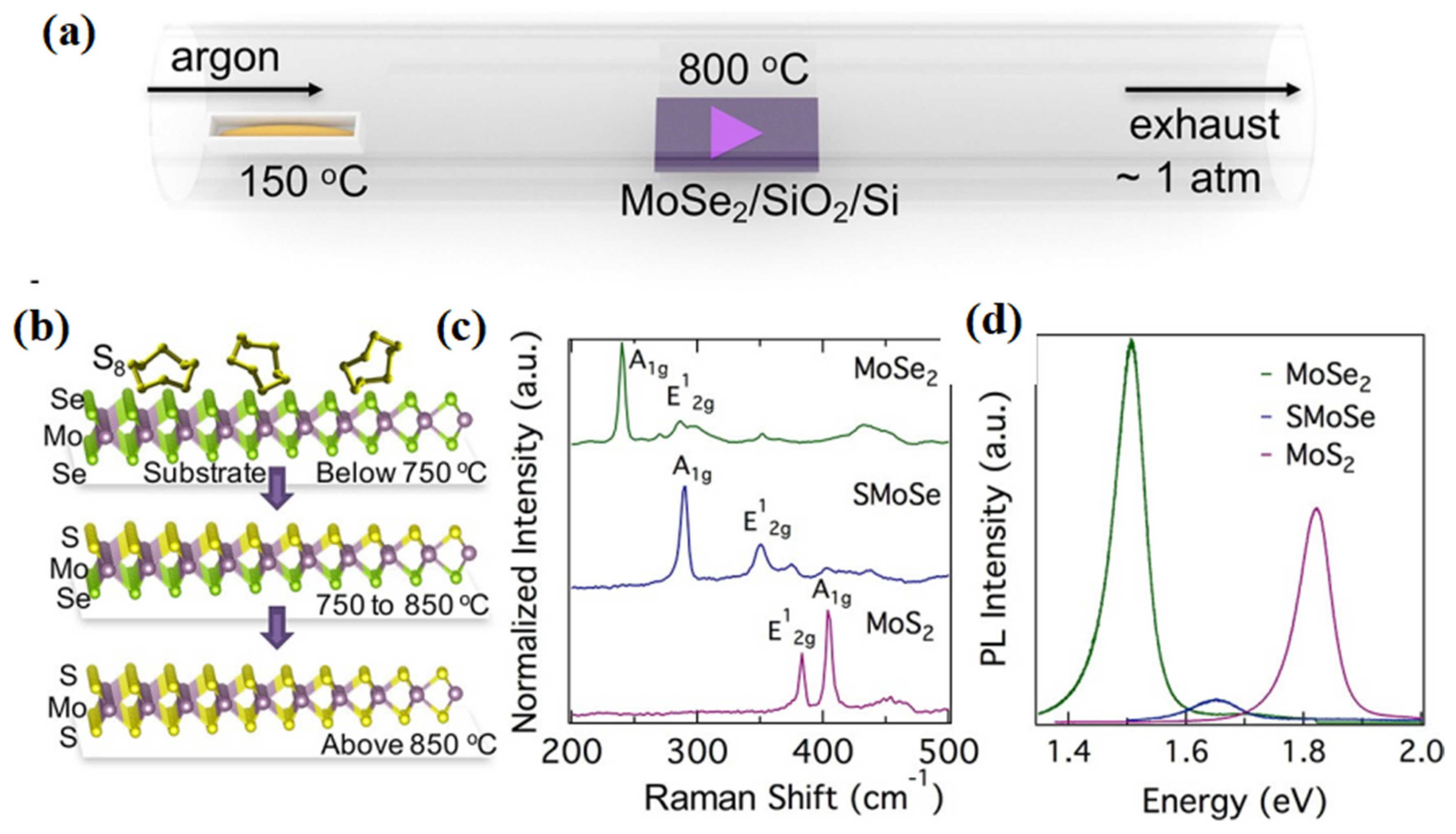
2.1. Chemical Vapor Deposition (CVD)

A range of both bottom-up and top-down approaches have been explored for the synthesis of 2D JTMD monolayers. Top-down methods, such as plasma treatment and selective chemical etching, are adaptations of techniques used for traditional 2D TMDs. However, these processes often face challenges, including defect formation, incomplete reactions, and limited precision in structural control. As a result, there has been a growing shift toward bottom-up strategies, which allow for more accurate manipulation of material properties and structural integrity. Among these, CVD has been shown as a leading technique, recognized for its ability to produce high-quality, large-area Janus monolayers with excellent crystallinity, making it suitable for scalable fabrication.
CVD growth can be broadly classified into one-step and two-step approaches [4,5]. In the two-step approach, a monolayer TMD (such as MoS2) is initially fabricated, after which selective substitution of S atoms on one side with Se or Te is carried out in a subsequent step to form the Janus configuration. In 2017, researchers successfully synthesized 2D JTMD monolayers for the first time using two distinct strategies. One of these involved employing H2S during a controlled sulfurization process to partially replace selenium atoms in MoSe2, leading to the formation of a Janus structure under optimized thermal conditions. In this process, the most critical variable control is the choice of temperature and the control of atmospheric pressure. For example, PtSe2 can be converted into Janus PtSeS at 800 °C. In addition, gold foil can also be used as a substrate [6]. First, a single layer of MoSe2 single crystal is grown and then cooled. After annealing at 700 °C under an S vapor atmosphere, S atoms will replace the Se atoms in the bottom layer. In this process, Au plays a role in dissociating S molecules and chemically adsorbing S atoms, which is an indispensable part of the preparation process. In addition, temperature control during the process is also crucial. If the sulfurization temperature is below 700 °C, it shows that this material conversion is incomplete. If the temperature is greater than 800 °C, the Raman spectrum of this material shows that ML MoS2 has a high degree of defects [7]. Under different conditions, the temperature required to control the reaction is also different. We can control the synthesis of the required materials by adjusting the temperature. A specific example can be seen in Figure 1.
For the second method, hydrogen plasma was applied initially to strip and hydrogenate the upper S atoms of the monolayer XS2 and then perform a Se process at a suitable temperature, that is, using Se atoms to replace the top H atoms [8]. Scientists have used this method to make Janus MoSSe monolayer materials. First, a single-crystal triangular molybdenum disulfide (MoS2) monolayer is fabricated using chemical vapor deposition, and then a remote hydrogen plasma is employed to remove the top S atoms and replace them with H atoms. Thermal selenization occurs under vacuum, where Se atoms replace the hydrogen atoms, leading to the fabrication of a stable Janus MoSSe single atomic layer [9]. The Selenization temperature of this process is critical. The temperature of the substrate must be over 350 °C to form Mo-Se bonds, but if the temperature is too high, above 450 °C, the material structure will be unstable. From this point, it can be analyzed that the process of this method does not focus on thermodynamics, but on the control of kinetics and this ensures controllability during the replacement process. A major benefit of the two-step synthesis approach is that the TMD monolayer is synthesized first, allowing for highly controlled substitution of the upper-layer elements. This ensures that the resulting monolayer JTMDs are highly crystalline. Furthermore, the method can be used to enable a controlled fabrication of multilayer structures. However, the two-step approach comes with certain limitations. The sequential processing steps lead to prolonged synthesis time and increased cost, a more complex fabrication process, and challenges in mass production in industrial settings. Future advancements in this method would focus on optimizing the second-step substitution mechanism to improve efficiency, minimize reaction time, and reduce undesirable side reactions, thereby making the process more feasible for large-scale applications. Researchers have made a series of optimization improvements, such as combining with MBE method and SEAR technology can improve control accuracy. A NaCl-assisted process was employed to achieve the growth of Janus MoSSe monolayers by precisely controlling the in situ temperature. This approach significantly simplifies post-processing procedures and provides a straightforward, economical, and effective approach way for the synthesis of 2D JTMDs [10].
The one-step synthesis method follows a similar principle to the two-step approach, but with a key difference: in this method, the transition metal sources directly react with two distinct chalcogen precursors (e.g., S and Se) instead of sequentially replacing chalcogen elements at high temperatures in a single step, resulting in the formation of the Janus structure. In this process, the form of the Janus structure utilizes the different reactivity of chalcogen precursors at high temperatures. The key advantage of the one-step synthesis method over the two-step approach is its simplicity—the entire process is completed in a single step, enabling it more applied to large-scale industrial production. However, due to the varying chemical activities and diffusion rates of different chalcogen gases at high temperatures, achieving precise atomic substitution on both sides of the monolayer remains a challenge. This can result in non-uniform material distribution and make it difficult to obtain high-quality monolayers. To address these challenges, researchers are focusing on optimizing gas flow dynamics and temperature control to enhance the controllability and uniformity of the one-step synthesis process.
Figure 1. (a) Schematic diagram of the reaction process. (b) Synthesis of MoSSe by chemical vapor deposition. (c) Raman spectra comparison of MoSe2, Janus SMoSe, and MoS2. (d) Photoluminescence (PL) spectra of the three materials under 532 nm diode laser excitation, illustrating differences in their optical properties. (Green, blue, and purple represent MoSe2, SMoSe, and MoS2, respectively)Reprinted with permission from [11]. Copyright 2017 American Chemical Society.
Crystals 15 00567 g001
Overall, CVD offers unparalleled crystallinity and scalability for JTMD synthesis, especially its two-step approach that allows for high structural precision. The maturity of CVD and its compatibility with industrial processes make it the most widely used technique. However, precise control of substitution sites requires tight control of gas flow, temperature, and substrate interactions, which increases the complexity of the process. High-temperature processes may also limit the choice of substrates. Nevertheless, continued innovations such as NaCl-assisted growth and MBE integration are addressing these issues and pushing CVD toward practical industrial applications.

2.2. Pulsed Laser Deposition (PLD)

Although the two previous methods successfully synthesized 2D JTMD materials, they were synthesized in a high-temperature environment, which easily caused certain damage to the material structure and even cracks and had certain limitations on the synthesis in material heterojunctions. PLD is a general method for synthesizing thin films. Generally, a target material containing the desired transition metal and chalcogenide is bombarded with a high-energy pulse laser to form a plasma, and then the plasma cloud is condensed and deposited on the substrate to form a Janus structure film. (As shown in Figure 2) Compared with other manufacturing methods, this method has a lower temperature (only 300 °C). Under the condition of controlling Se and Ke, it can complete the preparation of high-quality Janus TMDs single-layer materials (such as WSSe) by repeatedly injecting and then recrystallizing. This is a low-kinetic energy process, and the complete replacement of atomic layers can be achieved by controlling the kinetic energy [12].
The PLD method is one kind of physical vapor deposition technique that offers exact controllability for the thickness and chemical makeup of the synthesized film by adjusting key parameters such as laser power and deposition rate. This high level of control makes PLD particularly applicable to the layer-by-layer synthesis of multilayer JTMDs and integrates them with other 2D materials, such as graphene, to construct heterojunction structures [13]. Although PLD offers distinct benefits, it faces problems that limit its viability for large-scale industrial use. High costs associated with laser equipment and vacuum systems present significant barriers to economic production. In addition, PLD generally yields slower deposition rates than CVD, which impacts its efficiency for mass fabrication. Its inherent nature as a physical deposition process also complicates the direct synthesis of Janus structures. Consequently, supplementary techniques, such as targeted etching or plasma-based modifications, are frequently necessary to induce the desired asymmetry and fine-tune the structural and functional properties of JTMDs.
To overcome these limitations, extensive research has focused on enhancing both the scalability and precision of the PLD method. Approaches such as plasma-assisted deposition are being explored to enable real-time modulation of Janus structures during film growth. Meanwhile, developments including laser scanning techniques, multi-target arrangements, and other system-level optimizations have been proposed to achieve both uniform and large-area Janus film deposition. Additionally, post-deposition modification strategies are gaining attention, especially for enhancing the structural robustness and long-term stability of Janus materials. Techniques like controlled degradation and plasma modification are employed to fine-tune the physicochemical properties. Collectively, these developments hold promise for advancing PLD as a viable route for the synthesis and integration of two-dimensional JTMDs in next-generation electronic and optoelectronic technologies.
PLD has good thickness and composition control capabilities under low-temperature conditions and is particularly suitable for building heterojunction structures and device integration. Its layer-by-layer deposition characteristics make the structure control more precise. However, the deposition rate of this technology is relatively slow, and the equipment cost is high, which is not conducive to large-scale promotion. At the same time, the additional plasma treatment or post-modification steps required to achieve the Janus structure increase the process complexity. If breakthroughs can be achieved in equipment design and real-time reaction control in the future, it is expected that this method will be expanded from laboratory research to industrial application.
Figure 2. (a) Schematic of the synthesis route for the intermediate MoSH and the Janus MoSSe monolayer, highlighting the hydrogen plasma treatment using inductively coupled plasma (ICP). (b) Diagram of the selenization process, where the sample is transferred between the low-temperature ICP zone and the high-temperature furnace center using a custom-built magnetic manipulator without destroying the vacuum environment. Reprinted with permission from [14]. Copyright 2021 American Chemical Society. (c) Experimental setup for generating and directing Se plasma plume inside a vacuum chamber. A 248 nm excimer laser (25 ns pulse, 1 Hz, 1 J/cm2) strikes a 1-inch Se target at a 30° angle, producing a highly directional plume. An ICCD camera and a movable ion probe are used to monitor the interaction with CVD-grown WS2 monolayers. (d) False-color, time-gated ICCD images of the Se plasma reveal its dynamic propagation in vacuum and under argon background pressures of 10, 20, and 50 mTorr. (Different colored lines represent different pressure backgrounds as shown in the figure) The gate width is set to 10% of each delay time, and intensity is normalized for comparison. (e) Distance-time (R-t) plots derived from ion probe currents illustrate the front-edge motion and deceleration of the plasma plume under varying argon pressures. (f) Schematic of the PLD process used to synthesize Janus MoSSe monolayers. (g) Structural schematic diagram of MoSSe material during PLD process Reprinted with permission from [12]. Copyright 2020 American Chemical Society.
Crystals 15 00567 g002

2.3. Selective Epitaxial Atomic Replacement (SEAR)

The SEAR is an advanced material synthesis technique that integrates selective epitaxial growth with atomic layer replacement to achieve highly controlled fabrication of 2D JTMDs. The process is primarily divided into two key steps. First, a monolayer TMDS is synthesized on the substrate using CVD or molecular beam epitaxy (MBE). Then, a selective atomic layer replacement is performed using chemical vapor or plasma-assisted techniques, leveraging the different chemical reactivities of chalcogen elements to achieve precise atomic substitution. Notably, the entire process can be conducted at relatively low temperatures (~300 °C), thereby minimizing potential material degradation caused by excessive heat. Recently, some scientists used SEAR to prepare Janus TMDS materials at room temperature. This method is also kinetically driven, using inductively coupled plasma (ICP) to generate H radicals to generate selenium vacancies. In this process, the properties of H radicals and ICP are very important [15]. Because under high-temperature conditions, 2D JTMD materials are more easily converted into 2D alloys. This method first grows MSe2 through CVD and then generates Se vacancies through hydrogen radical adsorption and combination generated by inductively coupled ICP. Subsequently, S molecules are introduced and dissociate to form active S radicals, which facilitate the formation of a stable Janus MSSe2 monolayer. Compared to conventional two-step CVD processes, the SEAR approach enables more precise atomic replacement on the monolayer surface, resulting in improved structural uniformity. Additionally, the lower reaction temperatures and gentler processing conditions help suppress the development of interlayer defects, which is an important factor for fabricating high-quality heterojunctions. An added strength of SEAR is its adaptability to both CVD and MBE platforms, enhancing its ability for scalable and uniform synthesis of large-area 2D JTMDs.
SEAR combines the precise growth and selective atomic replacement of MBE or CVD to achieve low-temperature, low-defect Janus material construction, which is particularly suitable for designing heterostructures. This method can effectively control the composition difference between the upper and lower surfaces of the material, but the required equipment (such as an ICP source) is complex and the processing efficiency is limited. Although SEAR has obvious advantages in structural control, if mass production is to be achieved, technical optimization is still needed in terms of process simplification and material yield improvement.

2.4. Room Temperature Atomic Layer Substitution (RT-ALS)

RT-ALS represents a gentle chemical approach based on solution-mediated anion exchange processes. The process begins by selecting an appropriate TMD monolayer as a precursor, followed by precise control of solution concentration, reaction time, and temperature in a medium containing Se2− or Te2− ions, and finally achieves the goal of selective atomic replacement on one side of the monolayer. Alternatively, it can be replaced by low-pressure vaporization. To enhance structural stability, post-treatment steps such as annealing are typically required. Similar to the previous method, this method is also achieved through H radicals. In the first step, the TMD monolayer was synthesized at about 625 °C using the CVD system, but after that, the chalcogenide chemical atoms on the top layer of the material are stripped in a mild chemical manner through hydrogen plasma, and the supply of chalcogenide substitutes is promoted in a low-pressure environment to replace the missing atoms, and finally a Janus TMDS structure material is obtained at room temperature [16]. The advantage of this process is that the reaction can be guided through different pathways. Scientists have successfully converted WS2 into Janus WSSe using this method. It has been verified that this is also a general method that can be applied to synthesize JTMD materials. Moreover, as a result of the active activity of H radicals, the reaction process reduces the reaction barrier, so the energy barrier is much lower. In the process of converting MoS2 to MoSSe, H radicals are first adsorbed on the MoS2 monolayer, and then two H atoms form bonds with S atoms. In the subsequent process of H2S desorption to form S vacancies, the minimum activation energy barrier is less than 0.5 eV, which is much smaller than the 2.5 eV of Mo-S bond breaking in the high-temperature pathway, so the substitution process can be completed at room temperature, which avoids the damage to the original lattice structure in a high-temperature environment and can also be used to synthesize some materials that are difficult to grow directly and synthesize by CVD method at room temperature. In addition, this method can also use a combination of photolithography and flipping to construct a variety of heterojunction structures. One of the key advantages of RT-ALS is its suitability for large-scale synthesis, which makes it suitable for a broad range of TMDs and holds promise for industrial production. RT-ALS was utilized to successfully synthesize Janus MoSSe on various substrates, enabling the exploration of its promising applications in lithography and microelectronic devices. Especially, the successful fabrication on a Ti-Au conductive substrate highlighted the distinct differences in the growth mechanisms of Janus TMDs on insulating versus conductive substrates. This research not only provides new insights into the interaction between plasma and materials but also provides a novel approach for leveraging 2D materials in the fabrication of electrochemical micro-reactors [17]. However, due to diffusion effects during the solution-based reaction, ensuring uniformity in the replacement process remains a challenge. Researchers are actively exploring more efficient ion exchange strategies or integrating RT-ALS with CVD and MBE techniques to enhance reaction controllability, which lays the foundation for scalable and high-quality synthesis.
Overall, RT-ALS relies on mild liquid-phase anion exchange reactions to achieve the synthesis of Janus materials at room temperature, effectively avoiding the problem of lattice damage. Its process cost is low and it is suitable for large-area and large-scale preparation, especially in terms of patterning and compatibility with conductive substrates. However, this method still faces problems such as uneven ion diffusion and difficult control of the reaction interface. The current research direction is to combine RT-ALS with patterning processes or gas-phase-assisted processing to improve its reliability and consistency in large-scale applications.

2.5. Construction Methods of Heterojunction Structures

The heterojunction structures of TMDs have received a lot of attention for their unique electrical, optical, catalytic, and interlayer interaction features [18]. Particularly, the heterojunctions constructed from JTMDs combine the intrinsic advantages of TMDs with the unique properties introduced by structural asymmetry, thereby unlocking enhanced functionalities. As a result, deeper research has been devoted to developing versatile fabrication methods for constructing diverse heterojunction configurations, with promising applications in nanoscience, optoelectronics, and catalysis. One common approach involves direct sulfidation or selenization to obtain either lateral or vertical heterostructures. Alternatively, a two-step transfer technique has been employed: MoS2 is initially synthesized via CVD and subsequently subjected to selenization to form monolayer MoSSe. This Janus layer is then transferred onto a MoS2 substrate, resulting in a heterostructure characterized by dual interfaces, namely S/S and S/Se. [19]. Scientists have used the above-mentioned SEAR method to construct Janus 2D structures and used polymer-assisted methods to further improve the problem of Janus vertical heterostructure limitations [20]. The room temperature conditions of SEAR effectively avoid unexpected situations when synthesizing alloys at high temperatures. In addition, the RT-ALS method described above can be combined with photolithography and flip transfer processes. This method provides a new method for constructing different heterojunction structures at different locations. The development of bandgap engineering and predictive modeling for 2D material heterojunctions is advancing rapidly. In the future, researchers will combine machine learning, artificial intelligence, and the integration of advanced density functional theory (DFT) simulations with experimental validation to close the gap between theoretical predictions and practical applications, and scalable technologies. The ultimate goal is to seamlessly incorporate 2D heterostructures into existing semiconductor technologies, unlocking their full potential in next-generation electronic, optoelectronic, and energy applications [21]. In summary, scientists have also proposed many new methods for the construction of heterojunction structures of 2D JTMDs. These methods provide a good foundation and prerequisite for researchers to further study and explore the unique structural characteristics and practical applications of 2D JTMDs. (The heterojunction band is shown in Figure 3)

3. Atomic Structures of 2D JTMDs

The symmetry of the structure is vital in shaping the electronic band gap, crystal structure, and other physical properties of 2D materials. While monolayer TMDs already exhibit notable in-plane asymmetry, which imparts unique features to their electronic band structures, optical behaviors, and spin-related interactions, the advent of two-dimensional JTMDs further extends this paradigm by incorporating out-of-plane structural asymmetry. This added degree of asymmetry enables a new class of properties that surpass those achievable in traditional 2D materials [23]. As a result, the synthesis of 2D JTMDs has become a promising and effective strategy for breaking mirror symmetry and engineering novel functions.
In order to harness the distinctive characteristics of JTMDs, significant efforts have been directed toward the development of sophisticated synthesis methods and the in-depth investigation of their fundamental physical mechanisms. These efforts have not only deepened our understanding of 2D JTMDs but also paved the way for their integration into advanced technological applications. The following section provides a comprehensive summary of their key characteristics and the progress made in their synthesis and exploration.

3.1. Asymmetric Structure

One of the most important features of 2D JTMDs is their inherent structural asymmetry. These materials consist of a single transition metal lying between two different chalcogen elements, such as S and Se, which leads to the absence of mirror symmetry along the vertical direction and distinguishes them from their conventional TMDs. This lack of symmetry results in chemically distinct top and bottom surfaces, generating an intrinsic dipole moment and vertical polarity. Consequently, a built-in vertical polarization field is established, which serves as a crucial part of tuning the electronic properties of the material.
Compared with their symmetric TMDs, JTMDs typically have reduced band gaps and support more efficient charge excitation and transfer processes, which makes them highly suitable for optoelectronic devices. Moreover, the presence of an intrinsic out-of-plane polarization significantly influences the Fermi level positioning and charge transport behavior, offering greater flexibility in modulating carrier dynamics and optimizing electronic performance. This intrinsic polarization effect can be leveraged to develop self-powered optoelectronic devices. Additionally, the destroying of mirror symmetry in 2D JTMDs makes a coupling between electron spin and momentum, resulting in asymmetric spin polarization. This unique property holds significant potential for spintronic applications, offering new opportunities for next-generation quantum and spintronic devices [24].

3.2. Atomic Structure of JTMDS

People have tried to apply various spectral techniques to study the structure and other properties of materials, among which Raman spectroscopy is a very common technical means. As shown in Figure 1c, after analyzing the Raman spectrum for 2D JTMD materials, people found that due to symmetry breaking, it has mode splitting and Raman peak shift compared with traditional TMD materials [25]. Because of the various chemical compositions of the upper and lower surfaces, the masses and bond lengths of the atoms are different, which leads to the splitting of the atomic vibration mode, showing different characteristics in two directions, resulting in the vibration originally belonging to one mode being split into two or more frequencies. The same reason may also cause the original Raman peak to shift significantly. In addition, the different intensities of the split Raman peaks reflect the activity of different vibration modes, and the movement of the new Raman peak depends on the different masses of the chemical bond. People have performed relevant research on MoSSe materials [26]. In the E2g mode, which corresponds to in-plane vibrations, the asymmetry introduced by the different atomic masses and bonding strengths of S and Se atoms on opposite sides of the Janus monolayer leads to a frequency splitting. This results in two distinct vibrational modes, observable as a splitting of the original single Raman peak. Similarly, in the A1g mode, which involves vertical vibrations, the asymmetry in chemical environments above and below the central metal layer causes nonuniform interlayer forces. While in conventional TMDs the central Mo atom oscillates symmetrically relative to identical S atoms, in JTMDs, the symmetry is destroyed, resulting in the splitting and shifting of A1g Raman peak [9]. The observed Raman mode splittings and frequency shifts reveal differences in bonding interactions and vibrational characteristics within the lattice, offering critical insight into the mechanical robustness of the material. Furthermore, Raman spectroscopy is a precise and non-invasive strategy for detecting alterations in the electronic band structure, making it an essential method for detecting the optoelectronic features of 2D JTMDs.
Furthermore, STEM and AFM are widely employed for analyzing the atomic-scale structure of Janus materials. (As shown in Figure 4) Particularly, high-angle annular dark-field scanning transmission electron microscopy (HAADF-STEM) facilitates direct visualization of atomic arrangements in monolayer JTMDs, allowing for precise structural analysis. In addition, if integrated with electron energy loss spectroscopy (EELS) and energy-dispersive X-ray spectroscopy (EDS), the spatial distribution of chalcogen elements such as S and Se can be distinctly resolved. These compositional mappings verify that S and Se are, respectively, positioned on opposite sides of the transition metal plane, thus affirming the intrinsic structural asymmetry characteristic of Janus materials [9]. Beyond imaging, STEM also allows for quantitative assessment of point defects, atomic vacancies, lattice distortions, and the precise measurement of bond lengths and interlayer separations. For example, in MoSSe monolayers, substitutional differences between S and Se are directly linked to variations in the electronic band structure. Furthermore, STEM proves effective in studying van der Waals heterostructures and elucidating interlayer coupling effects in stacked Janus TMDC systems [27].
In addition, compared with bilayer TMD materials, the interlayer coupling of the low-frequency Raman mode of the Janus heterojunction structure is enhanced, which is confirmed to be caused by the reduction in the interlayer distance, resulting from the intrinsic dipole moment. The enhanced interlayer coupling of the stacked heterojunction has a good promoting effect on the development of optoelectronic devices [28].
In addition, due to the asymmetry of Janus, its substrate presents great sensitivity to the chemical environment. The out-of-plane dipole can react strongly with the adsorbed molecules, thereby enhancing the Raman reflection and causing the activity of the Raman mode to change. In addition, the Raman spectrum of Janus is also sensitive to temperature. These characteristics make Janus materials regarded as another powerful development path for biomolecular sensors.
Researchers often employ a combination of spectroscopic techniques to investigate the structural characteristics of Janus 2D materials. For instance, photoluminescence (PL) spectroscopy has been used to study MoSSe, revealing that the PL peak of monolayer MoSSe appears at approximately 1.68 eV, which lies between the emission peaks of MoS2 and MoSe2. Additionally, the PL intensity of MoSSe is significantly weaker compared to these two materials, indicating a decrease within the energy band gap of MoSSe. Similar trends have also been observed in WSSe, further supporting this conclusion. The suppression of PL intensity is likely attributed to the internal out-of-plane electric field generated by the structural asymmetry of the Janus configuration, which hinders electron-hole recombination, thereby reducing PL emission. This phenomenon suggests an enhancement of exciton effects, which serves a crucial part in the progress of photovoltaic devices and photoelectric detection technologies, as shown in Figure 1d and Figure 3 In addition, AFM, HRTEM, and XPS are also often used to analyze the atomic structure and electronic band gap of 2D JTMDs.
In addition to experimental characterization, understanding the atomic structure of 2D JTMDs requires a group-theoretic perspective, especially their crystallographic symmetries and space group classification. Conventional TMD monolayers, such as MoS2 or WS2, typically exhibit D3h point group symmetry and belong to space group P6m2 (No. 187) due to mirror symmetry about a horizontal plane through the metal layer. However, in Janus structures (such as MoSSe), the mirror symmetry is broken due to the top and bottom chalcogen layers being composed of different elements. As a result, the overall point group is reduced to C3v, and the space group symmetry is typically lowered to P3m1 or other related subgroups, depending on the atomic arrangement and stacking structure [29]. In addition, many Janus structures also exhibit the P3m1 space group, which is beneficial for designing and modulating the excitonic properties of chalcogenides [30,31]. Apart from the P6m2 space group, TMD monolayers can also adopt the P63/mmc space group (2H phase). Correspondingly, Janus TMD (JTMD) monolayers can still exhibit the P63/mmc space group (2H phase). However, compared to TMD monolayers, the broken mirror symmetry in JTMD monolayers endows them with many unique properties. For example, MoSSe undergoes an isostructural phase transition under pressure, and its electronic structure changes much more significantly than that of MoS2 under the same conditions [32,33]. It is worth noting that although most JTMD monolayers exhibit hexagonal structures, there are also some JTMDs, such as Pd and Ni [34] based variant structures, that can exhibit unique pentagonal configurations. This structure is different from the 1H and 2H phases and can exhibit anisotropic light absorption characteristics and good optoelectronic properties. In addition, its monolayers also play a good role in photocatalytic water splitting [35] and electrocatalysis [36]. This symmetry reduction has profound consequences for vibrational, optical, and electronic properties. For example, previously degenerate phonon modes may split due to the loss of inversion or mirror symmetry, as observed in Raman spectroscopy. Furthermore, in layered Janus structures or heterostructures, symmetry considerations are also crucial to determine interlayer coupling and band alignment. Classification into structural families such as 1H (hexagonal, trigonal prismatic coordination) or 1T (octahedral coordination) remains valid, but the asymmetry of Janus materials introduces distinct distortions and local dipole moments that distinguish them from symmetric materials.
In summary, group symmetry analysis not only provides a theoretical framework for predicting physical properties but also supports the interpretation of spectroscopic and microscopic data, thus reinforcing the intrinsic uniqueness of 2D Janus TMD materials.

4. Properties of 2D JTMDs

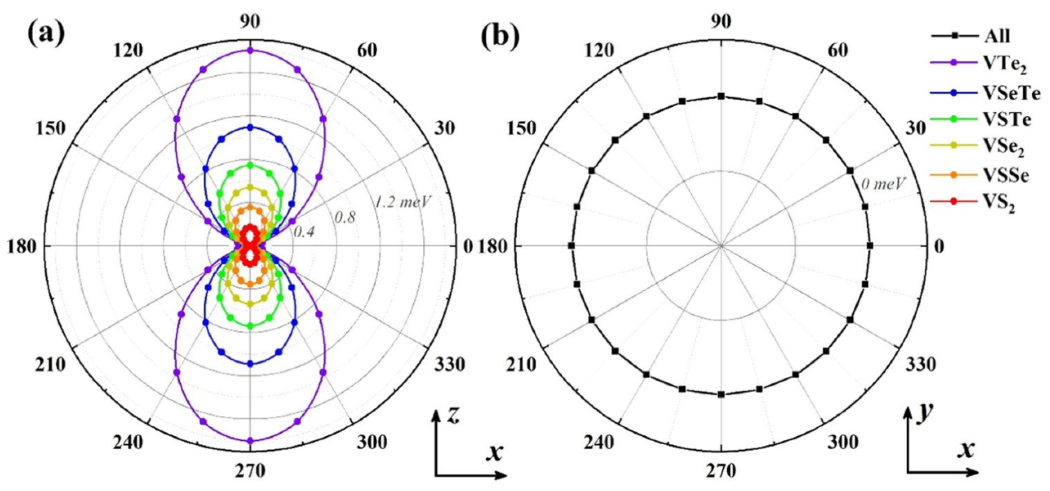
4.1. Interlayer Dipole Moment

The dipole moment is a physical quantity that describes the asymmetric charge distribution in a system. Two-dimensional JTMDs have an asymmetric out-of-plane structure. Owing to the variation in atomic size and electronegativity between the top and bottom chalcogen layers, the Janus monolayer molecular structure has an out-of-plane vertical dipole moment.
The exciton formation rate in MoSSe was found to be about 30% faster than that in MoS2. In the material, excitons are mainly formed by optical phonon scattering. The accelerated exciton form can be concluded that optical phonon scattering is promoted by the built-in dipole moment of the Janus material. By studying MoSSe and WSSe in 2D JTMDs, and after studying the exciton dynamics and optical characteristics of the corresponding single-layer structures, scientists found that due to its intrinsic dipole moment, the electron and hole wave functions in the material are forced to separate, which reduces the spatial overlap, so the strength of the exciton oscillator is also reduced. Moreover, the existence of a pronounced built-in dipole moment significantly enhances light–matter interactions, thereby prolonging the radiative recombination lifetime of excitons. This extended lifetime is advantageous for boosting the efficiency of optoelectronic devices including photovoltaic cells and light detectors. Additionally, the built-in dipole facilitates effective spatial separation of charge carriers, providing valuable potential for the design of advanced charge-collecting electronic systems [37]. In addition, the out-of-plane dipole moment induces band bending and shifts in the Fermi level. By leveraging the Stark effect, researchers can modulate this dipole through the external electric field, thereby tuning the optical transition energies and tailoring the optical response of Janus structures. The dipole characteristics in 2D JTMDs can be directly examined using DFT simulations or experimentally probed via Kelvin probe force microscopy (KPFM) [38]. A novel parameter, formulated based on intrinsic atomic characteristics such as atomic number and radius, has recently been proposed to approximate dipole moments in both monolayer and multilayer Janus structures. This approach reveals the link between atomic configurations and dipole strength, allowing for rapid screening and evaluation of band alignments in 2D JTMD materials. It offers a theoretical foundation for the rational design of emerging 2D electronic systems and will serve as a practical strategy for adjusting the electronic behavior of the Janus structure [39].

4.2. Rashba Effect

The Rashba effect originates from spin–orbit coupling (SOC) and is a prominent characteristic in Janus 2D TMDs. Its significant manifestation stems from two main factors: the asymmetric distribution of chalcogen elements distributed between the upper and lower atomic planes disrupts spatial inversion symmetry, thereby amplifying Rashba spin splitting; additionally, this lack of symmetry induces a vertical electric field and a resultant dipole moment, which further strengthens the effect. This internal electric field greatly enhances the spin–orbit coupling effect of electron orbit. Furthermore, the TMDS material itself also exhibits pronounced spin–orbit coupling, while the strong quantum confinement inherent to the 2D structure further enhances the Rashba effect.
Since 2D JTMD materials were first manufactured, scientists have believed that they hold significant promise in the applications of spin electronics. They have applied first principles to systematically study their SOC effect, local potential gradient, Rashba effect, and system stability, using phonons and molecular dynamics [40].

4.3. Vertical Piezoelectricity

Piezoelectricity is a unique property that enables the conversion between mechanical and electrical energy. The piezoelectric phenomenon is categorized into the positive piezoelectric effect and the converse piezoelectric effect, which can be caused by the positive charge generated by the mechanical stress on the material and the deformation caused by the electric field on the material. It is an intrinsic coupling effect between strain and electromechanical responses that exists in semiconductors and insulators [41]. This phenomenon arises due to the absence of inversion symmetry in the crystal structure, which enables the generation of electric polarization under mechanical deformation. Materials with this property have been widely used in electronic techniques including sensors and energy fields. In traditional TMDs, the piezoelectric effect of in-plane piezoelectric technology is realized, and there are many materials with strong piezoelectric coefficients. They have great potential in the corresponding electronic device field [42]. The piezoelectric properties of TMDs have been effectively utilized in flexible nanogenerators, enabling the transformation of small-scale mechanical energy into electrical output for self-powered electronic devices [43]. Moreover, their excellent piezoelectric performance has demonstrated promising applications in optoelectronic devices [44], piezoelectric memory, transistors, biosensors, and human–computer interaction electronics [45]. Looking ahead, advancements in multifunctional composite materials and integrated manufacturing technologies will further drive the development and optimization of piezoelectric TMD-based devices. However, the piezoelectric polarization effect of traditional materials is limited to the basal plane, which cannot perform vertical piezoelectric operation.
However, since the atoms on either side of a Janus monolayer have different electronegativity and atomic radius, the overall spontaneous electric dipole moment appears, thus breaking the mirror symmetry. The single-layer or multi-layer structure of 2D JTMDs can achieve out-of-plane piezoelectric effect. Because of the spontaneous polarization effect, the piezoelectric properties of Janus materials are greatly enhanced, and the piezoelectric coefficient is higher. Under the action of stress, the material will generate a stronger potential difference in the vertical direction. Usually, the piezoelectric coefficients of single and multilayer Janus chalcogenides under uniaxial or multiaxial strain can be calculated by first principles. Traditional MoS2 materials can only be polarized in the plane, and their piezoelectric coefficients e11 and d11 are 3.56 and 3.34, respectively. Janus MoSSe, on the other hand, has e11 and d11 of approximately 3.74 and 3.76, respectively, and also has piezoelectric coefficients e31 and d31 of approximately 0.032 and 0.020, respectively, showing its out-of-plane piezoelectric properties. It has been verified by research that for a certain MXY multilayer structure, the change caused by e33 (d33) is one order of magnitude higher than that of e31 (d31), which indicates that the vertical piezoelectric polarization caused by vertical strain is much stronger than the in-plane strain [46]
In the case of uniaxial strain, the Janus MXY (M = W, Mo; X, Y = S, Se, Te) single layer has both in-plane and out-of-plane piezoelectricity, and its piezoelectric coefficient is between that of MX2 and MY2 single layers. (As shown in Figure 5)A larger atomic radius of the chalcogen element combined with a smaller radius of the transition metal tends to result in a higher piezoelectric coefficient. Moreover, a greater disparity in atomic size between the two chalcogen atoms further enhances the piezoelectric response. Therefore, after measurement and calculation, the Janus MXY layer of MoSTe and WSTe has the highest in-plane piezoelectric coefficient [47]. Furthermore, first-principles calculations have been employed to investigate the electronic and piezoelectric characteristics of Janus WXSiN (X = S, Se, Te). This study confirmed that variations in the electronegativity of chalcogen atoms result in diversity in Bader effective charges, which consequently influence the piezoelectric coefficients. The calculations further revealed that a higher electronegativity ratio correlates with enhanced piezoelectric performance. Through the study of the built-in electric field, it was also found that the enhancement of the intrinsic electric field leads to an increase in the out-of-plane piezoelectric coefficient. These conclusions provide potential theoretical support for the application of Janus materials in nanoscale piezoelectric devices [48].
For the piezoelectric coefficient of multilayer films, it is the same as that of single-layer films. The larger the radius difference between the X and Y atoms, the higher the piezoelectric coefficient. In addition, an important characteristic of the piezoelectric performance of Janus MXY multilayer films is the interlayer interaction, that is, the polarization effects between different layers influence each other, which is specifically reflected in the superposition or cancelation of van der Waals interaction and electric dipole moment, which will cause the interlayer piezoelectric effect to be divided. For 2H stacking, the in-plane polarization between adjacent layers is opposite, resulting in no in-plane piezoelectric phenomenon in the multilayer film. In addition, as the layer thickness increases, the body effect gradually becomes dominant and the surface polarization effect is weakened. Therefore, the piezoelectric coefficient of the multilayer Janus film is often smaller than that of the single-layer film. Therefore, people often use various methods to regulate the piezoelectric effect of multilayer films, such as adding a vertical electric field between specific layers, changing the direction of interlayer polarization, or changing the piezoelectric coefficient of the multilayer film by changing the material composition through chemical modification.

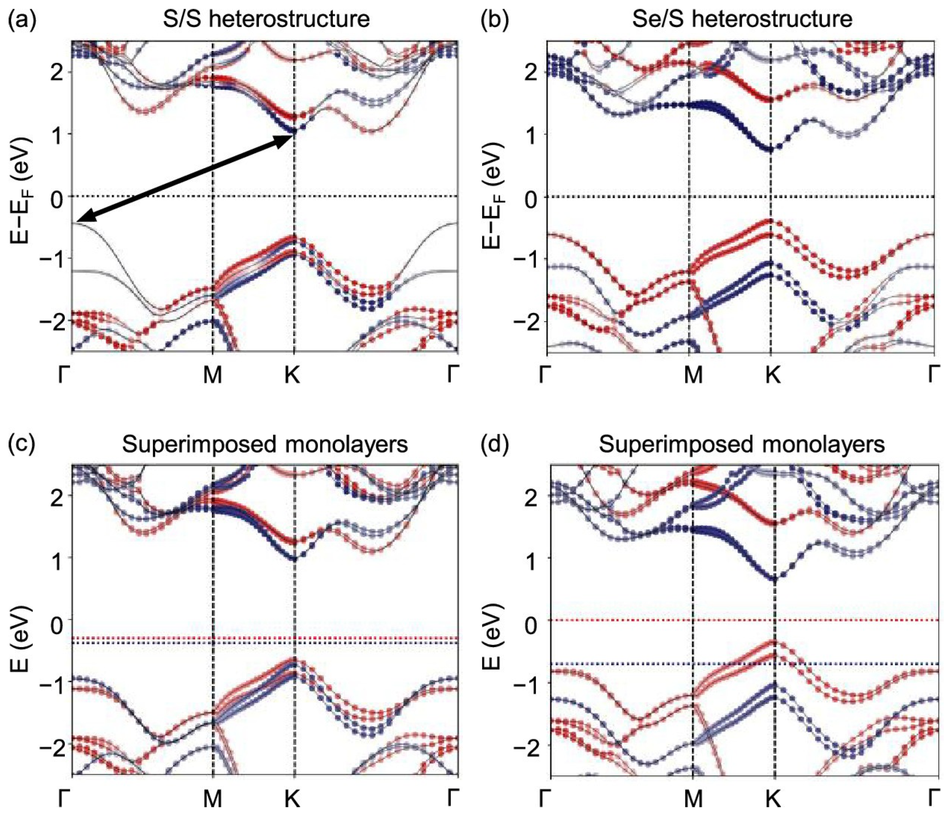
4.4. Two-Dimensional JTMDs Van Der Waals (vdW) Heterojunction Structure

Vdw heterojunctions refer to heterostructures created by stacking different 2D layered materials through van der Waals interactions. This assembly method overcomes the lattice-matching constraints inherent in traditional epitaxial growth techniques, enabling the integration of diverse materials with distinct properties. Moreover, such heterostructures offer optimized band alignment and efficient charge transfer, making them highly valuable for advanced optoelectronics and nanoelectronics [49,50]. The Janus TMD-based van der Waals heterojunction (JTMDs vdW heterojunction) leverages the unique characteristics of JTMD materials in combination with heterojunction engineering. The intrinsic out-of-plane polarization field in JTMDs enhances interlayer coupling, while the heterojunction structure provides additional band modulation capabilities. (As shown in Figure 6 and Figure 7) This synergistic effect facilitates more efficient charge carrier separation and tailored band alignment, making JTMD vdW heterojunctions highly promising for applications in optoelectronics, catalysis, spintronics, and phototransistors [51]. Not only that, the optoelectronic and thermal properties of the heterojunction can also be regulated through stacking, straining [52], doping [53], adsorption, etc., so that it can better exert its own characteristics across various applications [54].
To deeply apply its properties, researchers also systematically investigated the impacts of strain modulation in the potential distribution, optical absorption, and electronic band structure of Janus TMD-based heterostructures. The study systematically investigated the effects under vertical compression and biaxial tension across six distinct stacking configurations, offering an important understanding of the function of strain engineering in Janus TMD systems. The application of mechanical strain led to noticeable shifts toward longer (redshift) and shorter (blueshift) wavelengths in the optical absorption spectra, substantially enhancing the peak absorption within the visible spectrum. Notably, compared with unstrained structures, strained configurations exhibit superior solar energy conversion performance. These results highlight the potential of strain-tuned Janus structures in high-performance optoelectronic devices, paving the way for their use in next-generation solar cells and photodetectors [55]. In recent studies, significant attention has been directed toward exploring the excitonic behavior in two-dimensional Janus bilayer systems. Through the application of ultra-high vacuum annealing techniques, researchers have successfully adjusted the van der Waals spacing and modulated the interlayer polarization dynamics. These modifications have led to enhanced coupling between phonons and excitons, as well as stronger interlayer excitonic interactions [56,57,58]. The study revealed the essential influence of the electric field and polarization effects induced by the Janus structure on exciton behavior within heterobilayers. It emphasizes the promising potential of polarization engineering as a strategy for controlling exciton dynamics, offering a pathway toward the development of advanced excitonic devices for applications in optoelectronics and quantum technologies [59].

4.5. Thermoelectric Performance

Thermoelectric performance refers to the capacity of materials for thermoelectric energy conversion, typically quantified by the thermoelectric figure of merit (ZT). Achieving high thermoelectric efficiency requires a combination of elevated electrical conductivity (σ), larger Seebeck coefficient (S), and reduced thermal conductivity (κ). Two-dimensional JTMDs exhibit remarkable thermoelectric properties due to their inherent structural asymmetry, interlayer polarization, and charge transfer effects [60]. The broken structural symmetry in 2D JTMDs induces an enhanced polarization field, which not only increases S but also generates an internal electric field, thereby improving thermoelectric conversion efficiency. Researchers have conducted a detailed comparative analysis of its single-layer phonon thermal transport characteristics [61], including phonon heat capacity, lifetime, and group velocity. Moreover, the different atomic mass between the upper and lower chalcogen layers breaks the symmetry of phonon transport, thereby enhancing phonon scattering and significantly suppressing lattice thermal conductivity. In addition, interlayer polarization limits the available channels for heat transfer, further decreasing thermal conductivity and reducing energy dissipation. The structural characteristics of 2D JTMDs also facilitate improved carrier transport, while their electronic behavior can be effectively modulated through external influences including electric fields, strain engineering [62], and chemical doping. By adjusting these parameters, phonon scattering mechanisms can be optimized, making 2D JTMDs highly suitable for advanced thermoelectric applications. Through the modulation of these external parameters, phonon scattering pathways can be effectively controlled, enhancing the thermoelectric efficiency of 2D JTMD systems. Recently, studies on Janus-based 2D TMD heterojunctions and multilayer structures have revealed that constructing lateral heterostructures can significantly suppress thermal transport, thereby contributing to improved thermoelectric performance [63]. Additionally, strain engineering has been shown to further enhance the ZT value of Janus heterostructures [54]. Moreover, a study examining the impacts of geometric factors on thermal conductivity found that Janus t-PdTe2 shows a significant dependence on both layer thickness and length. As the number of layers increases, the total thermal conductivity decreases, mainly due to the damping of out-of-plane phonon modes caused by interlayer vdW interactions [64]. In summary, 2D JTMDs constitute an emerging material platform with considerable promise for thermoelectric energy harvesting and low-power electronic applications, presenting valuable opportunities for the development of high-performance thermoelectric technologies.

4.6. Nonlinear Optical and Second Harmonic Generation Responses

Nonlinear optical (NLO) phenomena are central to modern optoelectronic technologies, enabling applications from THz sensing to infrared energy conversion. The strength of a material’s NLO response is intimately linked not only to its crystallographic symmetry but also to topological properties such as Berry curvature and band inversion [65]. JTMDs, particularly those in the distorted octahedral 1T′ phase, have recently emerged as compelling platforms for realizing strong room-temperature nonlinearities due to their broken out-of-plane inversion symmetry and nontrivial topological band structures.
In recent experiments, monolayer Janus MoSSe in the 1T′ phase was synthesized through an RT-ALS method, achieving robust structural conversion under ambient conditions. Despite being only a single atomic layer thick (~10–20 µm in lateral dimensions), these films demonstrated remarkably efficient nonlinear behavior across multiple spectral regimes. Measurements conducted using high harmonic generation (HHG), terahertz emission spectroscopy (TES), and second harmonic generation (SHG) consistently revealed dramatic enhancements in nonlinear output when compared to conventional 2H-phase MoS2 or MoSSe. For instance, SHG intensities in 1T′ MoSSe exceeded those in 2H MoS2 by more than twentyfold, while high-order harmonic generation (up to the 18th order) showed enhancements of over fifty times [66].
These enhanced responses are attributed to several interconnected mechanisms. First, the Janus structure introduces a strong built-in electric dipole due to the asymmetry between the top and bottom chalcogen layers (e.g., S and Se), which breaks inversion symmetry and enables even-order nonlinear processes. Second, the topologically inverted band structure in 1T′ MoSSe results in small bandgaps and large Berry connections, significantly boosting interband transition probabilities and enabling efficient nonlinear wave mixing at THz and infrared frequencies. Third, the strong spin–orbit coupling inherent to the distorted 1T′ lattice further enhances optical transitions by lifting degeneracies and promoting spin-selective processes.
In contrast, 2H-phase TMDs, which are topologically trivial and retain inversion symmetry, display substantially weaker second-order responses due to forbidden electric-dipole transitions in the bulk. This comparative analysis underscores the unique advantage of topological and Janus-engineered 2D materials in nonlinear optics.
The successful implementation of RT-ALS synthesis and the direct observation of high-efficiency nonlinear processes in Janus 1T′ TMDs outline a practical route toward scalable, atomically thin nonlinear media. Researchers have shown that cation Janus also has a huge advantage in non-planar second harmonic response [67]. The cation MM’X2 Janus structure has a stronger dipole effect than the anion M2XX’, and its SHG response is also higher than that of the anion. Among all Janus structures in the experiment, GaInTe2 has the strongest SHG response, with d31 as high as 10 490.41 pm V−1. These findings provide a foundational understanding for future designs of NLO materials and suggest promising directions for ultrathin photonic devices, room-temperature THz detectors, and novel photovoltaic technologies based on the bulk photovoltaic effect.

4.7. Charge Density Wave (CDW) Behavior

CDWs are known to occur in certain 2D materials with layered structures, especially those with a 1T-type lattice. Among TMD materials, researchers have explored the CDW of TMD metals under different modifications and conditions and explained their effects on physical properties [68]. In 2H-MoSeH, harmonic phonon calculations at 0 K reveal phonon softening near the Γ point, indicative of a Kohn anomaly, which is a hallmark of CDW behavior. Similar anomalies have been identified in other TMD-based systems such as 1T-MoSH and 1T-WXH, supporting the classification of 2H-MoSeH as a CDW material. Among the proposed mechanisms, Fermi surface (FS) nesting has been widely discussed. However, Lindhard susceptibility analysis in 2H-MoSeH shows that although the real part exhibits a broad enhancement near the Γ point, the imaginary part peaks elsewhere, suggesting that FS nesting alone cannot account for the CDW origin. In contrast, the phonon linewidth γ, which quantifies electron–phonon coupling (EPC) strength, shows significant peaks that coincide with the softened phonon modes, pointing to strong EPC as the primary driver of CDW formation in this material [69]. In addition, researchers also replaced H atoms with Li and systematically studied the stability and electron-phonon interaction properties of MoSLi, including elastic constants and phonon dispersion, further revealing the role of low-energy phonon modes in EPC [70].
Extending this understanding to structurally asymmetric Janus TMDs such as 1T′-MoSSe, the scenario becomes even more compelling. The broken out-of-plane symmetry due to chalcogen atom substitution introduces intrinsic dipole moments and modifies the vibrational and electronic landscape. Theoretical studies suggest that these changes enhance EPC and phonon softening effects, potentially stabilizing CDW phases more effectively than in symmetric counterparts. Additionally, the topologically nontrivial band structure of 1T′-MoSSe provides further electronic instability channels, which may couple with EPC to reinforce CDW formation. Thus, Janus TMDs emerge as a promising class of 2D materials where inversion symmetry breaking, strong EPC, and topological characteristics synergistically facilitate unconventional CDW states, offering rich opportunities for quantum phase engineering and next-generation electronic applications [71].

4.8. Superconductivity

The superconductivity in JTMDs emerges from the intricate interplay of crystal structure, EPC, and competing quantum orders such as CDW. Recent theoretical and computational investigations highlight that the low-dimensional nature and broken mirror symmetry of JTMDs not only support robust EPC but also enhance the tunability of their quantum states via external modulation such as strain or doping.
A key finding is that the superconducting behavior is strongly influenced by the in-plane vibrations of transition metal atoms (e.g., Mo, W), which couple with the electronic states near the Fermi level, particularly those derived from the dz2 and dxy/dx2−y2 orbitals. This coupling leads to soft phonon modes, especially near high-symmetry points in the Brillouin zone, and is responsible for the emergence of superconductivity when CDW order is suppressed. Suppression of CDW through modest strain or carrier doping not only revives metallicity but also induces significant EPC, driving the system into a superconducting phase [69,71].
Additionally, structural variations between the 1T and 2H polymorphs significantly impact the superconducting characteristics. The 1T phase often exhibits stronger EPC and higher critical temperatures due to its flatter electronic bands and more localized vibrational modes, while the 2H phase may demonstrate greater band dispersions and structural stability. The presence of topological edge states and nontrivial Z2 indices in some doped JTMDs suggests a promising avenue toward realizing topological superconductivity [70].
In the future, JTMDs serve as a fertile ground for exploring the competition and coexistence of multiple quantum phases. Their responsiveness to external perturbations allows for fine control over superconducting properties, potentially leading to novel device applications. Further investigations into multigap superconductivity, anisotropic pairing, and the role of spin–orbit coupling could uncover deeper insights into unconventional superconductivity in these materials.

5. Applications of 2D JTMDs

5.1. Sensors

Due to the surface polarization effect and the large surface-to-volume ratio of 2D JTMD materials, they have been regarded as an ideal material choice for gas sensors [72]. Compared with traditional 2D TMD materials, the unique structural characteristics of Janus materials enable the intrinsic dipole to strengthen or weaken the gas adsorption capacity according to the polarization direction. Based on first-principles calculations [73], Researchers have demonstrated that, through theoretical estimation of Janus MoSSe, the uniaxial tensile strain of the material will change the adsorption strength of the gas on the Se layer (S layer). They further found that gas molecules can be adsorbed or desorbed by adjusting the applied tensile strain, primarily due to the variation in electrostatic potential difference induced by the strain. In addition, by using different transition metal atoms, element doping, and vacancy defects [74,75], the electronic structure and dipole moment of JTMDs can also be adjusted to regulate the adsorption performance of the material. All these render 2D JTMD materials extremely high gas sensitivity and strain selectivity, providing a new solution for the research of new high-sensitivity gas sensing nanodevices; in addition, the Janus structure has a strong charge transfer ability, which allows it to work at room temperature and reduce energy consumption. Specifically, it can be used for air quality detection (CO, NO2, etc.) and industrial safety detection (H2, CH4). Recently, researchers have systematically investigated the adsorption behavior of toxic nitrogen-containing gases (NO, NO2, NH3) on intrinsic Janus ZrSSe monolayers as well as those functionalized with transition metals (Au, Ag, Pt). The adsorption mechanisms were explored from multiple perspectives, including charge transfer, adsorption structures, and recovery time, providing a comprehensive understanding of gas–molecule interactions with Janus materials. The study confirmed that metal functionalization primarily significantly enhances gas adsorption, as a result of the strong interactions between metal atoms and gas molecules. Furthermore, first-principles calculations demonstrated that Pt-ZrSSe exhibits excellent sensitivity to NO2, positioning it as an exceptional material for NO2 gas sensing. Additionally, TM-ZrSSe was identified as an effective NO gas sensor, highlighting the potential of Janus-based materials in advanced gas sensing applications. These findings offer valuable theoretical insights for the development of next-generation highly sensitive and selective gas sensors [76].
In addition, the good flexibility and adjustable electronic structure of 2D JTMD materials, when subjected to mechanical strain, variations in the electrical characteristics of the materials can serve as a basis for pressure sensors, especially its unique asymmetric structure, which makes the piezoelectric response of the material stronger and can be used for high-precision pressure sensors. Its flexible and bendable characteristics contribute to potential applications in areas like wearable electronics, robot electronic skin, and flexible sensors in smart bracelets. The pronounced polarization effect of 2D JTMDs makes them highly responsive to the adsorption of biological molecules. The out-of-plane vertical dipole can alter the charge distribution in the adsorbed biological molecules and polarize their intrinsic dipoles, thereby increasing the intensity of Raman vibrations [77]. This clears the obstacles and provides new ideas for the utilization of 2D materials in SERS sensing technology.

5.2. Electronic Devices

Janus materials have been identified as potential candidates for future electronic technologies, primarily owing to their structural asymmetry, intrinsic polarization fields, tunable band gaps, and excellent carrier transport properties. In modern electronic components including field-effect transistors (FETs), one persistent challenge is optimizing the channel material to achieve both high carrier mobility and an appropriate band gap. While conventional monolayer TMDs offer a balance between these properties, enabling their widespread use in FET design, Janus counterparts offer additional degrees of freedom for performance enhancement. However, their intrinsically symmetric structure poses challenges in band gap modulation. In contrast, 2D JTMD materials inherit the advantages of TMDs while introducing unique functionalities. The built-in polarization electric field in Janus structures allows for carrier distribution tuning, thereby enhancing field-effect mobility. Furthermore, the inherent asymmetry of their structure allows for precise tuning of the band gap through external electric fields, mechanical strain, or doping, offering greater control over their electronic and optoelectronic properties. Researchers also found that applying electric field or strain to MoSSe/WX (X = S, Se) heterojunctions resulted in band gap variation and a shift from an indirect to a direct band structure, further confirming the potential of Janus materials in nanoelectronic devices [78]. Atomic layer deposition (ALD) has been utilized to deposit an HfO2 gate dielectric layer on MoTe2, and through an integrated logic circuit model, they demonstrated the diverse functionalities of MoSSe transistors. Their findings highlight the potential for achieving high-performance and low-power Janus-based electronic devices, paving the way for next-generation low-power electronics [79]. Researchers have also conducted in-depth explorations on using insulating materials to prevent Janus stratification in FETs, thereby effectively managing the non-zero net dipole moment of JTMDs and ensuring stability in electronic devices [80].
Beyond electronics, Janus materials also have great promise in optoelectronic devices [81]. The intrinsic polarization electric field in Janus structures promotes efficiently isolating photogenerated electron–hole pairs, thus extending exciton lifetimes and enhancing both photocurrent generation and detection sensitivity—key factors for high-performance photodetectors [82,83]. In addition, the broad tunability of their bandgap allows for wide-spectrum light absorption, making Janus materials strong candidates for next-generation photovoltaic applications [84]. Besides that, first-principles simulations have been used to confirm the excellent electron mobility and optoelectronic characteristics of monolayer JTMDs [85]. For instance, DFT studies show that GaXY (where X, Y = S, Se, Te)/GeAs heterostructures demonstrate significant light absorption spanning the visible to ultraviolet spectrum. Moreover, manipulating interlayer stacking configurations has been shown to influence band alignment and carrier dynamics, offering an additional degree of control in designing efficient solar energy conversion systems [86]. In addition to their roles in transistors and photodetectors, Janus materials hold considerable promise for integration into diodes, memory devices, and energy storage technologies. Their unique structural asymmetry and tunable electronic features enable them versatile platforms for diverse technological domains, reinforcing their potential as key components in future electronic and optoelectronic systems [82,87]. Recently, scientists have also conducted research on the in-plane thermal relaxation characteristics of 2D JTMD materials and their heterojunction structures. It is proved that there is low lattice thermal conductivity in its heterogeneous structure, which can be used in heat transfer [54], and attempts are made to expand the application of JTMDs in thermoelectric devices through various structural engineering [63].

5.3. Spintronics and Valley Electronics
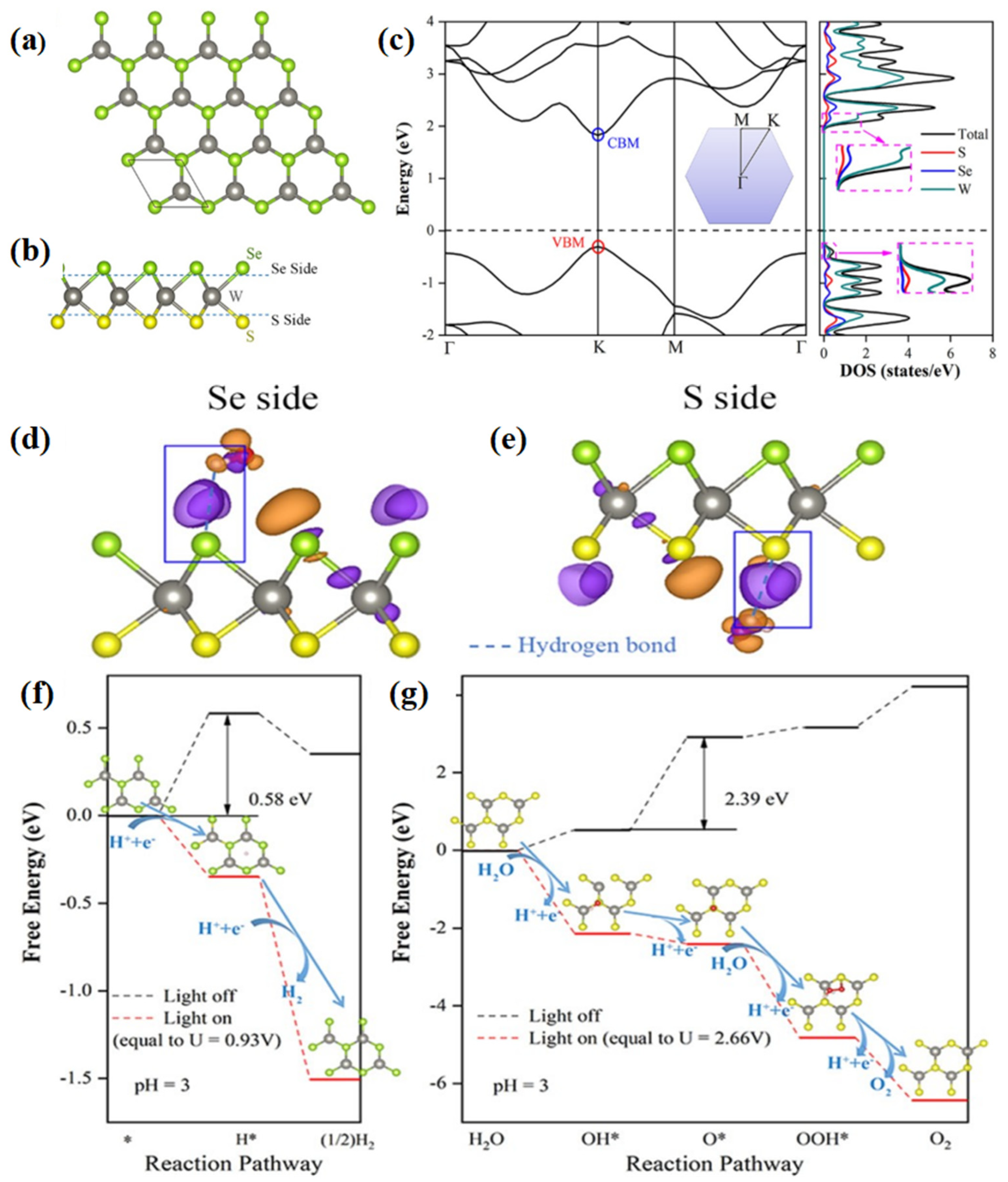
Spintronics is an emerging technology that uses the spin freedom of electrons for information processing and storage. Compared with traditional electronics, 2D JTMD-based spintronics exhibit higher computing speed and smaller device size. As a result of the asymmetric structure of 2D TMDs, the spin–orbit coupling of electrons is enhanced. This induces strong Rashba spin splitting and achieves efficient control of spins. This is of vital importance for the research and development of spintronic devices. Through theoretical research and practical operations, scientists have found that Rashba spin splitting can be efficiently tuned with strain engineering [88], external electric fields, etc [89]. In terms of its application, specifically, its strong spin Hall effect (SHE) can control the spin flow without loss, and control the spin polarization through an external battery, so as to be applied to the design of new spin field effect transistors [90]. This significantly contributes to the advancement of next-generation integrated nanotechnologies and expands potential applications in other spin–orbit coupling-based devices. Using first-principles calculations, researchers have predicted that Janus TMD monolayers CrXTe (X = S, Se) exhibit excellent spin–orbit torque (SOT) functionality and can achieve field-free switching of perpendicular magnetic states. This unique property positions CrXTe as a strong contender for future spintronic technologies, particularly in the progress of spin–orbit torque magnetic random-access memory (SOT-MRAM) and other advanced memory technologies [91]. Through magnetic doping or interface engineering, 2D JTMD materials can also exhibit ferromagnetism, The thermodynamic, kinetic, and mechanical structural stability of two Janus 2D monolayers V3Se3X2 (X = S, Te) as ferromagnetic semiconductors were predicted through first-principles calculations, revealing that these materials exhibit strong ferromagnetism and a high Curie temperature (406 K and 301 K, respectively, both higher than room temperature) [92].
Researchers have also systematically examined the impacts of transition metal atomic defect doping on the structural and magnetic characteristics of Janus WSSe. Their analysis reveals that the ionic radius and electronegativity of the dopant atoms significantly influence the d–p–d orbital hybridization and overall thermodynamic stability in the system. In the context of atomic adsorption, variations in the size of the adsorbed species affect both the adsorption height and the energy levels of defect states, thereby altering stability in the resulting configurations. These theoretical insights provide a foundation for advancing 2D JTMD-based spintronic applications and guiding the design of Janus-derived diluted magnetic semiconductors [93]. Recent studies have identified 2D vanadium-based van der Waals transition metal dichalcogenides (V-TMDs) are promising candidates for applications in spintronics and valleytronics. Investigations into the electronic structure, magnetic behavior, valley polarization, and piezoelectric response of H-phase VXY monolayers (X, Y = S, Se, Te) have revealed that these materials exhibit strong in-plane magnetic anisotropy and are capable of sustaining elevated magnetic phase transition temperatures, highlighting their suitability for spintronic device integration. (As shown in Figure 8) Moreover, the chalcogen elements display right-handed Dzyaloshinskii–Moriya interaction (DMI); however, opposing contributions from chalcogen layers on either side of the transition metal can partially offset one another, resulting in variations in the in-plane DMI component. This complex interplay contributes to a deeper understanding of magnetic anisotropy, spin–valley coupling, and the emergence of near-room-temperature DMI behavior in vanadium-based Janus TMD systems. These findings highlight the potential of H-VXY monolayers for future developments in low-power spintronic and valleytronic devices [94]. Moreover, as spin injection and detection materials, they are suitable for magnetic storage devices such as magnetic tunnel junctions (MJTs), to improve storage density, or use magnetic materials to build spin filters.
Valleytronics represent a class of electronics that uses the valley degree of freedom (band minimum) of electrons for information processing and storage. The focus is on using the valley polarization effect to switch between two valleys to develop electronic devices. The strong SOC effect and asymmetric structure of 2D JTMD materials enhance the valley polarization effect, showing energy extremes at the K and K’ valleys. The valley Hall effect refers to the different directions of electron movement between the two valleys, which generates a net valley current for information storage. In addition, through theoretical research and practical operations, scientists have discovered methods to induce and regulate the valley polarization effect, including the effect of magnetic material substrates, strain effects, and magnetic doping. It is notable that experimental studies have shown that the valley polarization effect can be modulated by altering the stacking order of the Janus layer [95]. Due to these characteristics of 2D JTMD materials, it can excite electrons in the K and K’ valleys through polarized light, thereby constructing valley field-effect transistors with low power consumption and fast logic calculation, realizing information processing and storage; its valley degree of freedom can serve to construct quantum bits and realize ultra-low energy information storage. Two-dimensional JTMD materials have both spin polarization and valley polarization effects, so they have great development potential in spin–valley coupling, such as developing spin–valley logic devices, using spin and valley polarization to store information at the same time, greatly improving information processing capabilities, or using spin and valley degrees of freedom to achieve topological quantum computing, and so on.

5.4. Catalysts

To improve the rate of photocatalytic water splitting, the catalyst is supposed to possess characteristics such as wide-spectrum solar response and high effective electron-hole separation efficiency. In order to find an efficient catalyst, scientists have repeatedly practiced light adsorption, electron-hole separation and charge transfer, and band alignment, and then they confirmed that 2D JTMD materials and their heterojunction structures are ideal catalysts for photocatalytic water splitting [35,96]. Experimental and theoretical investigations have confirmed that Janus WSSe has good performance in catalytic water splitting by calculating the DFT system [97]. Its single-layer band gap just meets the requirements of photocatalytic water splitting, and its absorption rate of visible light is high; in addition, its band edge positions are primarily situated at the Se and S atom sites, and their spatial separation helps prevent the recombination of photoexcited charge carriers. (As shown in Figure 9)Compared with traditional similar TMDs, WSSe has a smaller exciton binding energy and higher carrier mobility, which is more conducive to carrier separation and transfer. By observing the direct potential difference and carrier concentration of the energy band and redox potential, scientists have also confirmed that Janus MoSSe and MSTe have great potential in photocatalytic water decomposition [98,99]. Observations indicate that the adsorption of H2O on the MoSSe monolayer surface will be stronger than that on MoS2, further facilitating surface hydrolysis reactions. Moreover, the catalytic efficiency of Janus TMDCs can be controlled by applying external strain. Under tensile strain, Janus MoSSe undergoes a direct-to-indirect band gap transition, which not only broadens the light absorption range but also suppresses the recombination of photogenerated carriers. Additionally, by modulating the intrinsic dipole, strain can reduce the exciton binding energy, thereby enhancing catalytic performance.
In addition to photocatalytic water decomposition, in the hydrogen evolution reaction [100], because of both the efficient number of active sites and enhanced electron transfer ability of 2D JTMDs, it is also considered a promising potential catalyst in the hydrogen evolution reaction. Han et al. used the first-principles density functional theory to calculate and predict that the Janus TMD monolayer is an efficient catalyst for HER. After the experimental operation, the WSSe system can achieve an efficient HER catalyst under strain-free conditions. Its catalytic activity lies in the internal strain and internal electric field brought by the asymmetric structure of Janus [101]. Furthermore, computational studies have revealed that various metal atoms, such as Cu and Co, integrated into the defective MoSSe monolayer, exhibit exceptional HER catalytic performance [102]. Moreover, after DFT calculation, it was found that the intrinsic defects in the MoSSe monolayer can trigger the catalytic activity for the HER base plane, which is conducive to the better design of Janus TMDS catalysts [103]. In recent work, researchers have explored the catalytic performance of Ti-doped and vacant Janus MoSSe through computational investigation, revealing the effects caused by the coexistence of vacancies and doping, providing a new and efficient method for making progress in the photocatalytic performance of 2D JTMDs [104]. Using defect engineering to regulate 2D JTMDs has become an effective exploration direction for the future progress of high-performance HER [105,106].
In addition, the emerging TMOCs also show interesting potential in catalytic reactions. Compared with traditional TMD materials, the hybrid structure of TMOC makes it show good stability and electrochemical activity in strong acids, and its stoichiometry can also be adjusted. Researchers have also made many corresponding explorations on its synthesis and practical application [107].
With the continuous advancement of battery technology, the reliance on single-function catalysts often complicates electrochemical cell design, leading to increased production costs and processing time. However, Janus TMD materials, with their intrinsic structural asymmetry and well-adapted electronic configurations, have emerged as promising candidates for multifunctional single-atom catalysts (SACs) [108]. Their two distinct basal planes not only enhance the active site density for SAC construction but also enable the formation of two different catalytic centers with distinct coordination environments, offering new possibilities for multifunctional catalysis across diverse reactions. Using first-principles calculations, researchers investigated the incorporation of transition metal atoms into vacant sites of Janus-TaSSe as catalysts, systematically exploring their performance in ORR, OER, HER, and HOR. The study confirmed that single metal atoms can be integrated into vacancies while exhibiting excellent catalytic activity across multiple reactions, mainly resulting from strong coordination interactions between transition metal atoms and the Janus substrate, significantly improving the utilization efficiency of precious metal atoms. These findings open new avenues for expanding the application of 2D JTMDs in electrocatalysis and designing next-generation multifunctional SACs with enhanced efficiency and stability [109].
In addition to catalytic water decomposition, the Janus structure also plays a unique potential in other catalytic reactions to generate clean energy. In the CO2 electroreduction reaction, due to the low solubility of CO2 in water, traditional catalysts often find it difficult to achieve efficient conversion. Janus structure catalysts effectively improve gas mass transfer conditions and reaction efficiency by constructing a hydrophilic/hydrophobic amphoteric interface on the catalyst surface. JTMDs have different chalcogen elements on both sides (such as S/Se, S/Te, etc.). The built-in electric field and vertical dipole moment can regulate the surface electron distribution, making the adsorption and activation of CO2 molecules more favorable. The asymmetric structure induces surface charge polarization and promotes the conversion of CO2 to the *COOH intermediate state; it can stabilize key intermediates (*COOH, *CO, *CHO) and reduce the reaction energy barrier; for example, the Se end of Janus MoSSe preferentially adsorbs CO2, while the S end is more likely to promote the desorption of intermediates, forming a synergistic effect. The researchers used a one-step electrodeposition method to prepare a polytetrafluoroethylene (PTFE)-doped Zn\@ZnAg Janus catalyst, realizing a hydrophobic and hydrophilic structure design on one side of the catalyst. In 0.1 M KHCO3, the catalyst exhibited a CO partial current density (J\_CO) of up to 34.19 mA·cm−2 and a CO Faraday efficiency (FE\CO) of 90.75% at −2.6 V (vs. SCE), which is significantly better than traditional non-precious metal catalysts [110]. This achievement highlights the potential of the Janus structure in improving CO2 reduction performance and is particularly suitable for the development of efficient and low-cost CO2 conversion electrode materials. When combined with heterojunction engineering and single-atom site methods [111], it can bring out unique potential.

5.5. Biomedical Science

Janus-type transition metal dichalcogenides (JTMDs) have shown great potential in the biomedical field due to their unique structural asymmetry and tunable interface properties. Their double-sided anisotropic structure gives the material excellent optoelectronic properties and surface functionalization capabilities, making it widely used in bioimaging, tumor therapy, drug delivery, and biosensing. For example, materials such as Janus MoSSe and WSSe have strong near-infrared absorption and anisotropic optical response and can be used as multimodal imaging platforms for fluorescence, photoacoustic, and CT imaging. In photothermal therapy (PTT) and photodynamic therapy (PDT), JTMDs can effectively kill tumor cells under near-infrared laser irradiation with their good NIR light absorption ability and high photothermal conversion efficiency [112]. In addition, the layered structure and high specific surface area of JTMDs also make them excellent drug carriers with the ability of targeted delivery and stimulus-responsive release, which can achieve intelligent release in the tumor microenvironment, thereby improving targeting while minimizing drug toxicity [113]. Through the differential modification engineering of the functions on both sides, Janus nanosheets can also integrate recognition, transmission, and release functions, providing new ideas for the construction of personalized diagnosis and treatment platforms in the future [114]. Despite this, the long-term biocompatibility and toxicological safety of JTMDs in the body are still facing challenges, and researchers are using surface modification strategies (such as PEG modification) to reduce their biological toxicity. In the future, with the advancement of material design and interface regulation technology, JTMDs are expected to expand to more application scenarios in cutting-edge fields such as in vivo diagnostic chips and bioelectronic devices.

6. Summary

2D JTMD materials have received widespread attention as an emerging type of 2D material in recent years. The difference between the upper and lower chalcogenides breaks the inherent mirror-symmetric structure, thus bringing many unique physical, chemical, electrical, and optical properties to this material that surpass traditional 2D materials. (As shown in Table 1) According to theoretical calculations by scientists, this emerging material not only inherits the advantages of traditional TMDs but also has a spontaneous vertical built-in electric field, enhanced SOC effect, excellent photoelectric performance, and enhanced chemical activity. Two-dimensional JTMDs can play a unique role in sensors, flexible electronic devices, self-selected electronics, and valley electronics, as well as photocatalysis and energy fields, opening a new path for the development of these fields. In addition, the heterojunction structure of JTMDs has also attracted much attention. There are many excellent properties. For example, in the MoSSe/MoS2 heterostructure, due to the reduction in the interlayer spacing, the interlayer coupling increases by 13.2% compared with the MoS2 with the same structure. The vdW heterostructure effect can be further optimized by adjusting the torsion angle or chemical composition [115]. Based on its vdW characteristics, the stacking sequence of Janus has also become the focus of attention. The stacking sequence of different chalcogenides has a significant effect on the interlayer coupling, Rashba effect, and other characteristics of Janus materials. The adjustable stacking sequence provides a new way for scientists to regulate the characteristics of Janus materials [116].
This Review provides a general introduction to Janus, and then summarizes some current synthesis methods of Janus, such as exfoliation replacement, pulsed laser deposition, room temperature atomic layer replacement, etc., and then introduces some unique structural features and properties of Janus, such as asymmetric structure, vertical piezoelectricity, interlayer dipole moment, Rashba effect and Raman spectroscopy, and then introduces some applications of Janus materials in sensors, self-selected electronics and valleytronics, as well as catalytic performance.

7. Outlook

7.1. Improvements in Synthesis

Despite the remarkable potential of JTMDs in optoelectronics, catalysis, and nanotechnology, significant challenges remain in their practical applications. One of the primary obstacles is the large-scale production of Janus monolayers. To date, most investigations into Janus materials rely on theoretical simulations, with limited monolayer structures being successfully synthesized. Furthermore, the properties predicted for many Janus materials have yet to be experimentally verified. Currently, CVD is the predominant synthesis method, but it suffers from low productivity and poor uniformity. Improving the precision and scalability of controllable synthesis methods continues to present significant challenges. To address these issues, significant research has focused on advancing the progress of novel fabrication strategies, with meaningful advancements achieved in recent years. In addition to optimizing CVD processes, alternative techniques such as low-temperature chemical synthesis and MBE have been explored, both demonstrating strong potential for the large-scale production of high-quality JTMDs [119]. A combination of these methods may enable the large-scale fabrication of 2D JTMD materials. Additionally, researchers have explored new techniques to control the formation of Janus structures. For example, the introduction of robust plasma-assisted technology with built-in tubes [120]. In addition, Kong et al. investigated the role of surface polarity in III-nitride compounds as a means to promote the formation of MoSSe monolayers. Utilizing DFT simulations in conjunction with selective substitution reactions, they proposed a growth mechanism for Janus MoSSe and confirmed the interaction between polar surfaces and sulfur species. Their findings underscore the potential of III-nitride substrates—such as GaN, AlN, and InN—as effective platforms for the controlled synthesis of Janus monolayers [121].

7.2. Exploration of Controllability and Stability

A critical challenge in the practical application of Janus materials lies in their structural and chemical stability. The synthesis of high-quality, large-area monolayers through CVD remains nontrivial. During growth, chalcogen vacancies are commonly observed, which compromise the structural integrity of 2D JTMDs. These vacancy-related defects can act as active sites for oxidation, leading to gradual material degradation. Such deterioration impairs the electronic structure as well as charge transport efficiency, ultimately affecting device performance and operational reliability. To enhance the environmental robustness of Janus materials, a thorough understanding of defect formation mechanisms and the development of oxidation-suppression strategies are essential [122]. In addition, systematic studies for the long-term stability of these materials in diverse environmental factors are necessary to ensure their feasibility for integration into advanced optoelectronic and electronic systems [107]. Ongoing research is vital to enhance the structural and chemical resilience of Janus materials under diverse environmental conditions. In this regard, considerable attention has been directed toward understanding the impacts of mechanical strain on the optoelectronic and thermal features of two-dimensional JTMDs. Systematic analyses comparing the influences of uniaxial, biaxial, and shear strains have revealed distinct trends in structural stability and bandgap tunability. These insights offer a theoretical foundation for the informed design of new optoelectronic and thermoelectric systems based on Janus architectures. [123]. Beyond synthesis techniques, strategies such as defect engineering [124], strain modulation [125], and interlayer stacking [126] are being employed to fine-tune Janus materials and improve their structural and electronic properties. In addition, high-throughput computational screening combined with machine learning techniques has been employed to assess the structural stability of various MXY-type Janus compounds. Parallel to this, functional materials derived from two-dimensional JTMDs—such as diluted magnetic semiconductors (DMS)—are being explored through approaches like atomic doping and surface adsorption [93]. By systematically designing a broad spectrum of Janus TMDC configurations and calculating their formation energies by DFT, these studies provide refined theoretical frameworks that can guide experimental efforts in synthesizing stable Janus TMDC materials [127].

7.3. Janus TMDs and Advanced Electronic Devices

Heterojunction architectures based on Janus materials have garnered increasing interest because of their potential applications for next-generation electronic and optoelectronic technologies. Ongoing research efforts are focused on integrating Janus structures with other 2D materials, like graphene, to drive advancements in quantum information processing, photonic circuitry, and spintronic systems. In parallel, vdW heterostructures have emerged as a key area of investigation for advancing efficient optoelectronic technologies. DFT studies have demonstrated that the inherent vertical structural asymmetry in Janus vdW bilayers facilitates interlayer charge redistribution. This phenomenon, combined with the internal vertical electric field, enables the engineering of electric double-layer (EDL) supercapacitors with improved energy storage capabilities. Furthermore, the structural stability of Janus vdW heterostructures also makes them strong candidates for efficient photovoltaic applications [128]. Moving forward, the exploration of various stacking configurations of Janus TMD bilayers will further expand the design space of EDL capacitors, offering new opportunities for next-generation energy storage technologies [129]. Moreover, Janus materials exhibit great potential in the field of flexible electronics. Researchers envision their use in wearable artificial intelligence (AI) devices, which could pave the way for smart textiles, biomedical sensors, and next-generation flexible computing. In recent work, a new type of knitted fabric sensor has been developed utilizing the Janus structure, demonstrating highly reliable strain sensing and selective detection of bending signals. By integrating deep learning technology, the system achieved precise differentiation of complex signals, significantly enhancing its sensing accuracy. Owing to the asymmetric structural characteristics and distinct surface properties of the Janus design, the fabric exhibited a dual gradient in porosity and wettability, ensuring both superior comfort and intelligent functionality. This unique combination makes it highly promising in devices for activity monitoring, rehabilitation assessment, and wearable electronics. The development of such advanced electronic textiles paves the way for next-generation smart fabrics, offering innovative possibilities for healthcare, sports technology, and human–machine interaction [130]. Its asymmetric structure also has great potential in unidirectional transportation [131]. In addition, in the field of neuromorphic computing, the asymmetric atomic structure and built-in electric field characteristics of JTMDS can introduce spontaneous potential and enhanced ion/electron separation behavior, which is helpful for multi-state conductivity regulation and long-term/short-term memory simulation in synaptic devices. In addition, the anisotropic photoelectric response, adjustable band gap, and high surface activity of JTMDS make it possible to build artificial neurons or photosensitive synapses with multimodal responses. TMD materials have shown good potential in this regard, but the research on JTMDs in this regard is still in a relatively early stage [132]. Although the research on JTMDs is still in a relatively early stage, there are theoretical foundations and some experimental data and results to support its possible application prospects. For example, Janus graphene oxide film has been applied to neuromorphic computing in the field of memristors and has achieved good synaptic response [133]. Janus MoSSe active channels have been used to build a new high-efficiency optoelectronic storage device and have been successful. Tests have shown that after 1000 cycles and 1000s of writing, the device can still maintain good stability [134]. With the development of material preparation technology (such as plasma-assisted epitaxy, post-growth yin, and yang surface modification) and two-dimensional device design, JTMDS is expected to achieve practical breakthroughs in cutting-edge fields such as artificial perception systems and programmable neural network chips. Many researchers believe that 2D JTMD materials will have broad prospects in smart materials and environmental science [135].
With advancements in synthesis, fabrication techniques, and structural control, 2D JTMDs are poised to drive innovation in optoelectronics, quantum computing, and AI-integrated electronic devices.

Author Contributions

H.Z. wrote the manuscript. J.C.K.L. contributed to the conceptual guidance and provided suggestions for revision. All authors have read and agreed to the published version of the manuscript.

Funding

This research received no external funding.

Acknowledgments

I would like to thank Jeffrey C. Lam for valuable discussions and insightful suggestions during the preparation of this manuscript and thank other professors and classmates for their valuable suggestions. The authors gratefully acknowledge the support of Nanyang Technological University Library in providing technical assistance and access to relevant data.

Conflicts of Interest

The authors declare no conflicts of interest.

References

  1. Lau, C.S.; Das, S.; Verzhbitskiy, I.; Huang, D.; Zhang, Y.; Talha-Dean, T.; Fu, W.; Venkatakrishnarao, D.; Goh, K.E. Dielectrics for Two-Dimensional Transition-Metal Dichalcogenide Applications. ACS Nano 2023, 17, 9870–9905. [Google Scholar] [CrossRef] [PubMed]
  2. Chaurasiya, R.; Tyagi, S.; Kale, A.J.; Gupta, G.K.; Kumar, R.; Dixit, A. Advances in Physics and Chemistry of Transition Metal Dichalcogenide Janus Monolayers: Properties, Applications, and Future Prospects. Adv. Theory Simul. 2025, 8, 2400854. [Google Scholar] [CrossRef]
  3. Liu, Z.; Tee, S.Y.; Guan, G.; Han, M.-Y. Atomically Substitutional Engineering of Transition Metal Dichalcogenide Layers for Enhancing Tailored Properties and Superior Applications. Nano-Micro Lett. 2024, 16, 95. [Google Scholar] [CrossRef]
  4. Xu, W.; Li, S.; Zhou, S.; Lee, J.K.; Wang, S.; Sarwat, S.G.; Wang, X.; Bhaskaran, H.; Pasta, M.; Warner, J.H. Large Dendritic Monolayer MoS2 Grown by Atmospheric Pressure Chemical Vapor Deposition for Electrocatalysis. ACS Appl. Mater. Interfaces 2018, 10, 4630–4639. [Google Scholar] [CrossRef] [PubMed]
  5. Xu, W.; Li, S.; Ryu, G.H.; Tang, P.; Pasta, M.; Warner, J.H. Single-Step Chemical Vapor Deposition Growth of Platinum Nanocrystal: Monolayer MoS2 Dendrite Hybrid Materials for Efficient Electrocatalysis. Chem. Mater. 2020, 32, 8243–8256. [Google Scholar] [CrossRef]
  6. Picker, J.; Ghorbani-Asl, M.; Schaal, M.; Kretschmer, S.; Otto, F.; Gruenewald, M.; Neumann, C.; Fritz, T.; Krasheninnikov, A.V.; Turchanin, A. Atomic Structure and Electronic Properties of Janus SeMoS Monolayers on Au(111). Nano Lett. 2025, 25, 3330–3336. [Google Scholar] [CrossRef]
  7. Gan, Z.; Paradisanos, I.; Estrada-Real, A.; Picker, J.; Najafidehaghani, E.; Davies, F.; Neumann, C.; Robert, C.; Wiecha, P.; Watanabe, K.; et al. Chemical Vapor Deposition of High-Optical-Quality Large-Area Monolayer Janus Transition Metal Dichalcogenides. Adv. Mater. 2022, 34, 2205226. [Google Scholar] [CrossRef]
  8. Zhang, L.; Xia, Y.; Li, X.; Li, L.; Fu, X.; Cheng, J.; Pan, R. Janus Two-Dimensional Transition Metal Dichalcogenides. J. Appl. Phys. 2022, 131, 230902. [Google Scholar] [CrossRef]
  9. Lu, A.-Y.; Zhu, H.; Xiao, J.; Chuu, C.-P.; Han, Y.; Chiu, M.-H.; Cheng, C.-C.; Yang, C.-W.; Wei, K.-H.; Yang, Y.; et al. Janus Monolayers of Transition Metal Dichalcogenides. Nat. Nanotechnol. 2017, 12, 744–749. [Google Scholar] [CrossRef]
  10. Jang, C.W.; Lee, W.J.; Kim, J.K.; Park, S.M.; Kim, S.; Choi, S.-H. Growth of Two-Dimensional Janus MoSSe by a Single in Situ Process without Initial or Follow-up Treatments. NPG Asia Mater. 2022, 14, 15. [Google Scholar] [CrossRef]
  11. Zhang, J.; Jia, S.; Kholmanov, I.; Dong, L.; Er, D.; Chen, W.; Guo, H.; Jin, Z.; Shenoy, V.B.; Shi, L.; et al. Janus Monolayer Transition-Metal Dichalcogenides. ACS Nano 2017, 11, 8192–8198. [Google Scholar] [CrossRef] [PubMed]
  12. Lin, Y.-C.; Liu, C.; Yu, Y.; Zarkadoula, E.; Yoon, M.; Puretzky, A.A.; Liang, L.; Kong, X.; Gu, Y.; Strasser, A.; et al. Low Energy Implantation into Transition-Metal Dichalcogenide Monolayers to Form Janus Structures. ACS Nano 2020, 14, 3896–3906. [Google Scholar] [CrossRef] [PubMed]
  13. Mahjouri-Samani, M.; Lin, M.-W.; Wang, K.; Lupini, A.R.; Lee, J.; Basile, L.; Boulesbaa, A.; Rouleau, C.M.; Puretzky, A.A.; Ivanov, I.N.; et al. Patterned Arrays of Lateral Heterojunctions within Monolayer Two-Dimensional Semiconductors. Nat. Commun. 2015, 6, 7749. [Google Scholar] [CrossRef]
  14. Wan, X.; Chen, E.; Yao, J.; Gao, M.; Miao, X.; Wang, S.; Gu, Y.; Xiao, S.; Zhan, R.; Chen, K.; et al. Synthesis and Characterization of Metallic Janus MoSH Monolayer. ACS Nano 2021, 15, 20319–20331. [Google Scholar] [CrossRef] [PubMed]
  15. Trivedi, D.B.; Turgut, G.; Qin, Y.; Sayyad, M.Y.; Hajra, D.; Howell, M.; Liu, L.; Yang, S.; Patoary, N.H.; Li, H.; et al. Room-Temperature Synthesis of 2D Janus Crystals and Their Heterostructures. Adv. Mater. 2020, 32, 2006320. [Google Scholar] [CrossRef]
  16. Guo, Y.; Lin, Y.; Xie, K.; Yuan, B.; Zhu, J.; Shen, P.-C.; Lu, A.-Y.; Su, C.; Shi, E.; Zhang, K.; et al. Designing Artificial Two-Dimensional Landscapes via Atomic-Layer Substitution. Proc. Natl. Acad. Sci. USA 2021, 118, e2106124118. [Google Scholar] [CrossRef]
  17. Deng, Q.; Chen, G.; Duan, Z.; Liu, S.; Zhan, D.; Yan, J.; Jing, P.; Bao, Y.; Xu, J.; Xu, H.; et al. Synthesis of Janus MoSSe on Ti-Au and Its Application for One-Step Lithography Fabrication of Electrochemical Micro-Reactors. Appl. Surf. Sci. 2025, 688, 162356. [Google Scholar] [CrossRef]
  18. Zuieva, S.; Chen, X. Synthetic Approaches to Molecule-2D Transition Metal Dichalcogenide Heterostructures. Angew. Chem. Int. Ed. 2025, 64, e202424932. [Google Scholar] [CrossRef]
  19. Zhang, K.; Guo, Y.; Larson, D.T.; Zhu, Z.; Fang, S.; Kaxiras, E.; Kong, J.; Huang, S. Spectroscopic Signatures of Interlayer Coupling in Janus MoSSe/MoS2 Heterostructures. ACS Nano 2021, 15, 14394–14403. [Google Scholar] [CrossRef]
  20. Castellanos-Gomez, A.; Buscema, M.; Molenaar, R.; Singh, V.; Janssen, L.; van der Zant, H.S.J.; Steele, G.A. Deterministic Transfer of Two-Dimensional Materials by All-Dry Viscoelastic Stamping. 2D Mater. 2014, 1, 011002. [Google Scholar] [CrossRef]
  21. Oh, Y.; Song, S.; Bae, J. A Review of Bandgap Engineering and Prediction in 2D Material Heterostructures: A DFT Perspective. Int. J. Mol. Sci. 2024, 25, 13104. [Google Scholar] [CrossRef] [PubMed]
  22. Liu, Y.; Yang, Z.; Jiang, Z.; Qian, Q.; Zhou, S.; Cao, W.; Liu, H.; Qian, K.; Han, L.; Cao, R. Electronic Properties of Janus TMD WSSe/WX2 (X = S, Se) Heterostructure by External Strain: A Hybrid Functional Study. ACS Appl. Energy Mater. 2024, 7, 9986–9995. [Google Scholar] [CrossRef]
  23. Chen, W.; Hou, X.; Shi, X.; Pan, H. Two-Dimensional Janus Transition Metal Oxides and Chalcogenides: Multifunctional Properties for Photocatalysts, Electronics, and Energy Conversion. ACS Appl. Mater. Interfaces 2018, 10, 35289–35295. [Google Scholar] [CrossRef] [PubMed]
  24. Wang, J.; Shu, H.; Zhao, T.; Liang, P.; Wang, N.; Cao, D.; Chen, X. Intriguing Electronic and Optical Properties of Two-Dimensional Janus Transition Metal Dichalcogenides. Phys. Chem. Chem. Phys. 2018, 20, 18571–18578. [Google Scholar] [CrossRef]
  25. Li, R.; Cheng, Y.; Huang, W. Recent Progress of Janus 2D Transition Metal Chalcogenides: From Theory to Experiments. Small 2018, 14, 1802091. [Google Scholar] [CrossRef] [PubMed]
  26. Petrić, M.M.; Kremser, M.; Barbone, M.; Qin, Y.; Sayyad, Y.; Shen, Y.; Tongay, S.; Finley, J.J.; Botello-Méndez, A.R.; Müller, K. Raman Spectrum of Janus Transition Metal Dichalcogenide Monolayers WSSe and MoSSe. Phys. Rev. B 2021, 103, 035414. [Google Scholar] [CrossRef]
  27. Guan, Z.; Zheng, Y.-Z.; Tong, W.-Y.; Zhong, N.; Cheng, Y.; Xiang, P.-H.; Huang, R.; Chen, B.-B.; Wei, Z.-M.; Chu, J.; et al. 2D Janus Polarization Functioned by Mechanical Force. Adv. Mater. 2024, 36, 2403929. [Google Scholar] [CrossRef]
  28. Zhang, K.; Guo, Y.; Ji, Q.; Lu, A.-Y.; Su, C.; Wang, H.; Puretzky, A.A.; Geohegan, D.B.; Qian, X.; Fang, S.; et al. Enhancement of van Der Waals Interlayer Coupling through Polar Janus MoSSe. J. Am. Chem. Soc. 2020, 142, 17499–17507. [Google Scholar] [CrossRef]
  29. Evarestov, R.A.; Kovalenko, A.V.; Bandura, A.V. First-Principles Study on Stability, Structural and Electronic Properties of Monolayers and Nanotubes Based on Pure Mo(W)S(Se)2 and Mixed (Janus) Mo(W)SSe Dichalcogenides. Phys. E Low-Dimens. Syst. Nanostruct. 2020, 115, 113681. [Google Scholar] [CrossRef]
  30. Chu, V.-H.; Le, T.-H.; Pham, T.-T.; Nguyen, D.-L. Phonon Transport in Janus Monolayer Siblings: A Comparison of 1T and 2H-ISbTe. RSC Adv. 2023, 13, 4202–4210. [Google Scholar] [CrossRef]
  31. Querne, M.B.P.; Dias, A.C.; Janotti, A.; Da Silva, J.L.F.; Lima, M.P. Tuning Excitonic Properties of Monochalcogenides via Design of Janus Structures. J. Phys. Chem. C 2024, 128, 12164–12177. [Google Scholar] [CrossRef] [PubMed]
  32. Oreshonkov, A.S.; Denisenko, Y.G.; Azarapin, N.O.; Voronin, A.S.; Chernodubov, D.A.; Evlashin, S.A.; Volochaev, M.N.; Nemtsev, I.V.; Molokeev, M.S.; Glukhova, P.O.; et al. Synthesis of MoSSe and WSSe via Direct Ampule Method: Exploring Structural and Electronic Properties, Liquid Exfoliation and Electrocatalytic Performance for Hydrogen Production. J. Alloys Compd. 2025, 1028, 180642. [Google Scholar] [CrossRef]
  33. Bera, A.; Singh, A.; Sorb, Y.A.; Jenjeti, R.N.; Muthu, D.V.S.; Sampath, S.; Narayana, C.; Waghmare, U.V.; Sood, A.K. Chemical Ordering and Pressure-Induced Isostructural and Electronic Transitions in MoSSe Crystal. Phys. Rev. B 2020, 102, 014103. [Google Scholar] [CrossRef]
  34. Wang, Y.; Ma, X.; Yuan, H.; Li, Z. Ni-Based Janus Pentagonal Monolayers as Promising Water-Splitting Photocatalysts. J. Phys. Chem. C 2022, 126, 20354–20363. [Google Scholar] [CrossRef]
  35. You, L.; Wang, Y.; Zhou, K. 2D Pentagonal Pd-Based Janus Transition Metal Dichalcogenides for Photocatalytic Water Splitting. Phys. Status Solidi (RRL)—Rapid Res. Lett. 2022, 16, 2100344. [Google Scholar] [CrossRef]
  36. Hao, J.; Ma, Y.; Jia, B.; Zhang, X.; Zhang, C.; Wu, G.; Chen, W.; Li, Y.; Lu, P. Defect Engineering in Two-Dimensional Janus Pentagonal Noble Metal Sulfide MXY (M=Pd, Pt; X, YS, Se, Te; X≠Y) Materials for Highly Efficient Electrocatalytic Hydrogen Evolution Reaction. Int. J. Hydrogen Energy 2024, 62, 462–472. [Google Scholar] [CrossRef]
  37. Zheng, T.; Lin, Y.-C.; Yu, Y.; Valencia-Acuna, P.; Puretzky, A.A.; Torsi, R.; Liu, C.; Ivanov, I.N.; Duscher, G.; Geohegan, D.B.; et al. Excitonic Dynamics in Janus MoSSe and WSSe Monolayers. Nano Lett. 2021, 21, 931–937. [Google Scholar] [CrossRef] [PubMed]
  38. Melitz, W.; Shen, J.; Kummel, A.C.; Lee, S. Kelvin Probe Force Microscopy and Its Application. Surf. Sci. Rep. 2011, 66, 1–27. [Google Scholar] [CrossRef]
  39. Liu, J.; Shen, T.; Wang, L.; Ren, J.-C.; Liu, W.; Li, S. An Efficient Descriptor for Rapid Determination of Dipole Moments and Band Alignments of 2D Janus Transition-Metal Dichalcogenides. Adv. Funct. Mater. 2024, 34, 2401737. [Google Scholar] [CrossRef]
  40. Cheng, Y.C.; Zhu, Z.Y.; Tahir, M.; Schwingenschlögl, U. Spin-Orbit–Induced Spin Splittings in Polar Transition Metal Dichalcogenide Monolayers. Europhys. Lett. 2013, 102, 57001. [Google Scholar] [CrossRef]
  41. Tweedie, M.E.P.; Sheng, Y.; Sarwat, S.G.; Xu, W.; Bhaskaran, H.; Warner, J.H. Inhomogeneous Strain Release during Bending of WS2 on Flexible Substrates. ACS Appl. Mater. Interfaces 2018, 10, 39177–39186. [Google Scholar] [CrossRef] [PubMed]
  42. Alyörük, M.M.; Aierken, Y.; Çakır, D.; Peeters, F.M.; Sevik, C. Promising Piezoelectric Performance of Single Layer Transition-Metal Dichalcogenides and Dioxides. J. Phys. Chem. C 2015, 119, 23231–23237. [Google Scholar] [CrossRef]
  43. Lee, J.-H.; Park, J.Y.; Cho, E.B.; Kim, T.Y.; Han, S.A.; Kim, T.-H.; Liu, Y.; Kim, S.K.; Roh, C.J.; Yoon, H.-J.; et al. Reliable Piezoelectricity in Bilayer WSe2 for Piezoelectric Nanogenerators. Adv. Mater. 2017, 29, 1606667. [Google Scholar] [CrossRef]
  44. Chen, Y.; Tian, Z.; Wang, X.; Ran, N.; Wang, C.; Cui, A.; Lu, H.; Zhang, M.; Xue, Z.; Mei, Y.; et al. 2D Transition Metal Dichalcogenide with Increased Entropy for Piezoelectric Electronics. Adv. Mater. 2022, 34, 2201630. [Google Scholar] [CrossRef]
  45. Aftab, S.; Hegazy, H.H. Emerging Trends in 2D TMDs Photodetectors and Piezo-Phototronic Devices. Small 2023, 19, 2205778. [Google Scholar] [CrossRef] [PubMed]
  46. Dong, L.; Lou, J.; Shenoy, V.B. Large In-Plane and Vertical Piezoelectricity in Janus Transition Metal Dichalchogenides. ACS Nano 2017, 11, 8242–8248. [Google Scholar] [CrossRef] [PubMed]
  47. Duerloo, K.-A.N.; Ong, M.T.; Reed, E.J. Intrinsic Piezoelectricity in Two-Dimensional Materials. J. Phys. Chem. Lett. 2012, 3, 2871–2876. [Google Scholar] [CrossRef]
  48. Ma, B.; Cui, S.-X.; Zhao, B.; Zhang, G.; Guo, F.; Li, J.; Wang, X.-C. Coexistence of In-Plane and Out-of-Plane Piezoelectricity in Janus WXSiN2 (X = S, Se, Te) Monolayers: Potential Implications for Nanoscale Piezoelectric Devices. ACS Appl. Nano Mater. 2025, 8, 4876–4884. [Google Scholar] [CrossRef]
  49. Lu, M.; Gao, P.; Su, X.; Liu, P.; Wang, Q. A Boosting Strategy of Photovoltaics by Stacking Monolayer InSe and β-Sb into Heterostructure. Chem. A Eur. J. 2025, 31, e202403637. [Google Scholar] [CrossRef]
  50. Wang, Q.; Liang, Y.; Yao, H.; Li, J.; Wang, B.; Wang, J. Emerging Negative Differential Resistance Effects and Novel Tunable Electronic Behaviors of the Broken-Gap KAgSe/SiC2 van Der Waals Heterojunction. J. Mater. Chem. C 2020, 8, 8107–8119. [Google Scholar] [CrossRef]
  51. Xu, H.; Zhu, J.; Zou, G.; Liu, W.; Li, X.; Li, C.; Ryu, G.H.; Xu, W.; Han, X.; Guo, Z.; et al. Spatially Bandgap-Graded MoS2(1−x)Se2x Homojunctions for Self-Powered Visible–Near-Infrared Phototransistors. Nano-Micro Lett. 2020, 12, 26. [Google Scholar] [CrossRef] [PubMed]
  52. Ai, R.; Cui, X.; Li, Y.; Zhuo, X. Local Strain Engineering of Two-Dimensional Transition Metal Dichalcogenides Towards Quantum Emitters. Nano-Micro Lett. 2025, 17, 104. [Google Scholar] [CrossRef] [PubMed]
  53. Kaur, S.P.; Dhilip Kumar, T.J. Tuning Structure, Electronic, and Catalytic Properties of Non-Metal Atom Doped Janus Transition Metal Dichalcogenides for Hydrogen Evolution. Appl. Surf. Sci. 2021, 552, 149146. [Google Scholar] [CrossRef]
  54. Wang, C.; Chen, Y.-X.; Gao, G.; Xu, K.; Shao, H. Theoretical Investigations of Janus WSeTe Monolayer and Related van Der Waals Heterostructures with Promising Thermoelectric Performance. Appl. Surf. Sci. 2022, 593, 153402. [Google Scholar] [CrossRef]
  55. Wang, Y.; Liu, H.; Ji, H.; Bo, Y.; Zhang, Y.; Yang, X.; Shen, Y. Tunable Optoelectronic Properties of Janus WSeTe/g-GaN van Der Waals Heterostructures by Strain Engineering. Mater. Today Commun. 2025, 44, 111889. [Google Scholar] [CrossRef]
  56. Tan, H.; Xu, W.; Sheng, Y.; Lau, C.S.; Fan, Y.; Chen, Q.; Tweedie, M.; Wang, X.; Zhou, Y.; Warner, J.H. Lateral Graphene-Contacted Vertically Stacked WS2/MoS2 Hybrid Photodetectors with Large Gain. Adv. Mater. 2017, 29, 1702917. [Google Scholar] [CrossRef]
  57. Xu, W.; Kozawa, D.; Liu, Y.; Sheng, Y.; Wei, K.; Koman, V.B.; Wang, S.; Wang, X.; Jiang, T.; Strano, M.S.; et al. Determining the Optimized Interlayer Separation Distance in Vertical Stacked 2D WS2:hBN:MoS2 Heterostructures for Exciton Energy Transfer. Small 2018, 14, 1703727. [Google Scholar] [CrossRef]
  58. Xu, W.; Kozawa, D.; Zhou, Y.; Wang, Y.; Sheng, Y.; Jiang, T.; Strano, M.S.; Warner, J.H. Controlling Photoluminescence Enhancement and Energy Transfer in WS2:hBN:WS2 Vertical Stacks by Precise Interlayer Distances. Small 2020, 16, 1905985. [Google Scholar] [CrossRef]
  59. Kopaczek, J.; Sayyad, M.Y.; Sailus, R.; Wu, C.-L.; Moosavy, S.T.R.; Ruddick, H.; Kudrawiec, R.; Tongay, S.A. Promoting Interlayer Exciton in Janus/Transition Metal Dichalcogenide Heterostructures by Annealing. ACS Appl. Electron. Mater. 2025, 7, 997–1003. [Google Scholar] [CrossRef]
  60. Liu, Q.H.; Shi, H.L.; Han, Q.Z.; Yang, J.; Zhao, Y.H.; Gong, L.J.; Yang, H.; Cheng, R.S.; Jiang, Z.T. Influence of Janus Structure on the Thermoelectric Performance of the α-Se Monolayer. J. Appl. Phys. 2024, 136, 205704. [Google Scholar] [CrossRef]
  61. Han, D.; Qin, H.; Tu, H.; Chen, Y.; Sun, H.; Xue, Y.; Zeng, X. Comparative Analysis of Phonon Thermal Transport Properties in 2D Janus TMDC Monolayers: Insights from First-Principles Calculations. J. Electron. Mater. 2025, 54, 2180–2191. [Google Scholar] [CrossRef]
  62. Xia, Q.; Liu, Y.; Gao, G. Enhanced Thermoelectric Performance and Reversed Anisotropy in the Janus Penta-PdSeTe Monolayer via Biaxial Strain. J. Mater. Chem. C 2025, 13, 5689–5699. [Google Scholar] [CrossRef]
  63. Sgouros, A.P.; Michos, F.I.; Sigalas, M.M.; Kalosakas, G. Thermal Relaxation in Janus Transition Metal Dichalcogenide Bilayers. Materials 2024, 17, 4200. [Google Scholar] [CrossRef]
  64. Miao, T.; Xiang, M.; Chen, D.; An, M.; Ma, W. Thermal Transport Characteristics of Two-Dimensional t-PdTe2 and Its Janus Structures. Int. J. Heat Mass Transf. 2022, 183, 122099. [Google Scholar] [CrossRef]
  65. Orenstein, J.; Moore, J.E.; Morimoto, T.; Torchinsky, D.H.; Harter, J.W.; Hsieh, D. Topology and Symmetry of Quantum Materials via Nonlinear Optical Responses. Annu. Rev. Condens. Matter Phys. 2021, 12, 247–272. [Google Scholar] [CrossRef]
  66. Shi, J.; Xu, H.; Heide, C.; HuangFu, C.; Xia, C.; de Quesada, F.; Shen, H.; Zhang, T.; Yu, L.; Johnson, A.; et al. Giant Room-Temperature Nonlinearities in a Monolayer Janus Topological Semiconductor. Nat. Commun. 2023, 14, 4953. [Google Scholar] [CrossRef]
  67. Li, S.-Q.; He, C.; Liu, H.; Zhao, L.; Xu, X.; Chen, M.; Wang, L.; Zhao, J.; Gao, J. Dramatically Enhanced Second Harmonic Generation in Janus Group-III Chalcogenide Monolayers. Adv. Opt. Mater. 2022, 10, 2200076. [Google Scholar] [CrossRef]
  68. Wilson, J.A.; Di Salvo, F.J.; Mahajan, S. Charge-Density Waves and Superlattices in the Metallic Layered Transition Metal Dichalcogenides. Adv. Phys. 2001, 50, 1171–1248. [Google Scholar] [CrossRef]
  69. Sui, C.-H.; Qiao, S.-X.; Ding, H.; Jiang, K.-Y.; Shang, S.-Y.; Lu, H.-Y. Two-Dimensional Janus MoSeH with Tunable Charge Density Wave, Superconductivity and Topological Properties. Mater. Today Phys. 2025, 53, 101698. [Google Scholar] [CrossRef]
  70. Xie, H.; Huang, Z.; Zhao, Y.; Huang, H.; Li, G.; Gu, Z.; Zeng, S. Strong Electron–Phonon Coupling and Multigap Superconductivity in 2H/1T Janus MoSLi Monolayer. J. Chem. Phys. 2024, 160, 234707. [Google Scholar] [CrossRef]
  71. Qiao, S.-X.; Jiang, K.-Y.; Sui, C.-H.; Xiao, P.-C.; Jiao, N.; Lu, H.-Y.; Zhang, P. Prediction of Charge Density Wave, Superconductivity and Topology Properties in Two-Dimensional Janus 2H/1T-WXH (X = S, Se). Mater. Today Phys. 2024, 46, 101485. [Google Scholar] [CrossRef]
  72. Kopar, A.S.; Coşkun, A.; Özerbaş, Z.E.; Küçük, B.A.; Turalıoğlu, K.; Çoban, Ö.; Çağlar, M.A.; Ertuğrul, M.; Turgut, G. Recent Studies of Theoretical Gas Sensing Properties of 2D TMDC Janus Materials. Sens. Actuators A Phys. 2025, 383, 116236. [Google Scholar] [CrossRef]
  73. Jin, C.; Tang, X.; Tan, X.; Smith, S.C.; Dai, Y.; Kou, L. A Janus MoSSe Monolayer: A Superior and Strain-Sensitive Gas Sensing Material. J. Mater. Chem. A 2019, 7, 1099–1106. [Google Scholar] [CrossRef]
  74. Chaurasiya, R.; Dixit, A. Defect Engineered MoSSe Janus Monolayer as a Promising Two Dimensional Material for NO2 and NO Gas Sensing. Appl. Surf. Sci. 2019, 490, 204–219. [Google Scholar] [CrossRef]
  75. Fuh, H.-R.; Bau, J.-Y.; Chang, C.-R. Selectivity of Carbon Dioxide and Nitrogen Capture on Monolayer and Bilayer Janus MoSSe: A First Principles Study. J. Mater. Sci. 2025, 60, 3815–3829. [Google Scholar] [CrossRef]
  76. He, W.; Xu, Y.; Wu, Z.; Hou, Z.; Qin, W.; Liu, X.; Shi, J.; Long, Y. Adsorption of Nitrogen-Containing Toxic Gases on Transition Metal (Pt, Ag, Au)-Modified Janus ZrSSe Monolayers for Sensing Applications: A DFT Study. ACS Appl. Nano Mater. 2025, 8, 3163–3174. [Google Scholar] [CrossRef]
  77. Jia, S.; Bandyopadhyay, A.; Kumar, H.; Zhang, J.; Wang, W.; Zhai, T.; Shenoy, V.B.; Lou, J. Biomolecular Sensing by Surface-Enhanced Raman Scattering of Monolayer Janus Transition Metal Dichalcogenide. Nanoscale 2020, 12, 10723–10729. [Google Scholar] [CrossRef]
  78. Yu, C.; Wang, Z. Strain Engineering and Electric Field Tunable Electronic Properties of Janus MoSSe/WX2 (X = S, Se) van Der Waals Heterostructures. Phys. Status Solidi (b) 2019, 256, 1900261. [Google Scholar] [CrossRef]
  79. Chen, E.; Zhu, Q.; Duan, Y.; Tang, J.; Zhan, R.; Huang, J.; Wan, X.; Chen, K.; Deng, S. Janus Electronic Devices with Ultrathin High-κ Gate Dielectric Directly Integrated on 1T′-MoTe2. ACS Appl. Mater. Interfaces 2024, 16, 68211–68220. [Google Scholar] [CrossRef]
  80. Kim, S.W.; Choi, S.Y.; Lim, S.H.; Ko, E.B.; Kim, S.; Park, Y.C.; Lee, S.; Kim, H.H. Understanding Solvent-Induced Delamination and Intense Water Adsorption in Janus Transition Metal Dichalcogenides for Enhanced Device Performance. Adv. Funct. Mater. 2024, 34, 2308709. [Google Scholar] [CrossRef]
  81. Ahmad, W.; Wang, Y.; Kazmi, J.; Younis, U.; Mubarak, N.M.; Aleithan, S.H.; Channa, A.I.; Lei, W.; Wang, Z. Janus 2D Transition Metal Dichalcogenides: Research Progress, Optical Mechanism and Future Prospects for Optoelectronic Devices. Laser Photonics Rev. 2025, 19, 2400341. [Google Scholar] [CrossRef]
  82. Ke, Y.; Yuan, L.; Xu, W.; Hu, Y.; Hao, Q.; Liu, J.; Zhu, J.; Tu, Y.; Zhang, Q.; Zhang, W. Ultra-Fast Weak Light Detectors Based on van Der Waals Stacked 2D Semiconductor/h-BN Heterostructures. Adv. Opt. Mater. 2025, 13, 2402226. [Google Scholar] [CrossRef]
  83. Sun, N.; Ye, H.; Quhe, R.; Liu, Y.; Wang, M. Prediction of Photogalvanic Effect Enhancement in Janus Transition Metal Dichalcogenide Monolayers Induced by Spontaneous Curling. Appl. Surf. Sci. 2023, 619, 156730. [Google Scholar] [CrossRef]
  84. Beshir, B.T.; Obodo, K.O.; Asres, G.A. Janus Transition Metal Dichalcogenides in Combination with MoS2 for High-Efficiency Photovoltaic Applications: A DFT Study. RSC Adv. 2022, 12, 13749–13755. [Google Scholar] [CrossRef]
  85. Peng, Y.; Li, X.; Tang, X.; Jiao, J.; Zhu, Q.; Cao, J. Prediction of High Carrier Mobility for Novel Janus Mo8S6Se6 Monolayers with Different Phases: First Principles Calculations. J. Mater. Chem. C 2024, 12, 15024–15031. [Google Scholar] [CrossRef]
  86. Hanan, Z.; Adil, M.; El Hassan, E.H.; Kamal, A.; Abir, B.; Mustapha, E.H.; Hatim, B.; Farid, B.A.; Mohamed, Z. First-Principles Investigations of Structural, Electronic and Optical Properties of Janus GaXY (X/YS, Se, Te)/GeAs van Der Waals Heterostructures for Photovoltaic Applications. Phys. B Condens. Matter 2024, 678, 415728. [Google Scholar] [CrossRef]
  87. Han, J.; Deng, W.; Hu, F.; Han, S.; Wang, Z.; Fu, Z.; Zhou, H.; Yu, H.; Gou, J.; Wang, J. 2D Materials-Based Photodetectors with Bi-Directional Responses in Enabling Intelligent Optical Sensing. Adv. Funct. Mater. 2025, 2423360. [Google Scholar] [CrossRef]
  88. Liu, H.; Huang, Z.; Luo, C.; Guo, G.; Peng, X.; Qi, X.; Zhong, J. Spin-Induced Valley Polarization in Heterobilayer Janus Transition-Metal Dichalcogenides. J. Phys. D Appl. Phys. 2023, 56, 325302. [Google Scholar] [CrossRef]
  89. Hu, T.; Jia, F.; Zhao, G.; Wu, J.; Stroppa, A.; Ren, W. Intrinsic and Anisotropic Rashba Spin Splitting in Janus Transition-Metal Dichalcogenide Monolayers. Phys. Rev. B 2018, 97, 235404. [Google Scholar] [CrossRef]
  90. Liu, Y.; Wang, S.; Li, F. A New 2D Janus Family with Multiple Properties: Auxetic Behavior, Straintunable Photocatalyst, High Curie Temperature Ferromagnets, and Piezoelectric Quantum Anomalous Hall Insulator. Sci. China Mater. 2024, 67, 1160–1172. [Google Scholar] [CrossRef]
  91. Vojáček, L.; Medina Dueñas, J.; Li, J.; Ibrahim, F.; Manchon, A.; Roche, S.; Chshiev, M.; García, J.H. Field-Free Spin–Orbit Torque Switching in Janus Chromium Dichalcogenides. Nano Lett. 2024, 24, 11889–11894. [Google Scholar] [CrossRef] [PubMed]
  92. Wang, Z.; Qureshi, A.H.; Duan, Y.; Liu, Y.; Wang, Y.; Zhu, J.; Lu, J.; Guo, T.; Liu, Y.; Zhang, X. Prediction of Two-Dimensional Janus Transition-Metal Chalcogenides: Robust Ferromagnetic Semiconductor with High Curie Temperature. Molecules 2024, 29, 3915. [Google Scholar] [CrossRef] [PubMed]
  93. Gebredingle, Y.; Kim, H.; Kim, N. Defect States in Magnetically “Seasoned” WSSe—Adsorption and Doping Effects of Magnetic Transition Metals X = V, Cr, Mn, Fe, Co—A Comprehensive First-Principles Study. Sci. Rep. 2024, 14, 29271. [Google Scholar] [CrossRef] [PubMed]
  94. Zhao, G.-D.; Fu, W.; Li, Y.; Liu, X.; Jia, F.; Hu, T.; Ren, W. Hidden Valley Polarization, Piezoelectricity, and Dzyaloshinskii–Moriya Interactions of Janus Vanadium Dichalcogenides. ACS Appl. Mater. Interfaces 2024, 16, 1268–1275. [Google Scholar] [CrossRef]
  95. Yagmurcukardes, M.; Qin, Y.; Ozen, S.; Sayyad, M.; Peeters, F.M.; Tongay, S.; Sahin, H. Quantum Properties and Applications of 2D Janus Crystals and Their Superlattices. Appl. Phys. Rev. 2020, 7, 011311. [Google Scholar] [CrossRef]
  96. Yang, F.; Record, M.-C.; Boulet, P. Self-Defined Monolayers, Bilayers and Trilayers of Two-Dimensional Janus MoSSe and Ga2SSe van Der Waals Homojunctions as Potential Photocatalysts for Overall Water Splitting. Renew. Energy 2025, 245, 122829. [Google Scholar] [CrossRef]
  97. Ju, L.; Bie, M.; Tang, X.; Shang, J.; Kou, L. Janus WSSe Monolayer: An Excellent Photocatalyst for Overall Water Splitting. ACS Appl. Mater. Interfaces 2020, 12, 29335–29343. [Google Scholar] [CrossRef]
  98. Xia, C.; Xiong, W.; Du, J.; Wang, T.; Peng, Y.; Li, J. Universality of Electronic Characteristics and Photocatalyst Applications in the Two-Dimensional Janus Transition Metal Dichalcogenides. Phys. Rev. B 2018, 98, 165424. [Google Scholar] [CrossRef]
  99. Ma, X.; Wu, X.; Wang, H.; Wang, Y. A Janus MoSSe Monolayer: A Potential Wide Solar-Spectrum Water-Splitting Photocatalyst with a Low Carrier Recombination Rate. J. Mater. Chem. A 2018, 6, 2295–2301. [Google Scholar] [CrossRef]
  100. Lin, L.; Sherrell, P.; Liu, Y.; Lei, W.; Zhang, S.; Zhang, H.; Wallace, G.G.; Chen, J. Engineered 2D Transition Metal Dichalcogenides—A Vision of Viable Hydrogen Evolution Reaction Catalysis. Adv. Energy Mater. 2020, 10, 1903870. [Google Scholar] [CrossRef]
  101. Er, D.; Ye, H.; Frey, N.C.; Kumar, H.; Lou, J.; Shenoy, V.B. Prediction of Enhanced Catalytic Activity for Hydrogen Evolution Reaction in Janus Transition Metal Dichalcogenides. Nano Lett. 2018, 18, 3943–3949. [Google Scholar] [CrossRef]
  102. Xiao, C.; Sa, R.; Ma, Z.; Cui, Z.; Du, W.; Sun, X.; Li, Q.; Deng, H. High-Throughput Screening of Transition Metal Single-Atom Catalyst Anchored on Janus MoSSe Basal Plane for Hydrogen Evolution Reaction. Int. J. Hydrogen Energy 2021, 46, 10337–10345. [Google Scholar] [CrossRef]
  103. Shi, W.; Li, G.; Wang, Z. Triggering Catalytic Active Sites for Hydrogen Evolution Reaction by Intrinsic Defects in Janus Monolayer MoSSe. J. Phys. Chem. C 2019, 123, 12261–12267. [Google Scholar] [CrossRef]
  104. Zhao, Y.-M.; Ren, P.; Ma, X.-Y.; Lewis, J.P.; Yan, Q.-B.; Su, G. Effects of Vacancy and Ti Doping in 2D Janus MoSSe on Photocatalysis. J. Phys. Chem. C 2021, 125, 11939–11949. [Google Scholar] [CrossRef]
  105. Verma, A.; Dutta, A. Chalcogen Vacancy-Enhanced Electrocatalytic Activity of 2D Janus NbSSe Monolayers for Hydrogen Evolution. Int. J. Hydrogen Energy, 2024; in press. [Google Scholar] [CrossRef]
  106. Chen, T.; Shen, L.; Wang, F.; Jiang, P. Tunable Hydrogen Evolution Reaction Property of Janus SWSe Monolayer Using Defect and Strain Engineering. Molecules 2025, 30, 1588. [Google Scholar] [CrossRef]
  107. Xu, W.; Wu, Y.; Xi, S.; Wang, Y.; Wang, Y.; Ke, Y.; Ding, L.; Wang, X.; Yang, J.; Zhang, W.; et al. Ultrathin Transition Metal Oxychalcogenide Catalysts for Oxygen Evolution in Acidic Media. Nat. Synth. 2025, 4, 327–335. [Google Scholar] [CrossRef] [PubMed]
  108. Meng, Y.; Wang, T.-T.; Chen, J.; Cheng, S.-B. Single-Atom W Anchored Janus Transition Metal Dichalcogenides as a Promising Catalyst for the Ammonia Synthesis. Appl. Surf. Sci. 2023, 640, 158470. [Google Scholar] [CrossRef]
  109. Yang, X.; Lin, L.; Guo, X.; Zhang, S. Design of Multifunctional Electrocatalysts for ORR/OER/HER/HOR: Janus Makes Difference. Small 2024, 20, 2404000. [Google Scholar] [CrossRef]
  110. Chao, L.; Lin, J.; Hu, Q.; Yan, S.; Mahyoub, S.A.; Wei, Z.; Wu, Y.; Cheng, Z. Reaction Environment Optimization with Janus Electrode in CO2 Electrochemical Reduction to CO. Sep. Purif. Technol. 2025, 362, 131799. [Google Scholar] [CrossRef]
  111. He, Y.-P.; Wu, S.-Y.; Guo, J.-X.; Guo, T.-H.; Li, X.-Y. A Study on the Single Atom Cu Adsorbed Janus MoSSe Monolayer as the Catalyst for Reduction of CO2 to HCOOH. Mol. Catal. 2023, 549, 113511. [Google Scholar] [CrossRef]
  112. Zhang, X.; Liu, C.; Lyu, Y.; Xing, N.; Li, J.; Song, K.; Yan, X. NIR-Propelled Janus Nanomotors for Active Photoacoustic Imaging and Synergistic Photothermal/Chemodynamic Therapy. J. Colloid Interface Sci. 2023, 648, 457–472. [Google Scholar] [CrossRef] [PubMed]
  113. Dar, G.I.; Zubair Iqbal, M.; Wu, A. Multifunctional Biocompatible Janus Nanostructures for Biomedical Applications. Curr. Opin. Biomed. Eng. 2019, 10, 79–88. [Google Scholar] [CrossRef]
  114. Liang, S.; Deng, X.; Chang, Y.; Sun, C.; Shao, S.; Xie, Z.; Xiao, X.; Ma, P.; Zhang, H.; Cheng, Z.; et al. Intelligent Hollow Pt-CuS Janus Architecture for Synergistic Catalysis-Enhanced Sonodynamic and Photothermal Cancer Therapy. Nano Lett. 2019, 19, 4134–4145. [Google Scholar] [CrossRef]
  115. Zheng, X.; Zhou, Y.; Guo, Y. Symmetry Manipulation of Two-Dimensional Semiconductors by Janus Structure. Acc. Mater. Res. 2024, 6, 124–128. [Google Scholar] [CrossRef]
  116. Tang, X.; Kou, L. 2D Janus Transition Metal Dichalcogenides: Properties and Applications. Phys. Status Solidi (b) 2022, 259, 2100562. [Google Scholar] [CrossRef]
  117. Yang, X.; Wärnå, J.P.A.; Wang, J.; Zhang, P.; Luo, W.; Ahuja, R. Enhanced Overall Water Splitting under Visible Light of MoSSe∣WSSe Heterojunction by Lateral Interfacial Engineering. J. Catal. 2021, 404, 18–31. [Google Scholar] [CrossRef]
  118. Backman, J.; Lee, Y.; Luisier, M. Electron-Phonon Calculations Using a Wannier-Based Supercell Approach: Applications to the Monolayer MoS2 Mobility. Solid-State Electron. 2022, 198, 108461. [Google Scholar] [CrossRef]
  119. Zhang, L.; Yang, T.; Sahdan, M.F.; Arramel; Xu, W.; Xing, K.; Feng, Y.P.; Zhang, W.; Wang, Z.; Wee, A.T.S. Precise Layer-Dependent Electronic Structure of MBE-Grown PtSe2. Adv. Electron. Mater. 2021, 7, 2100559. [Google Scholar] [CrossRef]
  120. Zhu, Q.; Chen, E.; Fan, K.; Tang, J.; Zhan, R.; Wong, K.S.; Chen, Z.; Wan, X.; Chen, K. Robust Plasma-Assisted Growth of 2D Janus Transition Metal Dichalcogenides and Their Enhanced Photoluminescent Properties. Small Methods 2024, 9, 2401310. [Google Scholar] [CrossRef]
  121. Kong, D.; Li, P.; Cui, S.; Xu, Y.; Wei, H.; Zheng, X.; Peng, M. Exploiting III-Nitride Surface Polarity to Facilitate the Controllable Formation of Janus MoSSe Architectures. Surf. Interfaces 2025, 56, 105670. [Google Scholar] [CrossRef]
  122. Sayyad, M.; Kopaczek, J.; Gilardoni, C.M.; Chen, W.; Xiong, Y.; Yang, S.; Watanabe, K.; Taniguchi, T.; Kudrawiec, R.; Hautier, G.; et al. The Defects Genome of Janus Transition Metal Dichalcogenides. Adv. Mater. 2024, 36, 2403583. [Google Scholar] [CrossRef] [PubMed]
  123. Liu, H.; Yang, L.; Zhao, Y.; Sun, S.; Wei, X. Exploring Optoelectronic and Thermal Characteristics of Janus MoSeTe and WSeTe Monolayers under Mechanical Strain. Mater. Today Commun. 2024, 40, 109570. [Google Scholar] [CrossRef]
  124. Chen, T.; Liu, G.; Dong, X.; Li, H.; Zhou, G. First-Principles Study on the Tunable Electronic and Magnetic Properties of a Janus GaInSeTe Nanosheet via Strain and Defect Engineering. J. Electron. Mater. 2022, 51, 2212–2220. [Google Scholar] [CrossRef]
  125. Meng, M.; Li, T.; Li, S.; Liu, K. Ferromagnetism Induced by Point Defect in Janus Monolayer MoSSe Regulated by Strain Engineering. J. Phys. D Appl. Phys. 2018, 51, 105004. [Google Scholar] [CrossRef]
  126. Gao, Y.; Okada, S. Energetics and Electronic Structure of Bilayer Janus WSSe. Appl. Phys. Express 2023, 16, 075004. [Google Scholar] [CrossRef]
  127. Han, P.; Zhang, J.; Shi, S.; Zhao, Y.; Zhang, Y.; Wang, J. Machine Learning Assisted Screening of Two Dimensional Chalcogenide Ferromagnetic Materials with Dzyaloshinskii Moriya Interaction. npj Comput. Mater. 2024, 10, 232. [Google Scholar] [CrossRef]
  128. Jiang, Y.; Lei, S.; Jiang, Y.; Wang, M. Highly Stable Two-Dimensional Janus Transition Metal Dichalcogenide-Based van Der Waals Heterostructures for Exceptional Solar Cell Performance. Surf. Interfaces 2024, 52, 104830. [Google Scholar] [CrossRef]
  129. Bahadursha, N.; Bansal, G.; Tiwari, A.; Bhattacharjee, A.; Kanungo, S. Janus Molybdenum Di-Chalcogenides Based van Der Waals Bilayers for Supercapacitor Electrode Design- Effects of Interlayer Stacking Orientations on Quantum Capacitance. Phys. E Low-Dimens. Syst. Nanostruct. 2024, 159, 115936. [Google Scholar] [CrossRef]
  130. Zhang, X.; Pan, J.; Hai, W.; Zhang, C.; Wang, X.; Chen, H.; Huang, W.; Li, Z.; Shao, G.; Jiang, J.; et al. Moisture-Wicking Janus-Structure Electronic Knitted Fabric for Multimodal Wearable Mechanical Sensing. Chem. Eng. J. 2024, 498, 155730. [Google Scholar] [CrossRef]
  131. Li, K.; Yang, H.-C.; Xu, Z.-K. Designing Janus Two-Dimensional Porous Materials for Unidirectional Transport: Principles, Applications, and Challenges. ACS Appl. Polym. Mater. 2024, 6, 14190–14203. [Google Scholar] [CrossRef]
  132. Chen, J.; Xu, W. 2D-Materials-Based Optoelectronic Synapses for Neuromorphic Applications. eScience 2023, 3, 100178. [Google Scholar] [CrossRef]
  133. Hui, F.; Zhang, C.; Yu, H.; Han, T.; Weber, J.; Shen, Y.; Xiao, Y.; Li, X.; Zhang, Z.; Liu, P. Self-Assembly of Janus Graphene Oxide via Chemical Breakdown for Scalable High-Performance Memristors. Adv. Funct. Mater. 2024, 34, 2302073. [Google Scholar] [CrossRef]
  134. Meng, J.; Wang, T.; He, Z.; Li, Q.; Zhu, H.; Ji, L.; Chen, L.; Sun, Q.; Zhang, D.W. A High-Speed 2D Optoelectronic in-Memory Computing Device with 6-Bit Storage and Pattern Recognition Capabilities. Nano Res. 2022, 15, 2472–2478. [Google Scholar] [CrossRef]
  135. Montes-García, V.; Samorì, P. Janus 2D Materials via Asymmetric Molecular Functionalization. Chem. Sci. 2022, 13, 315–328. [Google Scholar] [CrossRef]
Figure 3. Projected band structures and partial density of states for (a) WSSe/WS2, (b) WS2/WSSe, (c) WSSe/WSe2, and (d) WSe2/WSSe. (The arrows represents the Band gap size. The vertical dashed line represents the high symmetry points of M and K)Reprinted with permission from [22]. Copyright 2024 American Chemical Society.
Crystals 15 00567 g003
Figure 4. (a) Top and side views of the Janus MoSSe monolayer structure. (b) Optical microscopy image of a triangular Janus MoSSe crystal, where the purple region corresponds to the monolayer and the central high-contrast area indicates the bulk crystal. (c,d) Raman and photoluminescence (PL) intensity mappings of the triangle shown in (b), revealing uniform signals with a Raman peak at 287 cm−1 and a PL peak at 1.68 eV. (e) AFM image of Janus MoSSe, providing insight into its surface morphology. (f) HRTEM lattice image of Janus MoSSe. (g) Electron diffraction pattern of single layer (hj) XPS spectrum of Mo 3d, Se 3d, and S 2p core level peaks of Janus MoSSe single layer. Reprinted with permission from [11]. Copyright 2017 American Chemical Society.
Crystals 15 00567 g004
Figure 5. (ac) Three-dimensional (3D) charge density difference and Bader charge analysis images of Janus WXSiN2. (The dashed diamond represents the basic unit. Grey: W, Blue: Si, Purple: N, Brown: X = (S, Se, Te)) (df) Average electrostatic potential of Janus WXSiN2 monolayer plane along the z-axis. Reprinted with permission from [48]. Copyright 2025 American Chemical Society.
Crystals 15 00567 g005
Figure 6. Electronic band images of the Janus MoSSe/MoS2 heterostructure: (a) S/S interface and (b) S/Se interface configurations. (c,d) Overlaid band structures of the individual monolayers, highlighting their electronic alignment. Red and blue markers indicate the band contributions from the MoSSe and MoS2 layers, respectively. In (a), the black arrow denotes an indirect potential electronic transition in the S/Se heterojunction. The Fermi levels of each layer are shown as horizontal dashed lines matching their respective colors. The vertical dashed line represents the high symmetry points of M and K. Reprinted with permission from [19]. Copyright 2021 American Chemical Society.
Crystals 15 00567 g006
Figure 7. Changes in the band structure of WSSe/WS2 heterostructures upon the application of strain. The applied biaxial strains are (a) −6%, (b) −4%, (c) −2%, (d) 2%, (e) 4%, and (f) 6%. (The dashed line indicated by arrows represents the size of the bandgap. The vertical dashed line represents the high symmetry points of M and K) Reprinted with permission from [22]. Copyright 2024 American Chemical Society.
Crystals 15 00567 g007
Figure 8. Magnetic anisotropy energy (MAE) values for H–VXY and H–VX2 are shown in polar coordinates. (a) MAE as a function of the spin angle in the xz plane relative to the x-axis. (b) MAE as a function of the spin angle in the xy plane relative to the x-axis. Reprinted with permission from [94]. Copyright 2023 American Chemical Society.
Crystals 15 00567 g008
Figure 9. (a) Top view and (b) side view of the Janus WSSe monolayer. The parallelogram marks the unit cell of the structure. (c) Electronic band structure (left) and the corresponding projected density of states (right) calculated using the HSE06 functional. The dashed line denotes the Fermi level, set to 0 eV. Also shown is the charge density difference for HO molecule adsorption on the Se and S surfaces. Orange and blue regions represent charge depletion and accumulation, respectively, with an isosurface value of 0.0005 eÅ−3. Blue wireframes represent hydrogen bonding between H and S/Se atoms during adsorption. (d) Se and (e) Se side view of WSSe (f,g) Free energy images of HER and OER on WSSe monolayer at pH = 3 under various illumination conditions. Proposed photocatalytic pathways are shown, with H*, OH*, O*, and OOH* as key adsorbed intermediates. Gray and red spheres represent hydrogen and oxygen atoms, respectively. (*Intermediate adsorbed on the surface of the catalyst) Reprinted with permission from [97]. Copyright 2020 American Chemical Society.
Crystals 15 00567 g009
Table 1. The structural type, band gap, band gap type, electron mobility, and whether spontaneously planned of 2D JTMS and other substances.
Material TypesStructureBand Gap (eV)Band Gap TypeElectron Mobility (cm2/V·s)Spontaneous Polarization
MoSSe (Single layer)Asymmetric layered2.082Indirect/Direct65.82yes
WSSe (Single layer)Asymmetric layered2.252Indirect/Direct120.88yes
MoS2 (Single layer)Symmetrical layer1.7–2.5Direct130–410no
h-BNSymmetrical layer4.6–6IndirectInsulatorno
GrapheneHoneycomb 0Metallicity15,000–20,000no
[117,118].
Disclaimer/Publisher’s Note: The statements, opinions and data contained in all publications are solely those of the individual author(s) and contributor(s) and not of MDPI and/or the editor(s). MDPI and/or the editor(s) disclaim responsibility for any injury to people or property resulting from any ideas, methods, instructions or products referred to in the content.

