Article

Growth Kinetics of Ni3Ga7 in Ni/Ga System During Interfacial Reaction Diffusion

College of Materials Science and Technology, Nanjing University of Aeronautics and Astronautics, Nanjing 210016, China
*
Author to whom correspondence should be addressed.
Crystals 2025, 15(6), 520; https://doi.org/10.3390/cryst15060520
Submission received: 10 April 2025 / Revised: 24 May 2025 / Accepted: 26 May 2025 / Published: 29 May 2025
(This article belongs to the Section Crystal Engineering)

Abstract

:
In order to apply Ga alloys to flexible and wearable electronic devices, it is crucial to verify the mechanical reliability of interconnections between Ga and various metal electrodes. This study investigated the phase transformation kinetics and microstructural evolution in the Ni/Ga couple. The diffusion reaction behavior between nickel and gallium was characterized from 323 K to 623 K for different annealing times. At temperatures lower than 323 K, no obvious intermetallic compound was identified after annealing, according to SEM observation. For reactions at temperatures higher than 423 K, the Ni3Ga7 phase was identified as the only reaction product formed, occurring in a planar morphology along the Ni/Ga interface. The activation energy for the growth of Ni3Ga7 was determined as 58.58 kJ/mol. The kinetic equation expressing the relationship between the thickness of interfacial intermetallic compound, annealing temperature, and time, is the following: d = 417174.55 exp 58579 R T t 2.04 0.0024 T .

1. Introduction

Gallium and its alloys are nontoxic and show excellent thermal and electrical conductivity [1]. Moreover, Ga-based alloys exhibit fluxless wetting characteristics during liquid–solid interfacial reactions with most common substrates (such as Cu, Co, and Ni) [2,3,4]. This makes Ga-based alloys promising for deformable intelligent electronic devices such as flexible printed circuit boards and soft sensors [5,6]. Jiang et al. [7] proposed new conceptual plant injectable electronics based on the fluidic properties and high conductivity of liquid metals. Yuan et al. [8] proposed a novel class of storage principles and achieved a fully flexible memory through introducing the oxidation and deoxidation behaviors of liquid metals. Furthermore, Ma et al. [9] designed a stretchable and wearable electronic device for cancer treatment.
Despite significant advancements in the performance of thermal interface materials in the field of flexible electronics, the contact resistance between components is still the main obstacle to electronic packaging. Notably, Ga can form intermetallic compounds with Cu and Ni to achieve metallurgical and electrical bonding [10]. Ralphs et al. [11] found that the interfacial contact resistance could be effectively reduced by introducing liquid metal coating onto the neighboring Ni particles. Because intermetallic compounds are usually brittle and electrical-resistant, the excessive formation of intermetallic compounds leads to the deterioration of electronic components’ performance under thermal cycling or thermal aging conditions [12]. Accordingly, the interfacial reactions between Ga-based alloys and the substrate materials need to be fully understood, similar to widely used Sn-based solder alloys [13,14]. Recently, researchers have extensively investigated the reaction mechanisms in the Cu/Ga system, while the Ni/Ga system has rarely been mentioned. Prior research has confirmed the feasibility of utilizing Ga-based alloys for bonding Cu substrates within a temperature range of 423–573 K [15,16,17,18]. Additionally, Liu et al. [19] presented an investigation into the interfacial reactions between Ga and Cu-xNi (x = 0, 2, 6, 10, 14), in which the NiGa5 phase could be formed in the Cu-2Ni/Ga, Cu-6Ni/Ga, and Cu-10Ni/Ga systems, while both NiGa5 and Ni3Ga7 phases were identified in the Cu-14Ni/Ga system as interfacial reaction products. Furthermore, Chen et al. [4] found that Ni3Ga7 was the formed phase during reaction diffusion between Ni and Ga at 623 K, while Ni2Ga3 became the main phase formed during reaction diffusion at 773 K.
In general, delving into the fundamental mechanism of the interaction between nickel and gallium is essential for obtaining high-performance flexible electronic devices. Although previous studies have provided knowledge about the interfacial reaction products of the Ni/Ga couple at various temperatures, the kinetic mechanism of the reaction diffusion process has not been completely revealed. This study investigated the activation energy and the kinetics equation for the growth of the intermetallic layer in the Ni/Ga system. Based on the derived kinetics equation for the Ni/Ga system, the thickness of the intermetallic compound layer at any stage during the reaction diffusion process can be predicted. The outcomes have implications for the extensive utilization of Ga-based alloys in microelectronics.

2. Materials and Methods

2.1. Sample Preparation

In this study, high-purity gallium (99.99%) and nickel (99.9%) were used to prepare the Ni/Ga couples. Bulk nickel was sectioned into smaller nickel substrates. Subsequently, the nickel substrates were ground on a series of silicon carbide papers and polished with 1 μm alumina to remove surface oxides. A gallium ingot was heated to a liquid state at a temperature of around 313 K using a water bath. A sufficient amount of liquid gallium was then coated onto the nickel substrates to ensure intimate contact between the nickel substrates and the gallium. The samples were then encapsulated in a quartz tube and heat-treated in a furnace. Considering the commonly used temperature and time in solid–liquid phase diffusion welding for electronic devices and referencing previous studies [4], we determined the diffusion temperature range and annealing time. The Ni/Ga diffusion couples were heated in an argon atmosphere at 323 K, 423 K, 523 K, and 623 K for durations ranging from 60 min to 480 min. Efforts were made to keep the nickel substrates horizontal during sample preparation. After a predetermined reaction time, the samples were removed from the tube furnace. The remaining gallium was removed when it was in liquid state after diffusion, while leaving the intermetallic compounds on the substrate. The diffusion couples were then carefully embedded in resin, ground using silicon carbide papers and polished with 1 μm alumina.

2.2. Characterization

The microstructures of all specimens were observed via scanning electron microscopy (SEM, Zeiss Sigma 300, Carl Zeiss AG, Jena, Germany). The compositions of reaction phases were meticulously analyzed using an electron probe micro-analyzer (EPMA, JXA-8530F PLUS, JEOL, Tokyo, Japan). In this study, the average thickness of the intermetallic compound layer was calculated based on measurements from three different areas.

3. Results and Discussion

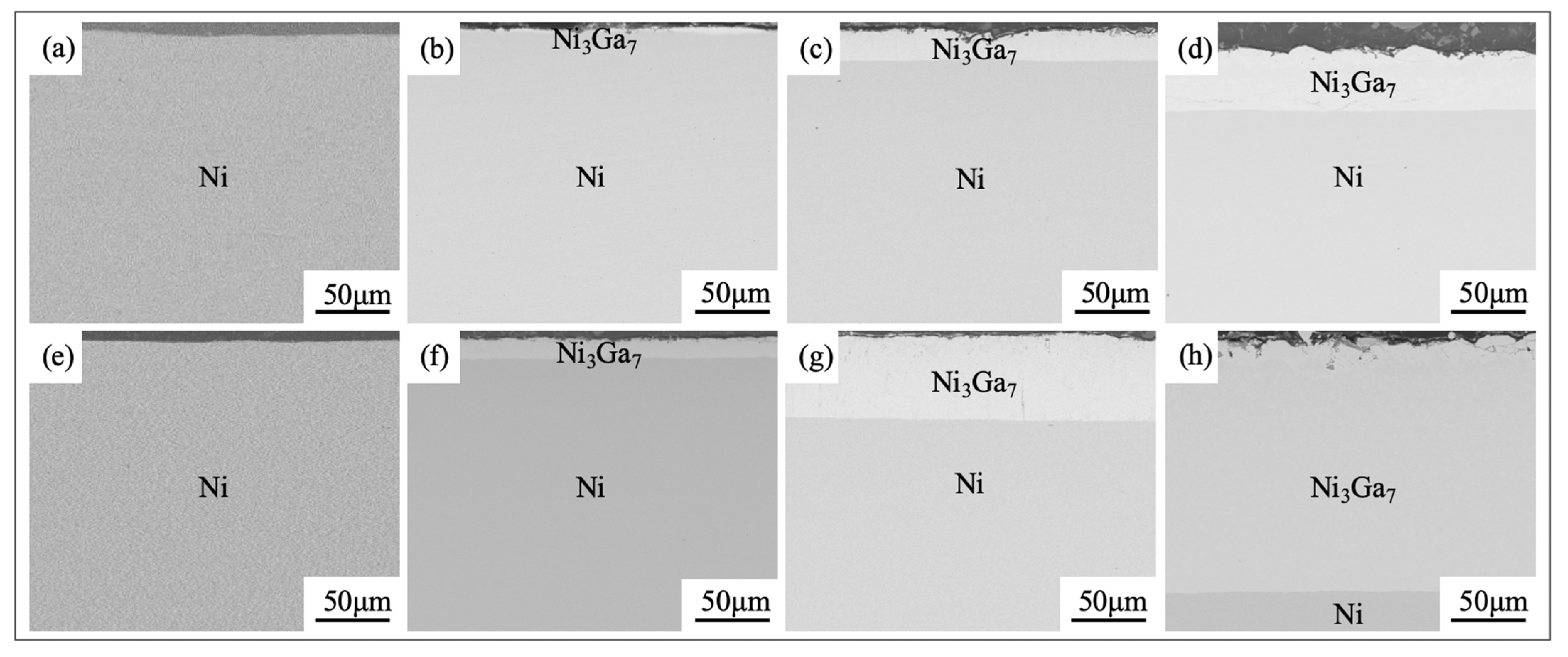
3.1. Microstructures and Phase Compositions

Figure 1 shows the interfacial morphology of the Ni/Ga diffusion couples in a cross-section view in backscattered electron mode. As shown in Figure 1a,e, only nickel substrate was observed in this layer at 323 K, and no obvious intermetallic compound was observed after annealing according to the scanning electron microscopy observation. According to the principle of backscattered electron imaging, the different brightness in the image reflects variations in atomic number; the brightness increases as the atomic number increases. Given that gallium (31) has a higher atomic number than nickel (28), the bright regions in Figure 1b–d,f–h are inferred to represent Ga-rich areas. Therefore, in each micrograph, the composition of the bright regions corresponds to an intermetallic compound, while that of the gray regions corresponds to Ni. The backscattered electron images in Figure 1b–h suggest that a single intermetallic compound reaction layer was formed in the Ni/Ga diffusion couple, and this became thicker as the temperature increased.
Figure 2 shows the cross-sectional backscattered electron image of a Ni/Ga diffusion couple reacted for 120 min at 623 K, as well as elemental mappings of Ga and Ni acquired via the electron probe micro-analyzer. To obtain detailed elemental distribution profiles, an EPMA line scan was performed along the region marked by arrows in Figure 2a. As shown in Figure 2b, the concentration of nickel approached 100 at. % in the gray region, whereas the concentration of gallium was close to 0 at. % in the same region. As the region transitions from bright to gray, the concentrations of gallium and nickel exhibit steep downward and upward trends, respectively. In the bright region, the concentrations of gallium and nickel remained relatively stable, indicating that no compositional gradient was observed. Based on the EPMA analysis, the composition of the intermetallic compound was determined as Ni-71.3 at. % Ga. Referring to the Ni-Ga phase diagram, it could be reasonably inferred that the planar intermetallic compound layer corresponds to the Ni3Ga7 phase. This is consistent with the findings of Chen et al. [6]. Due to the close atomic numbers of nickel and gallium, the backscattered electron image exhibits poor contrast between the Ni substrate and the Ni3Ga7 region. In the EPMA mappings (Figure 2c,d), the Ni substrate and Ni3Ga7 region are clearly distinguishable.
Intermetallic compounds are commonly observed in electronic joints. Although the formation of intermetallic compounds is usually accompanied by good wetting properties, the intermetallic compounds are electrically resistant. Meanwhile, electromigration and current crowding effects are more severe in miniaturized electronic solder joints. With increased temperature (from 423 K to 623 K) and annealing time (from 60 min to 480 min), the thickness of the Ni₃Ga₇ layer increased. Excess formation of Ni₃Ga₇ can reduce the electrical properties of electronic joints. Hence, optimizing the thickness of the Ni₃Ga₇ layer can be considered a method to improve the electrical properties of the interfacial region.

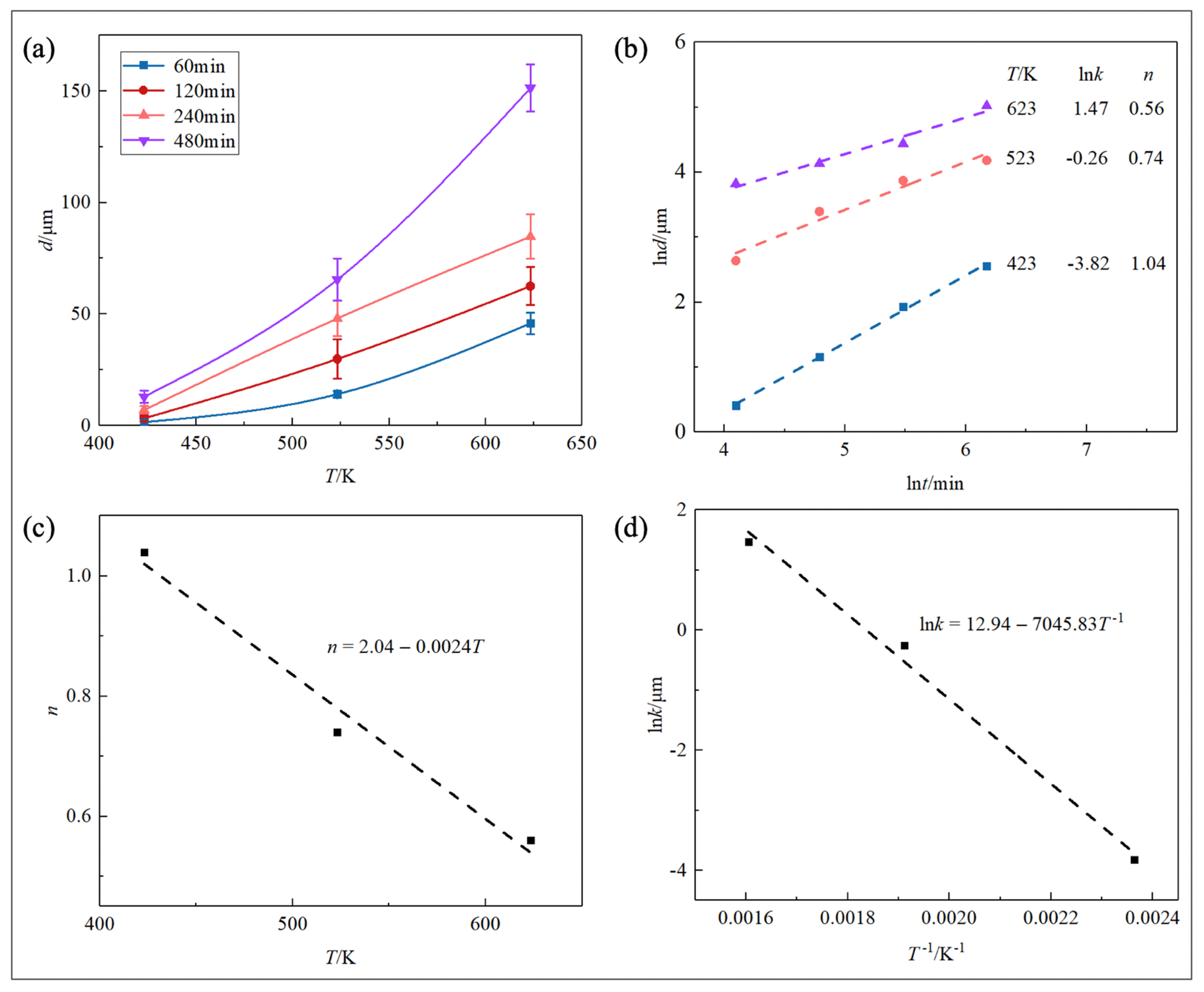
3.2. Diffusion Kinetics and Mechanism

Figure 3a presents the relationship between thickness of the intermetallic compound (d) and annealing temperature (T). As depicted in Figure 3a, the thickness of the intermetallic compound layer gradually increased with rising annealing temperature and prolonged annealing time.
The research by Schaefer et al. [20,21] demonstrates that the kinetics of phase formation during interfacial reaction diffusion are affected by morphological characteristics of the intermetallic compound layer. For systems where the characteristic morphology of the intermetallic compound layer is planar, the intermetallic compound growth during the interfacial reaction can be effectively modeled by the following empirical power-law model:
d = k × t n ,
where d is the average thickness of the intermetallic compound layer, k is the intermetallic compound growth rate constant, t is the annealing time, and n is the kinetic exponent. When the value of n is 1, the intermetallic compound growth is reaction-controlled, whereas when the value of n is 0.5, the intermetallic compound growth is volume diffusion-controlled [22]. When the thickness of the interfacial intermetallic compound layer is very thin, the intermetallic compound layer may not be continuous and flat, and the measurement of the real average intermetallic layer thickness becomes increasingly difficult. Therefore, the application of the power law is limited in cases of very thin layers.
Equation (1) can be transformed into the natural logarithmic form and written as follows:
ln d = ln k + n ln t
The relationship curve between lnt and lnd is plotted in Figure 3b. The linear fitting was applied to the experimental data, yielding the following results:
l n k = 3.82 ,   n = 1.04   for   T = 423   K ;
l n k = 0.26 ,   n = 0.74   for   T = 523   K ;
l n k = 1.47 ,   n = 0.56   for   T = 623   K
The kinetic exponent (n) obtained from the linear fitting was 1.04 for the reactions at 423 K, and Ni3Ga7 growth was controlled by reaction. Through linear regression analysis, the kinetic exponent was determined as 0.74 for the reactions at 523 K. Therefore, the growth of Ni3Ga7 during reaction diffusion was controlled by both reaction and volume diffusion. The kinetic exponent for Ni3Ga7 growth at 623 K was estimated to be 0.56, suggesting that the Ni3Ga7 growth was controlled by volume diffusion. Thus, the value of the time exponent (n) is not constant, and it is related to the annealing temperature. The variation of the time exponent with annealing temperature is shown in Figure 3c. From Figure 3c, it can be noted that the relationship between the time exponent and the annealing temperature is linear; the relationship is presented as Equation (3).
n = 2.04 0.0024 × T
The phase compositions, growth kinetics, and corresponding temperatures and times associated with each phase are summarized in Table 1. In general, the reaction diffusion is governed by two competing kinetic processes, namely, chemical reaction and atomic migration. At 423 K, the thickness of the Ni3Ga7 layer is linearly related to the time. This indicates that the growth rate of Ni3Ga7 phase was solely controlled by the chemical reaction rate at the growth site of the Ni3Ga7 phase, which means the growth of the Ni3Ga7 phase was not limited by the rate of the components’ diffusion to the reaction site. At this stage, the Ni3Ga7 phase had not yet formed a complete layered structure, and the diffusion of components was not a limiting factor, so the reaction rate determined the growth rate of Ni3Ga7 phase. At 623 K, the growth of Ni3Ga7 phase was clearly controlled by diffusion. This indicates that a relatively thick Ni3Ga7 layer had formed, and it took more time for components to diffuse to the reaction site. Therefore, the growth rate of the Ni3Ga7 phase was determined by the diffusion of components through the interfacial Ni3Ga7 layer to reach the reaction site, and the growth of the interfacial Ni3Ga7 phase followed a parabolic law. At 523 K, the growth of Ni3Ga7 phase during reaction diffusion was controlled by both reaction and volume diffusion. This can be understood as a synergy in which the reaction rate and the component diffusion rate jointly determine the growth rate of Ni3Ga7 phase.
The Arrhenius equation is as follows:
k = k 0 e x p ( Q R T )
Equation (4) can be manipulated into the natural logarithmic form and written as follows:
l n k = l n k 0 Q R T
As demonstrated in Figure 3d, linear fitting was conducted on the experimental data, which yielded the following results:
l n k 0 = 12.94 Q R = 7045.83
Thus:
k0 = 417174.55 μm Q = 58.58 kJ/mol
The activation energy (Q) for the Ni3Ga7 phase can be determined as 58.58 kJ/mol in the Ni/Ga system. Compared with the widely recognized Cu/Sn system [23], this value exceeds the activation energy (Q) for the growth of the ƞ-Cu6Sn5 phase (19.7 kJ/mol) but is lower than that for the ɛ-Cu3Sn phase (84.6 kJ/mol). Furthermore, according to Lin et al.’s report [24], the activation energy for the growth of the θ-CuGa2 layer in the Cu/Ga system can be calculated as 23.8 kJ/mol. The value of the activation energy is consistent with our calculation results in its order of magnitude.
The kinetics equation for Ni/Ga system can be expressed as follows:
d = 417174.55 exp 58579 R T t 2.04 0.0024 T
Importantly, the obtained kinetics equation and the reactants in Ni/Ga system were also verified. According to the kinetics equation of the Ni/Ga diffusion couple, the thicknesses of interfacial Ni3Ga7 at 323 K for 60 min and 480 min were calculated to be 0.024 μm and 0.33 μm, respectively. These thicknesses are so tiny that the Ni3Ga7 layer could not be observed with scanning electron microscopy. Thus, as mentioned above, at temperatures lower than 323 K, no obvious intermetallic compound was identified after annealing.
Ni is commonly used as a barrier layer in electronic devices, while Cu serves as a popular electrode material. Hence, it is necessary to compare the reaction diffusion behaviors in Ni/Ga systems and those in Cu/Ga systems. In a Cu/Ga system [24], the kinetic exponent (n) is 1.00 for reactions at 433 K, indicating that the growth is likely to be controlled by reaction. At 473 K, the value of n is 0.50, indicating a volume-diffusion-controlled mechanism. For reactions at 553 K, the kinetic exponent (n) of the power law is 0.36. This value is close to 0.33, suggesting that the reaction is likely to be dominated by grain-boundary diffusion. In summary, at lower reaction temperatures, growth of the intermetallic compound is probably determined by the reaction. However, it becomes volume-diffusion-controlled at higher temperatures. The comparative analysis of activation energy (Q) revealed that the Ni/Ga system exhibited significantly higher Q values than the Cu/Ga system. It is reasonable that the activation energy of the Ni/Ga diffusion couple should be higher than that of Cu/Ga, because the melting point of Ni is much higher than that of Cu. The higher melting point makes atomic diffusion much more difficult. Generally, the higher the activation energy, the slower is the formation rate of the intermetallic compounds.
It is well known that the presence of intermetallic compounds between solder alloys and the substrate is an indication and essential requirement of good metallurgical bonding. Therefore, the formation of the Ni3Ga7 phase during interfacial reaction diffusion suggests that Ga is a good candidate for bonding Ni substrates in solid–liquid interdiffusion bonding processes for the preparation of flexible electronic devices.
The reliability of electronic packaging has always been a research hotspot. This issue becomes more complex as the solder joint changes from a large solder joint to a small solder joint. With the miniaturization of solder joints, the relative proportion of the intermetallic compound layer in the total joint volume increases. In some cases, the intermetallic compounds make up the entire joint. For Ga-based low-temperature soldering, after the soldering reactions are complete, the joint is typically filled with intermetallic compounds to ensure a reasonable operating temperature during service. Intermetallic compounds in solder joints play an important role in joint reliability and influence failure mechanisms. Thus, the growth kinetics of Ni3Ga7 significantly impact the reliability of low-temperature soldering between Ga and Ni substrates.
Moreover, the mechanical and physical properties of the Ni3Ga7 phase substantially differ from those of the solder and substrate. An excessively thick Ni3Ga7 layer could degrade the reliability of the solder joints due to the inherent brittleness of the Ni3Ga7 phase and its tendency to generate structural defects such as volume shrinkage and Kirkendall voids associated with Ni3Ga7 phase formation. The most common cause of void formation in solid–liquid interdiffusion bonding systems is volume shrinkage. When the two initial reacting elements react to form an intermetallic compound layer, in most cases, the volume of the joint shrinks. Kirkendall voids form and grow in the solder joint as a result of different interdiffusion rates within intermetallic compounds at the interface between the solder and the metal bond-pad during soldering. Because of the detrimental effects of voids on the mechanical and thermal integrity of the solder joint, this phenomenon must be prevented or reduced. Therefore, avoiding excessive growth of the Ni3Ga7 phase in the solder interconnects is extremely important to ensure the reliability of the solder interconnects. The processing conditions, such as bonding temperature and bonding time, need to be optimized to control the growth of Ni3Ga7. This will help reduce voids in intermetallic compound solder joints and improve the reliability of electronic packaging.
In addition, in flexible electronics applications, it may be desirable to either enhance or minimize the formation of Ni3Ga7 as this will affect functionality such as wettability or electrical conductivity.
Overall, based on the kinetics equation for the Ni/Ga system, the thickness of the intermetallic compound layer at any time during the reaction diffusion process can be predicted. Thus, this method can be applied in industrial solid–liquid interdiffusion bonding processes to enhance the reliability and lifetime of solder joints by allowing control of the thickness of intermetallic layers.

4. Conclusions

Microstructural characterization of the Ni/Ga diffusion couple indicated that no obvious intermetallic compound was observed at temperatures lower than 323 K. For reactions at 423 K, 523 K, and 623 K, the Ni3Ga7 phase was the only reaction product. The time exponents for Ni3Ga7 growth were estimated to be 1.04, 0.74, and 0.56 at 423 K, 523 K, and 623 K, respectively. The activation energy for the growth of Ni3Ga7 in the Ni/Ga system was determined as 58.58 kJ/mol. The kinetics equation for Ni/Ga system can be expressed as follows: d = 417174.55 exp 58579 R T t 2.04 0.0024 T . The research results of this study have implications for the broad utilization of Ga-based alloys in microelectronics. In addition, the reliability of real Ga-based Ni-to-Ni (or other metal substrate) three-dimensional integrated packaging joints requires further study.

Author Contributions

Conceptualization, T.W.; methodology, J.P.; software, J.P.; validation, T.W. and S.Z.; formal analysis, J.P.; investigation, J.P.; resources, T.W. and S.Z.; data curation, J.P.; writing—original draft preparation, J.P.; writing—review and editing, T.W.; visualization, J.P.; supervision, T.W. and S.Z.; project administration, T.W. and S.Z.; funding acquisition, T.W. and S.Z. All authors have read and agreed to the published version of the manuscript.

Funding

This research received no external funding.

Data Availability Statement

Data are contained within the article.

Conflicts of Interest

The authors declare no conflicts of interest.

References

  1. Chen, S.; Wang, H.Z.; Zhao, R.Q.; Rao, W.; Liu, J. Liquid Metal Composites. Matter 2020, 2, 1446–1480. [Google Scholar] [CrossRef]
  2. Dickey, M.D.; Chiechi, R.C.; Larsen, R.J.; Weiss, E.A.; Weitz, D.A.; Whitesides, G.M. Eutectic Gallium-Indium (EGaIn): A Liquid Metal Alloy for the Formation of Stable Structures in Microchannels at Room Temperature. Adv. Funct. Mater. 2008, 18, 1097–1104. [Google Scholar] [CrossRef]
  3. Kim, M.; Park, J.J.; Cho, C.; Ko, S.H. Liquid Metal based Stretchable Room Temperature Soldering Sticker Patch for Stretchable Electronics Integration. Adv. Funct. Mater. 2023, 33, 2003286. [Google Scholar] [CrossRef]
  4. Chen, S.W.; Lin, J.M.; Yang, T.C.; Du, Y.H. Interfacial Reactions in the Cu/Ga/Co and Cu/Ga/Ni Samples. J. Electron. Mater. 2019, 48, 3643–3653. [Google Scholar] [CrossRef]
  5. Daalkhaijav, U.; Yirmibesoglu, O.D.; Walker, S.; Menguc, Y. Rheological Modification of Liquid Metal for Additive Manufacturing of Stretchable Electronics. Adv. Mater. Technol. 2018, 3, 1700351. [Google Scholar] [CrossRef]
  6. Ozutemiz, K.B.; Wissman, J.; Ozdoganlar, O.B.; Majidi, C. EGaIn−Metal Interfacing for Liquid Metal Circuitry and Microelectronics Integration. Adv. Mater. Interfaces 2018, 5, 1701596. [Google Scholar] [CrossRef]
  7. Jiang, M.Z.; Chen, S.; Zhang, P.; Sun, Y.W.; Ye, J.; Deng, Y.Q.; Li, L.; Liu, J. Liquid metal enabled plant injectable electronics. Mater. Today 2023, 66, 50–61. [Google Scholar] [CrossRef]
  8. Yuan, R.Z.; Cao, Y.J.; Zhu, X.Y.; Shan, X.H.; Wang, B.; Wang, H.Z.; Chen, S.; Liu, J. Liquid Metal Memory. Adv. Mate. 2024, 36, 2309182. [Google Scholar] [CrossRef]
  9. Ma, X.H.; Wu, X.T.; Cao, S.T.; Zhao, Y.F.; Lin, Y.; Xu, Y.R.; Ning, X.H.; Kong, D.S. Stretchable and Skin-Attachable Electronic Device for Remotely Controlled Wearable Cancer Therapy. Adv. Sci. 2023, 10, 2205343. [Google Scholar] [CrossRef]
  10. Deng, Y.G.; Liu, J. Corrosion development between liquid gallium and four typical metal substrates used in chip cooling device. Appl. Phys. A 2009, 95, 907–915. [Google Scholar] [CrossRef]
  11. Ralphs, M.; Kong, W.; Wang, R.Y.; Rykaczewski, K. Thermal Conductivity Enhancement of Soft Polymer Composites through Magnetically Induced Percolation and Particle–Particle Contact Engineering. Adv. Mater. Interfaces 2019, 6, 1801857. [Google Scholar] [CrossRef]
  12. Lin, S.K.; Wang, M.J.; Yeh, C.Y.; Chang, H.M.; Liu, Y.C. High-strength and thermal stable Cu-to-Cu joint fabricated with transient molten Ga and Ni under-bump-metallurgy. J. Alloy. Compd. 2017, 702, 561–567. [Google Scholar] [CrossRef]
  13. Laurila, T.; Vuorinen, V.; Kivilahti, J.K. Interfacial reactions between lead-free solders and common base materials. Mat. Sci. Eng. R. 2005, 49, 1–60. [Google Scholar] [CrossRef]
  14. Laurila, T.; Vuorinen, V.; Paulasto-Krockel, M. Impurity and alloying effects on interfacial reaction layers in Pb-free soldering. Mat. Sci. Eng. R. 2010, 68, 1–38. [Google Scholar] [CrossRef]
  15. Lin, S.K.; Chang, H.M.; Cho, C.L.; Liu, Y.C.; Kuo, Y.K. Formation of solid-solution Cu-to-Cu joints using Ga solder and Pt under bump metallurgy for three-dimensional integrated circuits. Electron. Mater. Lett. 2015, 11, 687–694. [Google Scholar] [CrossRef]
  16. Mikheev, A.A.; Temnykh, V.I.; Kazakov, V.S.; Temnykh, E.V.; Mityaev, A.E.; Zeer, G.M.; Abkaryan, A.K. Kinetics and Products of Interaction of Zinc-Containing Gallium Pastes-Solders. Welding Int. 2012, 36, 314–315. [Google Scholar] [CrossRef]
  17. Chen, C.H.; Lee, B.H.; Chen, H.C.; Wang, C.M.; Wu, A.T. Interfacial Reactions of Low-Melting Sn-Bi-Ga Solder Alloy on Cu Substrate. J. Electron. Mater. 2016, 45, 197–202. [Google Scholar] [CrossRef]
  18. Froemel, J.; Baum, M.; Wiemer, M.; Gessner, T. Low-Temperature Wafer Bonding Using Solid-Liquid Inter-Diffusion Mechanism. J. Microelectromech. S. 2015, 24, 1973–1980. [Google Scholar] [CrossRef]
  19. Liu, S.Q.; Tan, X.F.; McDonald, S.D.; Gu, Q.F.; Matsumura, S.; Nogita, K. Interfacial reactions between Ga and Cu-xNi (x = 0, 2, 6, 10, 14) substrates and the strength of Cu-xNi/Ga/Cu-xNi joints. Intermetallics 2021, 133, 107168. [Google Scholar] [CrossRef]
  20. Schaefer, M.; Laub, W.; Sabee, J.M.; Fournelle, R.A. A Numerical Method for Predicting Intermetallic Layer Thickness Developed During the Formation of Solder Joints. J. Electron. Mater. 1996, 25, 992–1003. [Google Scholar] [CrossRef]
  21. Schaefer, M.; Fournelle, R.A.; Liang, J. Theory for Intermetallic Phase Growth Between Cu and Liquid Sn-Pb Solder Based on Grain Boundary Diffusion Control. J. Electron. Mater. 1998, 27, 1167–1176. [Google Scholar] [CrossRef]
  22. Liu, S.Q.; Zeng, G.; Yang, W.H.; McDonald, S.; Gu, Q.F.; Matsumura, S.; Nogita, K. Interfacial Reactions between Ga and Cu-10Ni Substrate at Low Temperature. ACS Appl. Mater. Interfaces 2020, 12, 21045–21056. [Google Scholar] [CrossRef] [PubMed]
  23. Li, J.F.; Agyakwa, P.A.; Johnson, C.M. Interfacial reaction in Cu/Sn/Cu system during the transient liquid phase soldering process. Acta Mater. 2011, 59, 1198–1221. [Google Scholar] [CrossRef]
  24. Lin, S.K.; Cho, C.L.; Chang, H.M. Interfacial reactions in Cu/Ga and Cu/Ga/Cu couples. J. Electron. Mater. 2014, 43, 204–211. [Google Scholar] [CrossRef]
Figure 1. Backscattered electron images of Ni/Ga diffusion couples reacted for (a) 60 min at 323 K, (b) 60 min at 423 K, (c) 60 min at 523 K, (d) 60 min at 623 K (e) 480 min at 323 K, (f) 480 min at 423 K, (g) 480 min at 523 K, (h) 480 min at 623 K.
Crystals 15 00520 g001
Figure 2. (a) The backscattered electron image of a Ni/Ga couple reacted for 120 min at 623 K; (b) EPMA compositional line-scan; (c) EPMA elemental mapping of Ga; (d) EPMA elemental mapping of Ni.
Crystals 15 00520 g002
Figure 3. (a) The relationship curve between the thickness of the Ni₃Ga₇ layer and annealing temperature; (b) lnt—lnd; (c) the relationship curve between the time exponent and annealing temperature; (d) T−1—lnk.
Crystals 15 00520 g003
Table 1. The phase compositions and growth kinetics at different temperatures and times.
Temperature (K)Time (min)Reaction Phasekinetic Exponent (n)
42360Ni3Ga71.04
120Ni3Ga71.04
240Ni3Ga71.04
480Ni3Ga71.04
52360Ni3Ga70.74
120Ni3Ga70.74
240Ni3Ga70.74
480Ni3Ga70.74
62360Ni3Ga70.56
120Ni3Ga70.56
240Ni3Ga70.56
480Ni3Ga70.56
Disclaimer/Publisher’s Note: The statements, opinions and data contained in all publications are solely those of the individual author(s) and contributor(s) and not of MDPI and/or the editor(s). MDPI and/or the editor(s) disclaim responsibility for any injury to people or property resulting from any ideas, methods, instructions or products referred to in the content.

