Article

Inspection of Bulk Crystals for Quality Control in Crystal Growth: Assessment of High-Energy X-Ray Transmission Topography and Back-Reflection Topography Pinpointed for Physical Vapor Transport-Grown Aluminum Nitride

1
Fraunhofer Institute for Integrated Systems and Device Technology IISB, Department Materials, Schottkystraße 10, 91058 Erlangen, Germany
2
Institute for Crystallography and Structural Physics, Friedrich-Alexander-Universität Erlangen-Nürnberg, Staudtstraße 3, 91058 Erlangen, Germany
*
Author to whom correspondence should be addressed.
Crystals 2025, 15(5), 449; https://doi.org/10.3390/cryst15050449
Submission received: 27 March 2025 / Revised: 5 May 2025 / Accepted: 6 May 2025 / Published: 9 May 2025
(This article belongs to the Section Crystal Engineering)

Abstract

:
A comprehensive X-ray topography analysis of two selected aluminum nitride (AlN) bulk crystals is presented. We compare surface inspection X-ray topography in back-reflection geometry with high-energy transmission topography in the Lang and Laue configuration using the monochromatic Kα1 excitation wavelength of copper, silver, and tungsten, respectively. A detailed comparison of the results allows the assessment of both the high- and low-energy X-ray topography methods with respect to performance and structural information, giving essential feedback for crystal growth. This is demonstrated for two selected AlN freestanding faceted crystals up to 8 mm in thickness grown in all directions using the physical vapor transport (PVT) method. Structural defects of all facets of the crystals are determined using the X-ray topography in back-reflection geometry. The mean threading dislocation densities are 480 ± 30 cm−2 for both crystals of either the Al- or N-face. Clustering of dislocations could be observed. The m-facets show the presence of basal plane dislocations and their accumulation as clusters. The integral transmission topographs of the 10 1 ¯ 0 (m-plane) reflection family show that basal plane dislocations of the screw type in 1 3 1 ¯ 2 1 ¯ 0 directions decorate threading dislocation clusters. Three-dimensional section transmission topography reveals that the basal plane dislocation clusters mainly originate at the seed boundary and propagate in the 1 3 1 ¯ 2 1 ¯ 0 direction along the growth front. In newly laterally grown material, the Borrmann effect has been observed for the first time in PVT-grown bulk AlN, indicating very high structural perfection of the crystalline material in this region. This agrees with a low mean FWHM of 10.6 arcsec of the 10 1 ¯ 0 reflection determined through focused high-energy Laue transmission mappings. The latter method also opens the analysis of the 2 θ -shift correlated to the residual stress distribution inside the bulk crystal, which is dominated by dislocation clusters. Contrary to Lang transmission topography, the de-focused high-energy Laue transmission penetrates the 8 mm-thick crystal enabling a defect analysis in the bulk.

1. Introduction

Aluminum nitride (AlN) is a promising ultra-wide-bandgap semiconductor (UWBG) suitable for optoelectronic, power electronic, and high-frequency applications [1,2]. Two-inch wafers with low dislocation densities of 102 to 104 cm−2 are nowadays commercially available. Strong efforts towards larger diameters are in progress to gain higher industrial attractiveness and maturity [3,4]. The crystals are typically grown using the sublimation growth method (PVT), similar to silicon carbide [5,6,7]. According to the specific application, the crystals are either grown on the N- or Al-face of the AlN seed, giving rise to different carbon concentrations. For example, the material produced using the latter method typically shows a lower carbon concentration and thus is more suitable for UVC-LEDs [8]. Independent of the growth method, any diameter increase must not be at the expense of an increasing defectivity of the material, especially in terms of dislocations and other macroscopic defects [9]. Thus, a detailed structural characterization of the bulk material, proper seed selection, and a consequent feedback loop for optimizing crystal quality, growth, and the expansion process is essential. It is especially desirable to have tools at hand for the characterization of the full bulk crystal before wafering to provide a complete picture of the dislocation network and its genesis. Particularly, the formation of dislocations at the seed-to-crystal interface is of high interest because it allows the grower to judge the quality of the seeding procedure and the very first stage of the growth process. To obtain the requested structural information, X-ray topography serves as a well-known standard characterization method [7,10,11]. One major benefit compared to other methods, like transmission electron microscopy, is that it is non-destructive with no need for further preparation of the sample. However, methods for X-ray topography are numerous, and each of them has its advantages and disadvantages with respect to the structural characterization of bulk crystals. Although X-ray topography investigations for AlN wafers utilizing synchrotron radiation [12,13,14,15,16] and recently also with laboratory scale X-ray setups [17] have been reported, little is demonstrated yet on full as-grown bulk crystals [18].
It is a key focus of this work to present suitable laboratory scale X-ray topography methods and assess their potential for structural bulk crystal characterization using the UWBG material AlN as a specific example. In comparison to superior synchrotron techniques, the methods discussed here have the advantage of easy use and access at moderate costs and provide sufficient high image quality to draw technological and scientific conclusions in the achievement of the purpose of this study. As a featured application, we show how these methods can act as a tool for the structural quality control of as-grown bulk crystals and as feedback for crystal growth without the need for wafering. We emphasize that this investigation can be applied to other materials of interest.
According to the penetration depth into the material and to the crystal thickness, we classify our X-ray topography methods into the classes surface inspection and bulk inspection (see Figure 1). The former is realized in back-reflection geometry using the monochromatic Kα1 line of a copper anode, while the latter is performed in Lang transmission geometry using a silver anode. In case of relatively thick crystals (i.e., >5 mm), a Laue setup with a tungsten anode is used instead, since the penetration of X-rays at the characteristic line of silver does not give sufficient transmitted intensity.
The surface inspection method gives structural information about dislocations close to the surface within the given penetration depth. Contrary to wafers after slicing and even polishing, the as-grown surfaces of bulk crystals do not exhibit any residual surface damages that could perturb the measured dislocations’ contrast. Other inhomogeneities, like lattice distortion or surface warp, can be corrected within the measurement procedures. Typically, threading dislocations appear as distorted dark spots in X-ray topographs of the Al- or N-face, and their number determines the dislocation density equivalent to the already demonstrated methodology for commercial 4H-SiC or GaN wafers [19,20,21]. Also, macroscopic defects, such as grain boundaries and dislocation clusters, can be detected. Assessments of basal plane dislocations can be performed, when side facets of the crystal are investigated in surface inspection mode. However, it is obvious that no direct insight into the defect content within the bulk of the crystal can be gained from the surface inspection. To overcome this, topography in transmission geometry was used.
Topographs carried out in Lang transmission contain integrated information about the whole crystal thickness such that interpretation for crystals with high dislocation densities becomes cumbersome. Dislocation networks of crystals with densities below 1000 cm−2 and thicknesses smaller than 10 mm can be resolved with sufficient quality [22]. For thick crystals (>5 mm), the X-rays of a Laue setup with a tungsten anode can penetrate the crystal even in the lateral direction. In addition, the Laue reflection in focused mode gives energy dispersive information, i.e., information about global stress and the crystal quality through a rocking curve analysis [23,24]. Using a micro-slit in the incident beam, the excitation volume is confined within a small slice of the crystal. With subsequent spatial mappings, a three-dimensional topography model of the crystal can be derived (section topography) [25]. The spatial distribution of the dislocation network is visible, and the origin of dislocation generation can be exposed.
In the next section, we describe, shortly, the growth setup for AlN bulk growth and present a detailed description of the surface and bulk inspection methods. Then, we proceed with the description of two selected crystals, i.e., presenting their growth history, characterizing their surface facets and lattice distortion.
We start the result section with the presentation of the topographs in back-reflection geometry of all facets for two crystals. The topographs of the N- and Al- faces are used for a determination of the threading dislocation densities and a visualization of the dislocation distribution, which also addresses their clustering. In continuation, the integral Lang transmission topographs taken based on m- and a-plane reflections are presented. Special attention is provided for the basal plane dislocations around threading dislocation clusters. A Burgers vector analysis shows that the majority has a screw component. Additionally, dislocation clusters onto the basal plane in the diameter expansion region are in the crystallographic orientation at the m-facet. A comparison of the topographs with the seed shape suggested that they are generated at the seed boundaries following the growth front. The latter can be confirmed via section topography, and the presence of a c-component of the line vector is proven. The analysis of the Laue reflection in focused mode provides a mapping of the tensile and compressive stress in the crystals, which correlates to the asymmetric growth front close to adjacent m-facets.

2. Materials and Methods

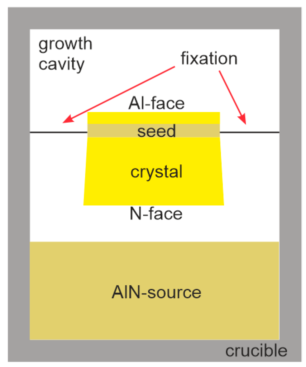
2.1. Aluminum Nitride PVT Growth

Bulk crystals of AlN were grown in our laboratory at IISB using the physical vapor transport method (PVT) [17]. Figure 2 schematically shows the core of the growth setup. Inside a crucible, an AlN seed wafer is placed with the N-face down in a floating position laterally fixed at the periphery. AlN powder is located at the bottom of the crucible and serves as a source material, which has been purified beforehand via re-sublimation in an external carbon-free reactor. The setup is held under a nitrogen pressure of 700 to 900 mbar.
When a temperature of approximately 2500 K is reached, the source material starts to sublime and re-condensates at the seed, which has a lower temperature. The setup leads to low radial and axial temperature gradients. Together with the floating seed fixation scheme, bulk growth close to equilibrium is achieved and growth of the N-face dominates. With growth rates between 30 and 120 µm/h, mainly driven by the axial temperature gradient, and growth times from 60 to 100 h, crystals are typically approximately 2 to 9 mm in height. The diameter of the crystal is determined by the size of the seed and is increased through lateral growth.
In this publication, we present comprehensive characterization results from X-ray techniques performed on two bulk crystals, referenced as crystal A and crystal B. Both crystals have been grown on adjacent seed wafers from the same boule. The growth conditions (see Table 1) were kept as close as possible, except for the temperature gradient, which is about three times higher in sample B, leading to a larger crystal thickness and to different defect development, which is part of a later discussion. While all methods presented in this work can be applied to crystal A, the bulk inspection of crystal B can be performed only with the Laue transmission setup. In addition, crystal B shows a larger content of dislocation clusters illustrating the capability and limits of the X-ray characterization techniques presented in this work.

2.2. Experimental Measurement Setups

2.2.1. Surface Inspection Tool

The surface shape and orientation of our crystals are characterized using an SDCOM from Freiberg Instruments GmbH, Freiberg, Germany. It can simultaneously determine the surface and lattice topography of the crystal through laser reflection and X-ray diffraction, respectively. While rotating the sample, a laser with a spot size smaller than 1 mm is reflected at the surface and detected by a camera. The resulting trajectory of the reflected laser signal contains, locally, the surface tilt information of the sample with respect to the instrumental setup. During the same sample rotation, the diffracted X-ray beam with a spot diameter smaller than 2 mm is recorded. The dependency of the X-ray signal on the sample rotation gives the lattice tilt with respect to the setup. By mapping the complete sample surface with a squared grid spacing of 2 mm, the surface topography and lattice shape can be calculated and visualized.
For samples with a highly unsmooth, rough, or curved surface, the laser reflection is not or only partially measurable. Nevertheless, this does not affect the X-ray measurements. Lattice curvature data are extracted by fitting a reference plane into the lattice-height data and subtracting this plane from the data.

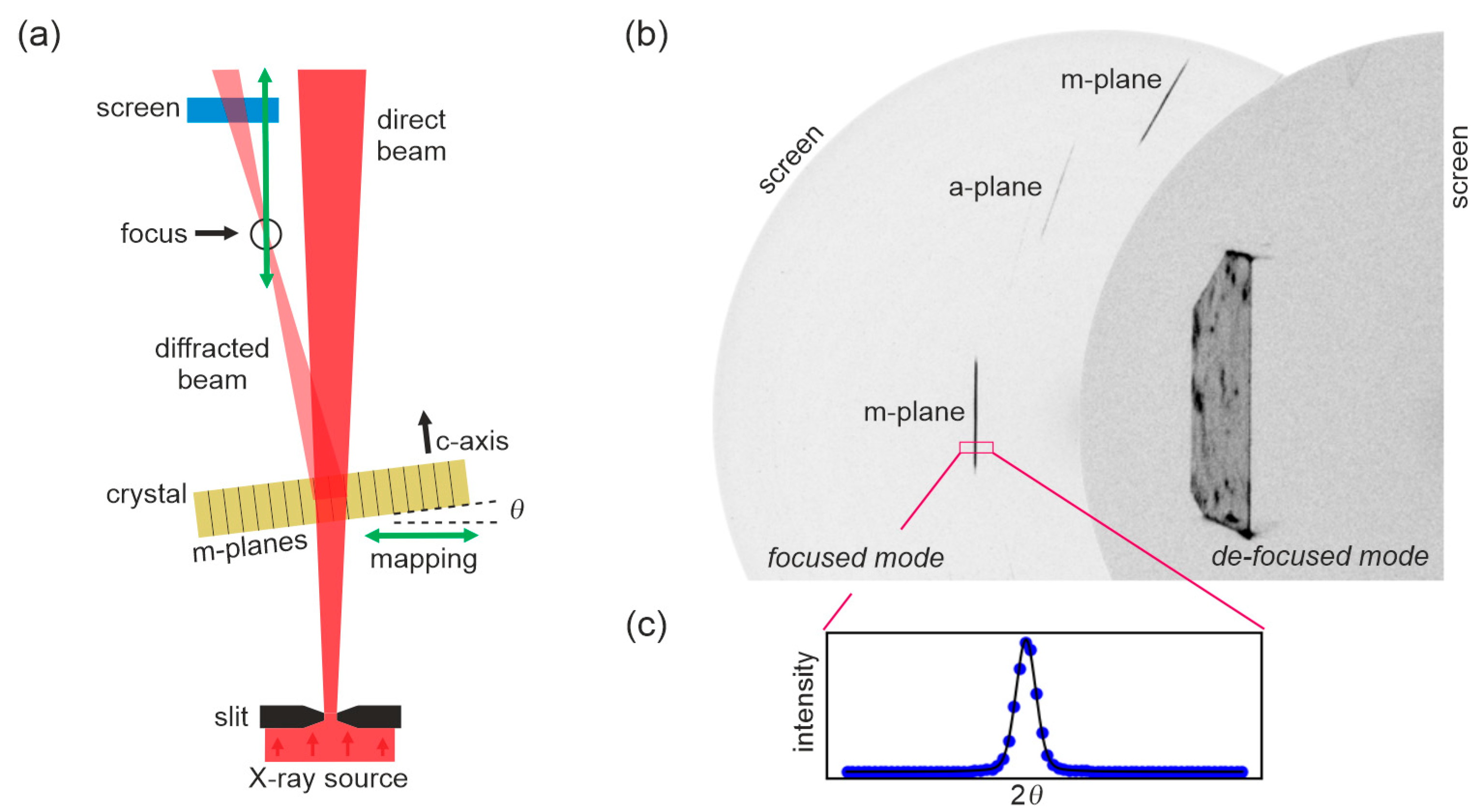
2.2.2. X-Ray Topography Setups (Back-Reflection and Lang Transmission)

For the X-ray topography measurements, two setups of XRTmicron from Rigaku Holdings Corporation, Tokyo, Japan were utilized at IISB. Both have identical goniometer and detector settings and differ only in the material of the high-brilliance rotating anode of the X-ray source. In this work, we use copper, molybdenum, and silver as anode material leading to characteristic wavelengths suitable for measurements in either transmission or back-reflection geometry (see Table 2 and Figure 1).
The size of the micro-focus on the rotating anodes is similar for all anode materials and is in the range of 70 to 150 µm. A photomultiplier with a scintillator counter serves as the detector for the alignment procedure, whereas a high-sensitivity and high-resolution camera, model XTOP, with 3300 × 2526 pixels of 5.4 × 5.4 µm2 in size serves as the area detector for the topography measurements. A parabolic multi-layered mirror parallelizes the beam within the goniometer plane (x-z plane) with beam divergency of ~0.3 mrad, while the divergency perpendicular to the goniometer plane (x-y plane) is approximately two orders of magnitudes higher, i.e., ~100 mrad, and is determined by the aperture of the X-ray source window alone. The sample is placed on a rotatable x-y-stage with a Kapton® foil [28] ensuring negligible absorption of X-rays when operating in transmission mode. The sample holder has no goniometer stage, and the source and detector goniometer planes are fixed to the laboratory frame. In the case of section topography, a micro-slit of 37 µm placed in the incident beam confines the excitation volume within the crystal to a small vertical slice.

2.2.3. High Energy X-Ray Laue Topography Setup

The setup for high-energy Laue topography, HexBay, was built at ICSP (for a schematic drawing, see Figure 3a and [23,24]). The X-ray source consists of a tungsten anode, which operates up to 225 kV at 630 W. The size of the focus is 400 µm. The sample is mounted on an x-y-goniometer in the horizontal plane with a rotatable stage for setting the diffraction angle. The distance of the samples is set at 3 m from the source, and the detector can be positioned at the same distance in the focusing condition or up to 12 m in the de-focused condition. The slit/collimator ensemble provides a rectangular beam shape up to 10 mm in width and 20 mm in height illuminating the complete crystal in de-focused mode. An image plate detector mar345 from marXperts GmbH, Norderstedt, Germany is used with a pixel size of 100 × 100 µm2 and detector size of 345 mm in diameter. In this arrangement, diffraction angles between 0.2° to 15° are accessible.

2.3. X-Ray Measurement Procedures

The measurement procedure for the reflection and transmission measurements using the XRTmicron follows a three-step procedure, which is described in detail in Appendix A. Schematic drawings of the measurement modes are presented in Figure 4.

2.3.1. X-Ray Topography in Reflection Geometry

The surface inspection of the bulk crystals is performed based on X-ray topography in reflection geometry with the XRTmicron tool (see Figure 4a). Together with the technical limitations of the goniometer settings and the surface orientation of the sample a restricted set of reflections is accessible only. In this work, we restricted our investigation on the reflections given in Table 3, which cover the measurements of all observed facets in symmetric back-reflection geometry.

2.3.2. X-Ray Topography in Transmission Geometry (Lang)

Bulk inspection is performed by using a-plane and m-plane reflections via Lang transmission topography (see Figure 4b). If a Burgers vector analysis of basal plane dislocations is required, adjacent m-planes (0°, 60° and 120°) are selected and respective topographs are measured. Since the sample thickness of the crystals is up to 8 mm, X-ray absorption plays a crucial role. In Table 1, the absorption coefficients and respective penetration depths of AlN for the characteristic Kα1 wavelengths used in our setups are given. Although the linear absorption coefficient does not reflect the true absorption in the Bragg condition, it can nevertheless give an approximation. We do not expect anomalous absorption, as the μ t values for our crystals are below ten. Therefore, it is obvious that the copper anode cannot be used for transmission measurements. The penetration depth using the silver anode is sufficiently high to measure crystal A, at least with a large exposure time (scan time > 20 h), but it fails for crystal B, which has twice the thickness of crystal A. However, the latter is measurable with a tungsten anode, which offers the largest X-ray energy of our setups.

2.3.3. High-Energy Laue Topography in Transmission Geometry

The setup in Figure 3a was already described in Chapter 2.2.3. The bulk is mounted on the m- or a-plane such that the c-axis points towards the source under an angle in the order of the Bragg angle of the m- or a-plane (see Table 3). Positioning the detector in the focused condition, i.e., detector to sample distance equals the sample to source distance, a typical Laue diffraction pattern is visible (see Figure 3b, left). The alignment of the goniometer, detector position, and diffraction angles are chosen such that a single reflection on the screen is aligned vertically. This reflection spot delivers no spatial resolution in the x-direction but information about local mosaicity (line broadening) and angular deviation from a mean Bragg angle (peak shift). However, the in y-direction, the position sensitivity can easily be obtained. With a slit width of 500 µm and focus distance of 3 m, the area illuminated by X-rays on the crystal is confined by the 2.6 mm in the x-direction, whereas in the y-direction, it is limited by the size of the crystal alone. In contrast to the focused Laue reflection spot, the de-focused spot delivers spatial resolution in the x-direction as in the y-direction. Thus, a qualitative overview about the defect structure of the illuminated crystal volume can be received in one shot.
To obtain a complete quantitative map of the crystal, Laue reflections at a series of x-positions in steps of 1 mm are recorded. The intensity profile of one row of the Laue reflection is the equivalent to a rocking curve as shown in Figure 3c. The Gaussian profile is evident. However, best fits are obtained using a Pseudo-Voigtian peak shape, i.e., mixing of Lorentzian with Gaussian, for all line profiles of all Laue reflection spots:
I 2 θ I 0 = η · 1 1 + 2 θ 2 θ 0 FWHM 2 + 1 η · exp 4 log 2 2 θ 2 θ 0 FWHM 2
Four fitting parameters as a function of the wafer positions are obtained in this way: the maximum intensity of the peak I 0 , the full-width half maximum FWHM, the 2 θ -peak-position 2 θ 0 and the mixing parameter η giving rise to respective contour plots. The thickness broadening of the FWHM by the factor 2 d sin θ has been considered.

2.3.4. Three-Dimensional Section Topography

The experimental arrangement of the section topography method is the same as for the transmission measurement with the exception that after the standard alignment procedure (described in Appendix A), a micro-slit of 37 µm is used (see Figure 4c). A small slice of the crystal is penetrated by the X-rays at the Bragg angle of the m-plane, and the diffracted beam of this slice is recorded at the detector containing the depth information of dislocations within this slice. In order to obtain a three-dimensional picture, stepping of the stage in the x-direction and recording a series of slices are necessary. To obtain continuous information about the dislocation content between the slices, it is convenient to choose the stepping distance in the order of the slit width. In our section measurements, we have chosen a separation of 40 µm between the slices and then recorded 750 slices to cover 30 mm of the crystal in the x-direction. The 3D model shown in the animated Video S1 (Supplementary Materials) and in Figure 11 is obtained by re-slicing the stack of section topographs in the c-direction. This re-slicing procedure needs to consider the off-alignment from the c-axis of each slice due to the Bragg angle and the perspective distortion of the slice image on the camera.

3. Results and Discussion

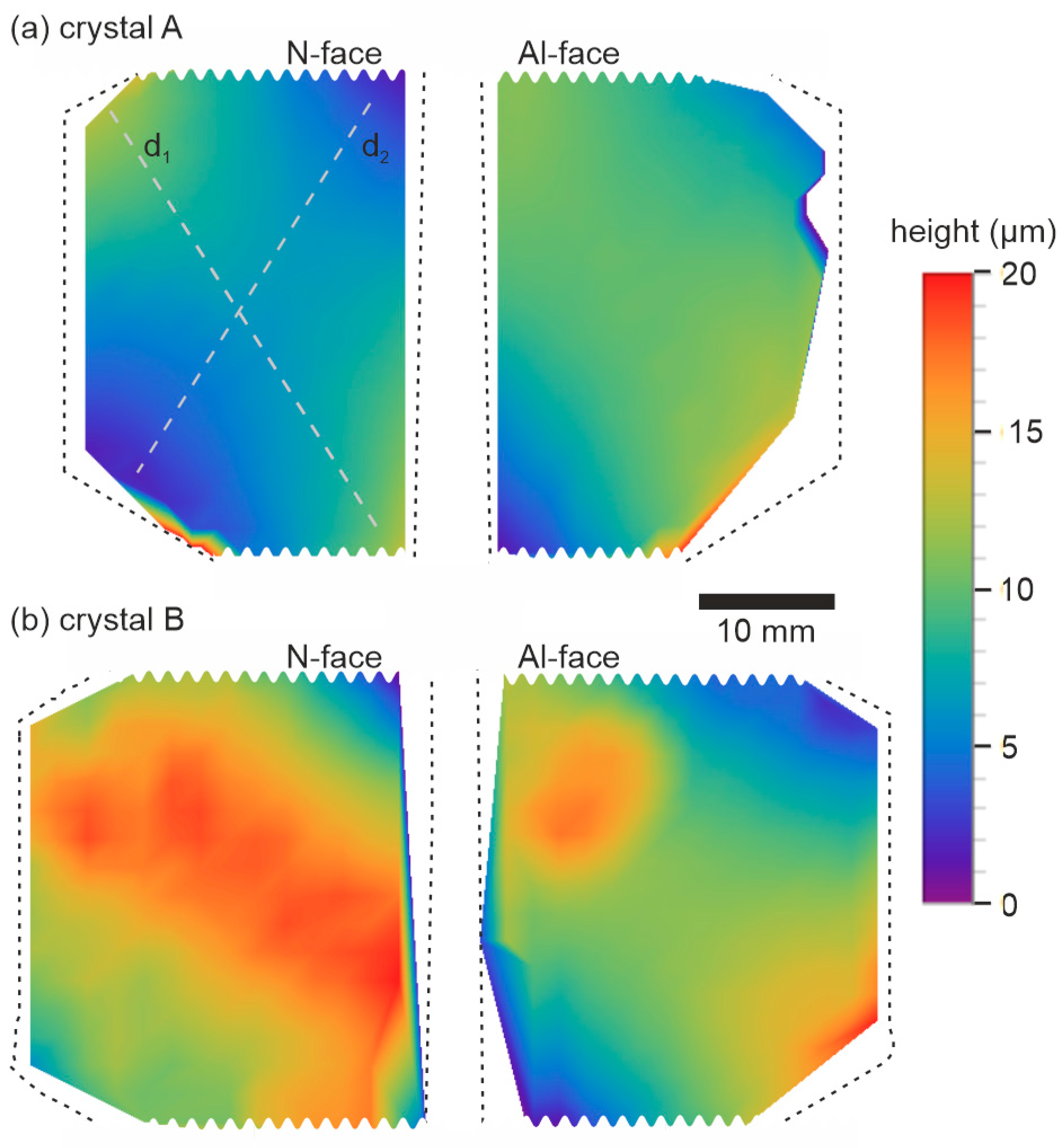
3.1. Crystal Habit, Lattice Curvature, and Facet Identification

Both crystals under investigation are uniform in thickness and have a trapezoid base form (c-plane) with a mean length of 40 mm and a trapeze height of 27 mm for crystal A and 30 mm for crystal B. The respective crystal borders are shown in Figure 5 by short-dashed lines for the Al-face, as well as the N-face, both aligned along the longer trapeze side. Please note that the fixation area collocated along the inclined part of the trapeze is masked by a wavelike perforation. We intentionally will neither show this part of the crystals nor discuss seed fixation throughout this work. The shape of both crystals is similar because of a similar seed geometry and comparable growth conditions. However, since the temperature gradient has been larger in crystal B (see Table 1), its dimension is larger than that of crystal A. This holds true especially for the thickness of crystal B since the growth velocity of the N-face is faster compared to the lateral growing faces [4,30].
Figure 5 shows the lattice shape (c-plane) near the N- and Al-face of both crystals in terms of height variation with respect to a reference plane chosen at a zero height. The crystal surface shape closely follows the lattice shape (no figure). The c-plane of both crystals is saddle-shaped with principal axes aligned along the diagonals d 1 and d 2 of the trapeze. Respective curvature radii r 1 and r 2 are noted in Table 4. Positive radii assign concave bending with respect to the reference plane, while negative values refer to convex bending. Note that the sign changes consistently for respective diagonals in the N-face and Al-face, indicating that the c-plane saddle-shape does not change qualitatively, as expected. However, three observations are remarkable: first, the absolute value of the radii of both diagonals are the same in crystal A and similar in crystal B within the error of curvature of radius of approximately 3 m, which indicates a high symmetry of the saddle-shape, especially in crystal A, as can be seen in Figure 5a. Second, the lattice shapes of both crystals are similar to each other, and third, the absolute curvature radius is lowest at the Al-face (~30 m) and becomes highest (~50 m) at the N-face for both crystals (see Table 4). The seed is in a floating configuration in the growth chamber, and growth takes place on both the Al- and N-face of the seed. However, growth speed of the N-face is significantly higher than that of the Al-face since material transport inside the growth chamber is tailored towards the N-face. In our case that means that the c-plane curvature of the crystal’s Al-face basically reflects the c-plane curvature of the seed. Since the seeds of both crystals have been adjacent wafers from a common crystal with the same seed conditioning, they are expected to have similar c-plane shapes leading to the same absolute values of the curvature of radii in crystals A and B at the Al-face, as observed. The lowering of the curvature towards the N-face can be understood in terms of the incorporation of basal plane dislocations with an appropriate Burgers vector during growth in order to follow the flat temperature field of the setup. This is commonly observed in the PVT growth of 4H-SiC [31,32], and we assume that we have a similar situation here. In the forthcoming chapter, we will show that, especially at the border of the crystal, a significant content of basal plane dislocation clusters can be identified, which may lead to smoothing the curvature of the crystals towards the N-face.
The flatness of all boundaries of the crystals and the sharpness of the edges indicates that any of these are true facets defined by highly symmetric crystallographic planes. This is indicated by their geometry, crystallographic orientation, and step flow structure (no figure). Our facet indexation is presented in X-ray topography images in Figure 6a,b. Topographs in back-reflection geometry of all crystal surfaces have been taken with the respective reflections corresponding to the facet orientation, as indicated in the figure. The dominant facets are the polar facets of the c-plane, namely 0001 (Al-face) and 000 1 ¯ (N-face). As we have seen in Figure 5, lattice shape measurements show the overall flatness of these basal plane facets. The crystal is laterally terminated completely by fully developed nonpolar m-plane facets 10 1 ¯ 0 , which could be verified through X-ray topography, proving their identity. Adjacent m-facets form a sharp edge with a 120° angle, as expected. In particular, no trace of a-facets 11 2 ¯ 0 can be observed. This indicates that faster growing a-facets disappeared in favor of the slower-growing adjacent m-facets during growth [4,30]. Deviation from the faceting naturally occurs only close to the Al-face for our crystals. The development of the growth front until the facets are completely formed will be discussed in the three-dimensional section topography in Section 3.4.

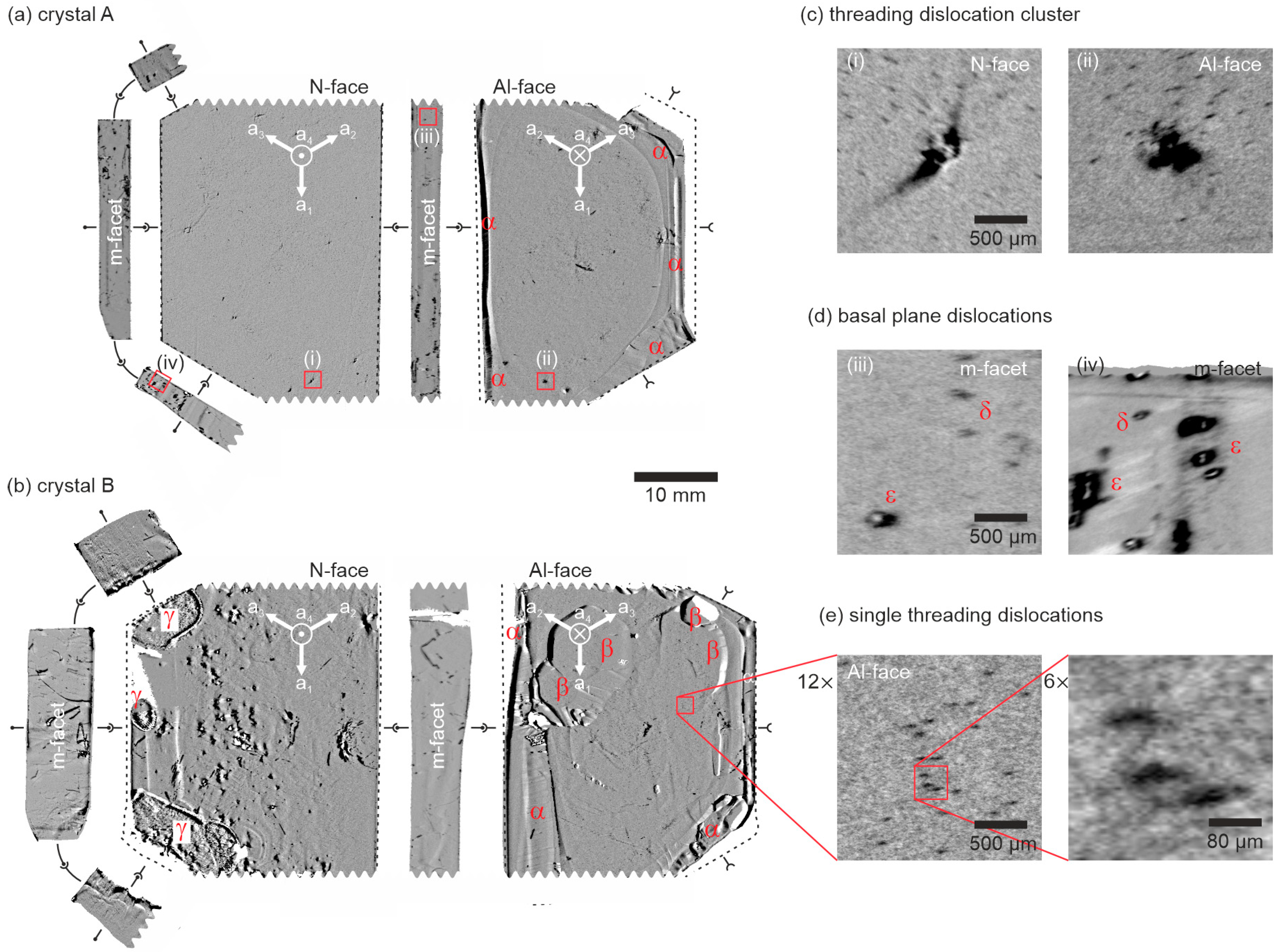
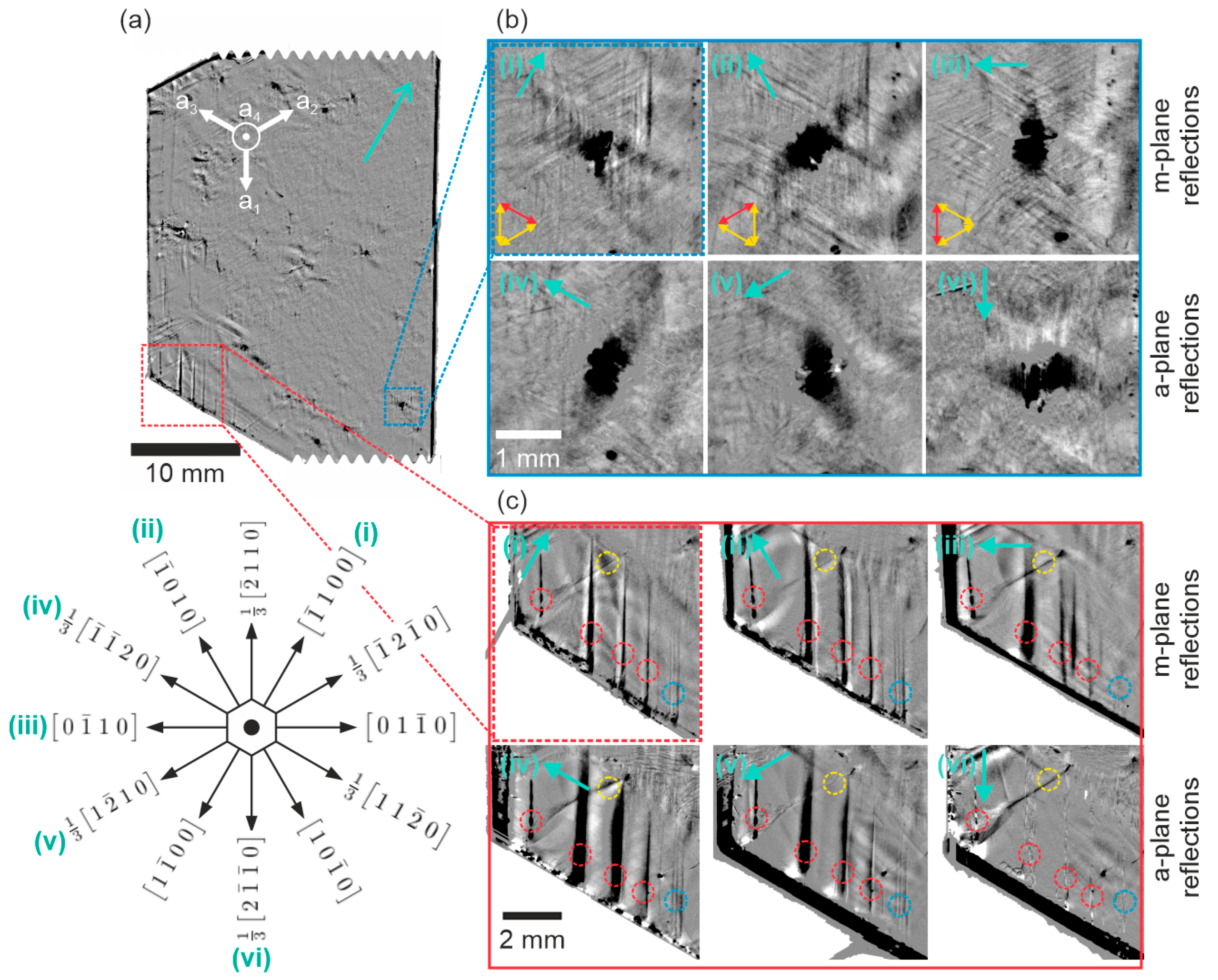
3.2. X-Ray Topography in Back-Reflection Geometry of the Crystal Surface

In Figure 6a,b, the full surface net of all formed facets from both crystals are shown in back-reflection topography. The symmetric reflections used are recorded in Table 3. They have been chosen to have the highest intensity and to be accessible in our instrument. If a surface is sufficiently flat in a geometrical sense, its topography does not play any role in the interpretation of contrasts in the X-ray topographs. This is especially the case for native facets of our crystals. One exception is the rim of the Al-face, where unsmooth or inclined parts are observed (see features α in Figure 6). In addition, crystal B shows hexagonal V-pits on the Al-face (see features β in Figure 6) and unsmooth surface parts (see features γ in Figure 6) giving rise to absorption contrast. However, there are no preparation damages as it may occur for wafers since the surface is as-grown. The lattice curvature for both crystals could be accounted for using the lattice curvature correction method such that the interpretation of the topography contrast is determined by crystal defects, except for the mentioned parts of the Al-face.
The advantage of topography in reflection geometry, in contrast to topography in transmission geometry, is that there is no restriction to the thickness of the crystal. The penetration depth is typically of the order of tens of micrometers (see Table 1), such that only information close to the crystal’s surface is obtained. For example, it has been shown in [33] that the observable depth of dislocations in 4H-SiC is ¾ of the absorption depth. Since AlN is isoelectronic to SiC, we expect similar behavior for AlN. The excitation volume is small, and an interpretation of contrasts is easier compared to transmission topography where overlap of the defect-related contrasts takes place due to the integral nature of the measurement. Two types of defects are dominating the c-plane topographs (see Figure 6c,e). The smallest features are dark spots of an elliptic shape with the semi-minor axis, typically 20 µm in length and with an eccentricity of 0.9 (see Figure 6e). The major axis of the ellipses is pointing towards the scattering vector since the threading dislocation is viewed approximately under the Bragg angle. They can be attributed to threading dislocations with screw components. Note that threading edge dislocation cannot be detected based on a symmetric reflection since they are forbidden by the g · b —selection rule [34]. Although in principle asymmetric reflections would allow one to detect the threading edge dislocations, their intensity is too low to make an evaluation feasible. Therefore, we restrict the bulk surface inspection to an evaluation of topographs measured under symmetric reflection geometry and assign detected dark spots as threading dislocations (TDs). Apart from the individually resolvable threading dislocations, we observe much larger defects of an undefined shape, as can be seen in Figure 6c. They are particularly strong in contrast and can be considered a clustering of dislocation, typically arranged in close chains [17], assigned as defect clusters in this work. They have significantly higher intensity compared to single dislocations since the clustered dislocations form an accumulated stress field. For the m-facets, we can draw similar conclusions as for the c-plane topographs. As can be seen in Figure 6d, small dark spots (feature δ) can be identified as single basal dislocations with screw components, whereas strong basal dislocation clusters are also present (feature ε). It is the latter that may play a central role in stress relaxation during crystal formation.
With common methods of image processing, it is straight forward to determine the threading dislocation density, as well as the cluster density, automatically. The results are shown in Figure 7 for the N- and Al-face of crystal A, as well as for the N-face of its seed. The mean dislocation density is 480 ± 30 cm−2 for crystal A and B for both faces. Apart from the total defect density, we can observe the spatial defect distribution and get an idea about the defect propagation throughout the bulk of the crystal. Very clearly, we can see that the defect distribution pattern is globally preserved from the seed to both crystal surfaces. Even in the case of the N-face of the crystal, where the observed threading dislocations have propagated a relatively long distance through the volume compared to the place of the seed interface, the pattern has not changed significantly. Some additional observations are remarkable. In general, the defect pattern is dominated by the cluster defects with most of them keeping their lateral position and even though some of them are being dissolved.
Individual threading dislocations cannot be traced from the seed to neither the N-face nor the Al-face of the crystal. This indicates that they undergo strong interactions during growth leading to bending and/or transformations into basal-plane dislocations or they do not propagate strictly along the c-axis. However, in contrast to the section topo-graphy, surface inspection of the crystal alone cannot reveal any details of how threading dislocation networks evolve, for instance, whether dislocation bending or transformation dominates.
After this general description, we show that the defect density distribution charts can be used to qualify the new laterally grown material, which is of specific interest in terms of diameter expansion. Comparing, in Figure 7, the outline of the seed (a) with that of the bulk crystal (b,c), we can identify the laterally grown part in the magnified image (see Figure 7e) marked by the red dashed line. Essentially, only the part that deviates from the m-facet shows significant lateral growth of new material beyond the outer seed rim, which is driven by a-facetted growth. It is intriguing and of high relevance to note that almost no threading dislocations with a screw component were generated in this part (blue intensity region in Figure 7e beyond the seed boundary). Together with the fact that the pattern of dislocation distribution of the seed (Figure 7a) is similar to the N-face of the crystal (Figure 7b), this indicates that the origin of the TDs in the region over the seed is mainly induced by the dislocations in the seed. However, we cannot deduce the threading edge dislocation and the basal plane dislocation content from these topographs. Therefore, a conclusive defect analysis of this newly grown part cannot be performed through surface inspection alone. Integrated bulk and/or section topography need to complete the picture through an identification of basal plane defects in this area, as shown in the next sections.

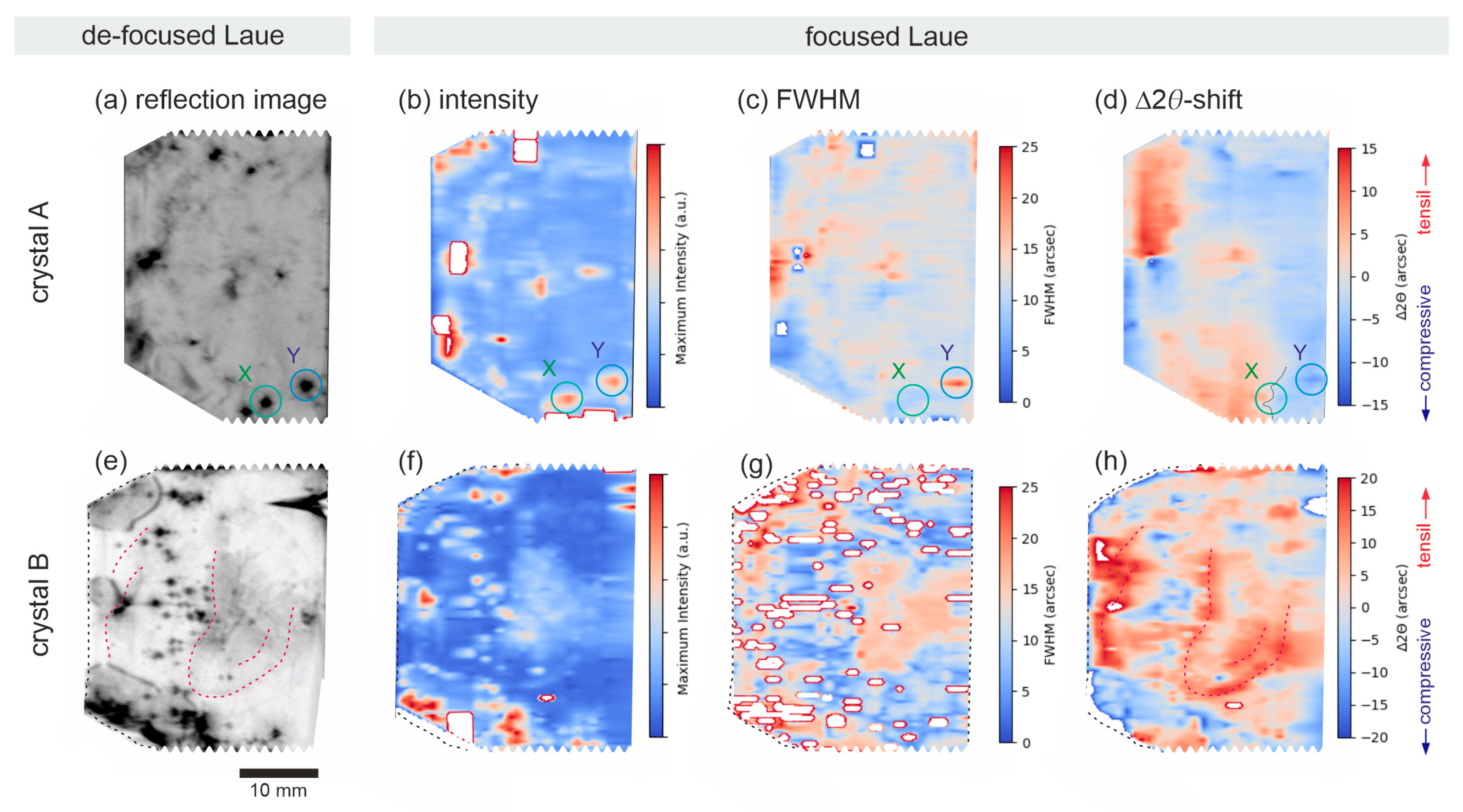
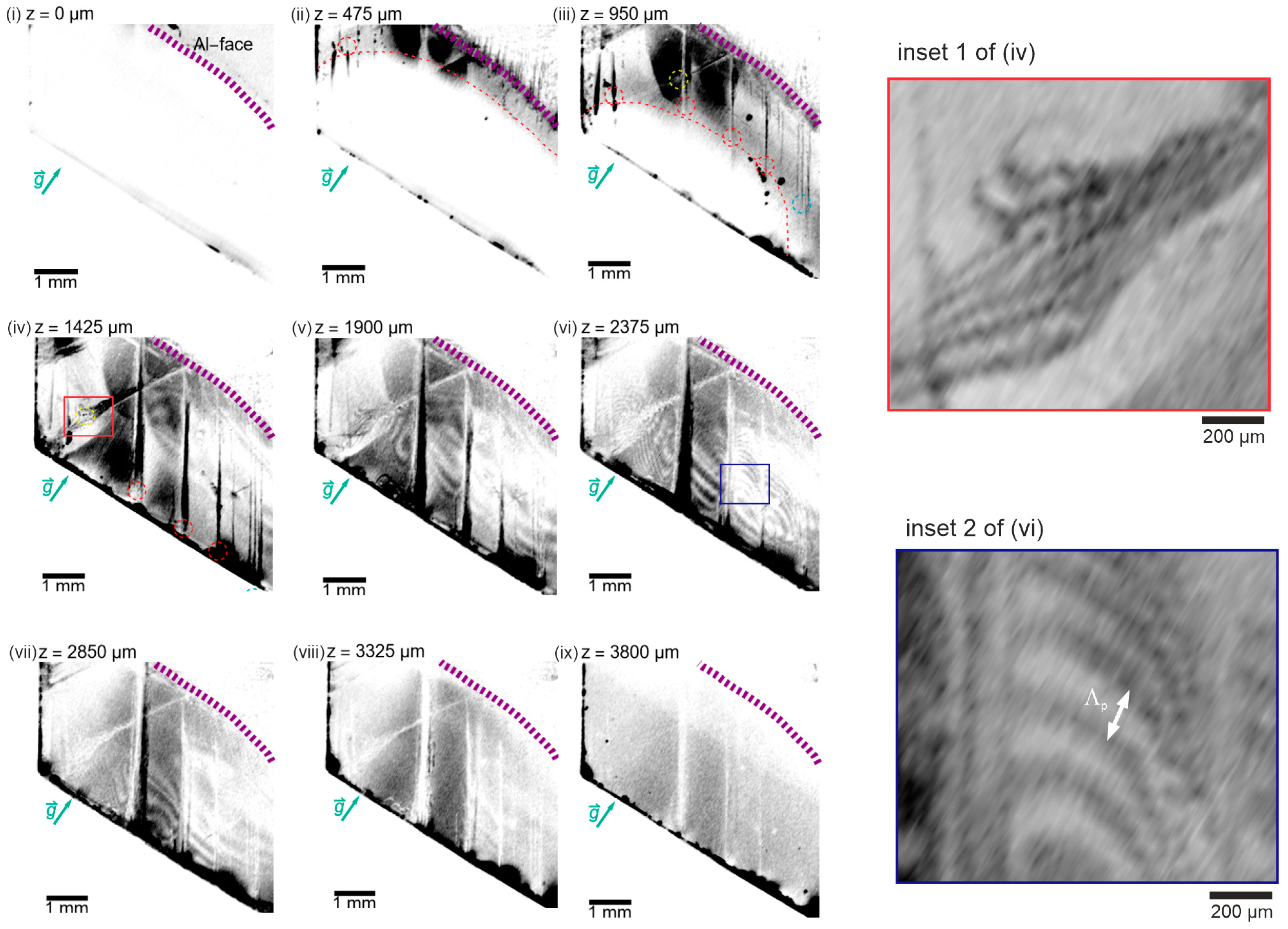
3.3. Integrated Bulk Characterization

Contrary to the topography in back-reflection mode, in Lang transmission topography, the X-rays must be able to penetrate the crystal. Therefore, high-energy X-rays are mandatory. Even more, for materials like AlN and a Cu-anode as an X-ray source, a wafer thickness of 500 µm is already too thick for transmission measurements (see Table 1 for penetration depths) with an acceptable signal-to-noise ratio (SNR). Silver and tungsten anodes are suitable candidates for penetrating thick crystals. However, it was not possible to measure crystal B with the Ag anode, whereas with the Laue setup with the W anode, both crystals could be measured with acceptable SNR and topograph quality. Figure 8a shows the topograph of crystal A measured in Lang transmission using the Ag: 10 1 ¯ 0 reflection, and Figure 9a shows the same crystal with de-focused Laue transmission with a W: 10 1 ¯ 0 reflection. Both topographs show a coincident distribution of the cluster defects and coincidence in their dislocation pattern. However, in the Lang transmission topographs, the SNR is much better, attributed to the long integration time of 24 h, whereas the integration time in the Laue setup was only 1 h.
According to the g·b criteria [34,35], it is well established that three distinct g vectors are sufficient to determine the Burgers vector unambiguously: one reflection where the dislocation is visible and two reflections where the dislocation is extinguished. The intersection of the latter two reflection planes determines the Burgers vector up to its sign. However, some observations make this process difficult. First, the g·b criteria itself is an idealized rule, which may not lead to a complete extinction of the reflection rather than a (significant) diminution of the contrast. The weak contrast visible under the condition of g·b = 0 is expected to be due to the behavior of the strain field expanded on the sample surface (surface relaxation effect) [36,37]. Second, not all reflections of interest are accessible in an XRT system, so conclusions must be drawn from a non-ideal set of reflections. Third, in the case of a bundle of dislocations (clusters) where individual dislocations may have different Burgers vectors, the g·b criteria are not applicable. Last, the line vector is not always along crystallographic directions and may not be straight within the excitation volume of the topograph, leading to unpredictable intensity variations. Although the above-mentioned difficulties are present in this work, we show that in some cases, we are able to determine the Burgers vector or at least establish restrictions to its possible directions.
We apply the g·b criteria to most common dislocation types and directions (see Figure 10). Typical Burgers vectors are the 0001 (c-type), 01 1 ¯ 0 (m-type), and 1 3 1 ¯ 2 1 ¯ 0 (a-type) direction family. Although the c + a type (mixed type) may be present, no extinction can be achieved for any reflections, so they are not considered explicitly in the table. The basal plane dislocations along the a-planes and threading dislocations are considered. The measured reflections are the 01 1 ¯ 0 family (m-planes) and the 1 3 1 ¯ 2 1 ¯ 0 family (a-planes) shown in the upper three and lower three pictograms in the table, respectively. The corresponding six topographs are shown in Figure 8b for a typical threading dislocation cluster surrounded by basal plane dislocations and in Figure 8c for bundles of basal plane dislocations ending at the m-facet, marked by a blue and red rectangle in Figure 8a, respectively.
The threading dislocation cluster in the center of the topographs in Figure 8b is always seen for all six reflections very clearly. The shape of the cluster appears like a snowflake elongated in the measurement direction (perpendicular to the g-vector), which is caused by the projection of the camera onto the sample plane. For neither reflection plane, we can identify a diminution of the contrast intensity. According to Figure 10, this is consistent with edge dislocations. As we know that such clusters consist of bundles of threading dislocations [17], we can conclude that the majority of them has Burgers vectors with an edge component. Around the cluster, we see a pronounced set of basal plane dislocations collocated along the m-planes in a David star like pattern. From Figure 8b (i) to (iii), basal planes are not visible if the lattice vector is perpendicular to the basal plane under consideration (red double arrow), while the other basal planes are present (yellow double arrow). Note that in the a-plane topographs of Figure 8b (iv) to (vi), all basal planes are visible, although the contrast is lower, and the identification of individual basal planes is difficult. By looking at Figure 10 these basal plane dislocations can be identified as screw-type, i.e., they have a Burgers vector parallel the dislocation line.
In the topographs of Figure 8c, we draw our attention to the dislocation bundles, which go straight along the 1 3 2 1 ¯ 1 ¯ 0 direction family, marked with red, blue, and yellow circles. Note that the dislocation bundles marked by the red circle are clearly seen in all topopgrahs1, indicating that we have a similar situation as for the threading dislocation cluster in Figure 8c, i.e., the Burgers vectors cannot be identified. The situation for the dislocations marked by the blue and yellow circles is different. First, we see that the dislocation lines themselves are significantly thinner indicating that we have individual dislocations. For the blue circle in Figure 8b (iii), the dislocations are (almost) invisible, while they are seen in all other topographs (please note that the dislocations marked by the red and blue circles in Figure 8c (vi) are barely seen in the post-processed image but are clearly seen in the original topograph (no figure). The same applies to the dislocation marked by the yellow circle in Figure 8c (v). We keep all topographs post-processed showing optimal contrast to the eye.). According to Figure 10, we expect a Burgers vector of 1 3 2 1 ¯ 1 ¯ 0 . Together with the line vector in the same direction, we conclude that these dislocations are of the screw type. We have the corresponding situation for the dislocation marked by the yellow circle: it is (almost) not present in topograph (ii) but visible in all others, concluding a Burgers vector of 1 3 1 ¯ 2 1 ¯ 0 with a line vector in the same direction (screw dislocation).
Comparing the 10 1 ¯ 0 reflection topographs (m-plane) in the de-focused Laue transmission mode of crystal A (Figure 9a) with Lang transmission (Figure 8b, iii), we see, in principle, the same defect structure. Differences arise merely from the camera resolution and exposure time. However, the focused Laue transmission mode gives rise to additional information, which is not present in a reflection topograph. The fitting procedure of Pseudo-Voigtian gives additional parameters, which have physical significance and can be presented as mappings [38]. We present the mappings for the intensity (Figure 9b,f), full width at half maximum, FWHM (Figure 9c,g), and peak shift in units of 2 θ (Figure 9d,h). All mappings show essentially the same defect structure as can be seen when comparing them with the respective de-focused Laue or Lang transmission topographs. Especially, we expect this for the intensity mapping which, can be considered a measure of control for the acceptance of the global fitting results (apart from the fitting errors). Notable differences arise in FWHM mappings and the 2 θ -shifts. Note that the 2 θ -mapping reflects the local misorientation of the lattice; thus, it is a measure of local strain induced by the stress field of the dislocations.
The mean value of the FWHM of crystal A and B is 10.6 and 11.3 arcsec, respectively. Since only thickness broadening of the FWHM has been considered and not the response function for the setup, these values are understood as an upper limit and show the overall good quality of both crystals in the cluster-free region. This is consistent with the fact that both crystals have the same low mean threading dislocation density of 480 ± 30 cm−2, as shown in Section 3.2.
The green and blue circle mark two clusters X and Y, respectively (Figure 9a,d). The latter has been investigated intensively before and is shown in Figure 8b, whereas the other cluster is not shown here in detail but exhibits the same interpretation when looking at the Lang transmission topography only. However, we clearly see that in the FWHM mapping and in the 2 θ -shift mapping, cluster Y is visible, whereas cluster X is absent, giving evidence for a difference. A possible explanation can be derived from the 2 θ -mapping where we see that through the position of cluster X, the neutral fiber (dotted line, absence of internal pressure) running through it, separating two parts of tensile and compressive stress, whereas cluster Y is located completely in the region of compressive stress. This may lead to the conclusion that we do not have a stress-induced broadening of the FWHM for cluster X, but that it is present in cluster Y.
In crystal B, we observe a larger density of clusters than in crystal A as can be seen in Figure 9a,e, especially at the lower left m-facet. It is remarkable that in the region of high tensil stress, marked by a red dashed line in Figure 9h, the corresponding region in Figure 9e shows region with a low number of clusters or even partially a cluster-free region.

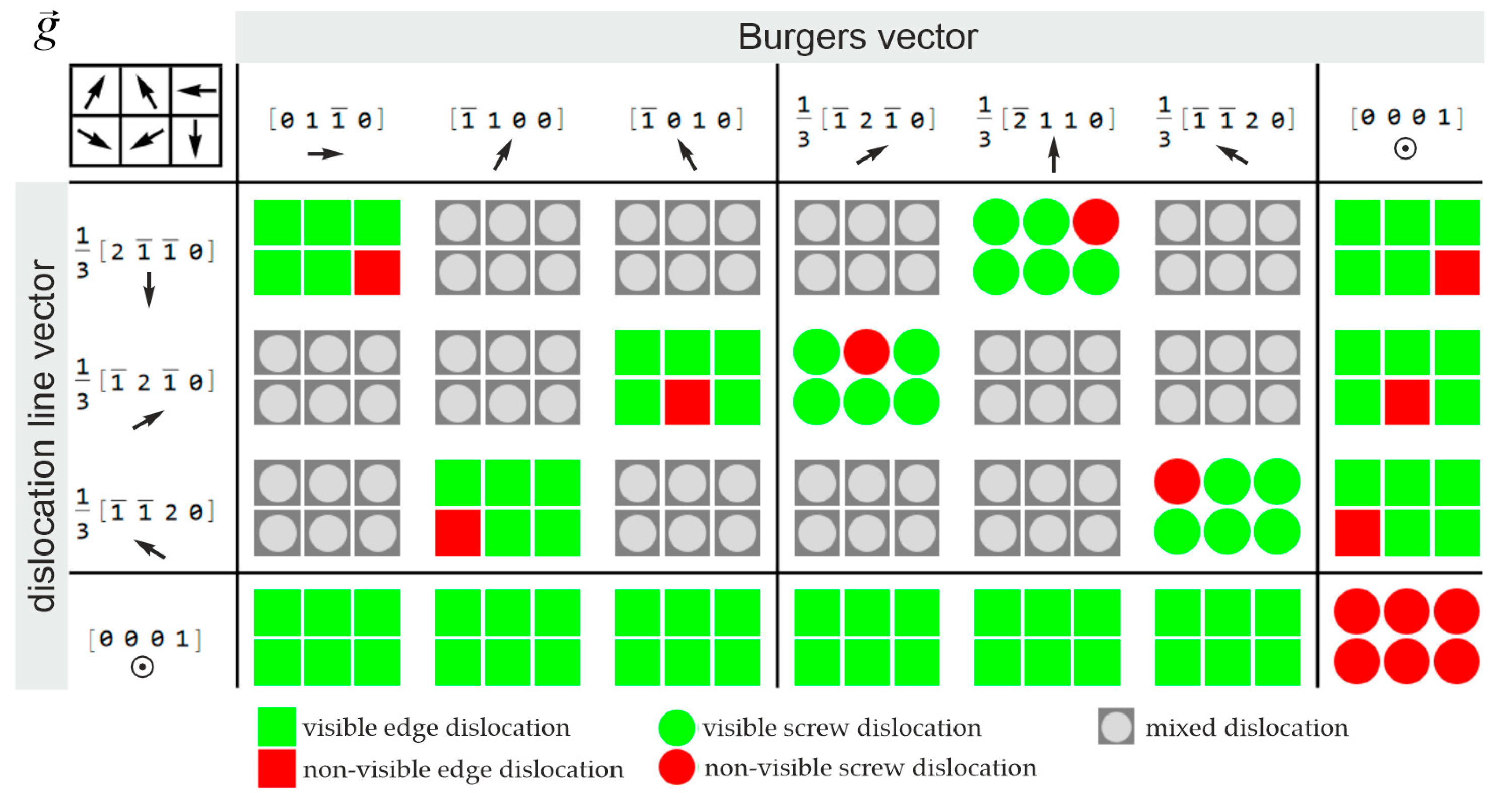
3.4. Three-Dimensional Dislocation Modeling—Revealing the Borrmann Effect

In principle, the same reflections and anode materials as for the integrated bulk inspection can be used for section topography. However, it is recommended to choose reflections with large Bragg angles to enhance pixel resolution due to the projection angle onto a section (see Figure 4c). Section topographs with a tungsten anode have less resolution along the c-axis, and we restrict the section topography on crystal A to the Ag anode in this work. A resolution in the c-axis of approximately 25 µm per pixel could be achieved.
The red rectangular part marked in Figure 8a was measured through section topography as described in Section 2.3.4. The measurement covers 200 section topographs starting from the m-facet (position at x = 0 ) towards the center of crystal A (position at x = 3 mm ) in steps of 50 µm. The effective size of the excitation volume of one section slice was 26 µm such that basal plane dislocations appear almost as smooth lines. Re-slicing the stack of section topographs in the z-direction results in an image sequence starting from the Al-face (backside of the seed) towards the N-face. Nine selected images out of this re-sliced stack are shown in Figure 11. In the following, we derive detailed information for the orientation of the basal plane dislocation cluster, also showing that they consist of bundles of individual dislocations. Finally, we will discuss the evolution of the lateral growth front.
Basal dislocation clusters marked in Figure 8c are shown correspondingly in the nine topographs of Figure 11. The growth front is indicated by a dashed red line. Note that in (i), corresponding to the Al-face at z = 0 , the growth front shows essentially the seed border (purple dashed line). Towards the N-face, the growth front is driven by fast growth in the a-direction until m-facets are built at z = 1425 µm (iv). In continuation of growth, only small development of the m-facets takes place. Comparing the crystal evolution in the a-direction to that in the m-direction, a growth velocity ratio v a / v m = 3 can be derived, commonly observed in our AlN bulk growth.
It is evident that, already at the seed border, the basal plane dislocation clusters, marked red and yellow in Figure 11 (iii) and (iv), are generated and follow the growth front along the 1 3 2 1 ¯ 1 ¯ 0 directions. The line vector of these dislocations is not exactly within the basal plane, leading to a small mixed character of the dislocation. The dislocation bundle marked by a yellow circle dissolves in the range from z = 1425 µm (iv) to z = 1900 µm (v) into single dislocations, which can be seen in the inset. Moreover, for the red marked bundles dissolving of the dislocations close to the facets can be observed justifying the classification of them as dislocation bundles or clusters. The dislocations marked by blue circle in Figure 8c and Figure 10 behave differently. They also start at the seed border but are maintained in the basal plane. This can be nicely verified by re-slicing the stack along the y-direction (see Supplementary Material, Videos S1 and S2).
The dynamical diffraction contrast (Borrmann effect [10]) shows up clearly as characteristic intensity fringes in the range from z = 1425 µm to z = 3325 µm below the basal plane clusters (Figure 11 iv to viii). The mean separation of the fringes is about 150 µm, which is in close agreement to 133 µm, which is the estimated length of the Pendellösung  Λ p given by the following formula:
Λ p = π cos θ B Λ = π 2 V cos θ B λ r e F
In this equation, Λ is the extinction length, V the volume of the unit cell, r e the classical electron radius, F the structure factor, and θ B the Bragg angle of the m-plane reflection at the wavelength of the characteristic line λ of silver. To the best of our knowledge, it is the first time that the Borrmann effect has been demonstrated for PVT-grown AlN, and this is the featured novelty of this publication. It is known that dynamical effects, like fringes in the intensity contrast, cannot be expected for material with even moderate dislocation densities. Therefore, we can conclude that for the topographic part where the fringes are observed, the crystal is of extraordinary high structural quality. The fringes caused by the Borrmann effect are expected in the absence of threading screw dislocations (Figure 7e), low curvature (Figure 5a), and low FWHM, measured via focused Laue diffraction (Figure 9c) in the respective area. Note that the basal plane clusters are all identified as located at the surface so they do not interfere the defect-free part of the crystal where the fringes are visible.

4. Conclusions: Assessment of Methods

In this work, we have presented comprehensive measurement results of two PVT-grown AlN bulk crystals via X-ray topography in back-reflection geometry (surface inspection), Lang- and Laue transmission topography (bulk inspection), and three-dimensional section topography. It is obvious that all three methods have their advantages and disadvantages depending on the applications and scientific or engineering requirements. A main objective of this work is the assessment of these methods and clarification of the best area of application. For this, we summarize them in Table 5. The table intentionally does not show absolute values because they are material- and instrument-dependent. However, it serves as a guideline and helps to choose the appropriate method to obtain the best results.
The surface inspection method has the advantage that it is relatively fast and is, per definition, not thickness-dependent. However, depending on the penetration depth of the anode material used, only the dislocation content close to the surface can be identified. Some additional information from the inside of the bulk can be gained indirectly from lateral facets assuming that the dislocation variation inside the bulk is not too large. Typically, threading dislocations are clearly identified as dark spots, and even their Burgers vector can be analyzed by using appropriate asymmetric reflections (not performed in this work). Mappings for dislocation densities give characteristic distribution patterns, which may be correlated with growth conditions.
On the other hand, the bulk inspection method, like the Laue and Lang-transmission method, can penetrate the whole crystal, at least if the energy of the X-ray is high enough and the crystal is not too thick. This leads to integrated information of the dislocation content inside the crystal. Especially, if there is a very low or no dislocation content, the interpretation of the topograph is straight forward. However, for even moderate dislocation content, where massive overlap of dislocations in the measurement direction occurs, tracing individual dislocations is impossible. Contrary to the surface inspection method, where only for asymmetric reflections, the surface near the basal plane dislocation can be detected, integrated transmission topography can reveal basal plane dislocations deep inside the bulk. In our case, the surface inspection suggests that the newly grown part of our crystal is free of dislocations since no threading screw dislocations could be detected. However, the bulk inspection reveals the strong presence of basal plane dislocation clusters along crystallographic directions, especially close to adjacent m-facets. A drawback of bulk inspection is the relatively long integration time needed to have topographs that are sufficient for analysis.
The three-dimensional section topography is essentially a bulk inspection tool and thus suffers the same disadvantages. The measurement times are even longer, because in addition to the penetration of thick crystals, many slices must be measured. Therefore, often, a compromise must be found, like the restriction of the measured region or reduction of the resolution. However, since the result is essentially a three-dimensional topograph of the bulk crystal, it is justified to classify it as its own category in Table 5. Apart from the same advantages as for the bulk inspection, we can gain a three-dimensional model of the crystal. For example, we can determine, unambiguously, the full trajectory of single dislocations or dislocation bundles. Another advantage is that dynamical effects within the bulk can be made visible, showing the high quality of crystals in such respective parts. This is not possible with the other methods since they either do not detect such regions (in the case of surface inspection) or are blurred by defective regions in the integrated bulk inspection. For example, in case of crystal A, we could clearly show that the lateral expanded part is of extraordinary high quality, which is an essential feedback for lateral diameter expansion in crystal growth. Regarding the novelty, it should be emphasized that the Borrmann effect has been demonstrated in PVT-grown bulk AlN.
Finally, it should be noted that the methodologies presented here are demonstrated explicitly for the example of AlN. However, other materials with comparable defect densities, such as SiC, can be investigated in the same way.

Supplementary Materials

The following supporting information can be downloaded at: https://www.mdpi.com/article/10.3390/cryst15050449/s1, Video S1: Section topography of crystal A: the central panel shows a video sequence of 156 topographs from z = 0 µm (Al-face) to z = 3800 µm (N-face). Topographs that are taken in Figure 10 are marked (i) to (ix). Clusters of interest are marked by circles. Two profile sections are shown in the upper and lower panels and are marked in the central panel by respective colored dashed lines; Video S2: Section topography of crystal A: the upper panel shows the topograph section at z = 1500 µm (center of the bulk). The lower panel shows the video sequence of section topographs from y = 0 µm to y = 4863 µm. The current section in the video is indicated in the upper panel by a dashed line. Clusters of interest are marked by dashed lines and circles. Colors correspond to those in Video S1.

Author Contributions

Writing—Original draft preparation, R.W.; conceptualization, R.W. and S.B.; review and editing, S.M. and S.B.; crystal growth, G.L., A.L. and B.E.; High-energy Laue setup, M.W. and R.W.; data evaluation, R.W., L.S. and S.B.; Project administration and funding acquisition, S.M., E.M. and S.B. All authors have read and agreed to the published version of the manuscript.

Funding

This research was funded by the German Federal Ministry for Education and Research, grant numbers 16ES1110, 16ES1111, and 16KISK134.

Data Availability Statement

The original contributions presented in the study are included in the article/Supplementary Material; further inquiries can be directed to the corresponding author.

Conflicts of Interest

The authors declare no conflicts of interest.

Appendix A. Measurement Procedure for X-Ray Topography

The measurement procedure for the back-reflection and transmission measurements using the XRTmicron follows a three-step procedure:
First Step. After the sample is placed onto a Kapton® foil [28] sample holder and the goniometer is set to the required reflection condition, an alignment procedure at the center of the sample is performed with a scintillator detector. The goniometer angles are aligned to match the desired diffraction conditions. In the case of Lang transmission (m- or a-plane), a 360-degree sample rotation scan is performed, in order to determine which of the six equivalent m-planes is already best aligned. For symmetric reflection in back-scattering geometry, the respective sample surface is typically manually aligned such that a rocking curve measurement can be performed directly. The source and detector angles are oriented to the maximum of the resulting Kα1 line. Successive sample rotation is performed to find the best sample orientation. This procedure is repeated iteratively—typically about three to five times—until the optimal rocking and sample rotation angle is found.
Second Step. Due to the sample’s lattice curvature, the sample is not under optimal diffraction conditions at all of its positions. Therefore, rocking curves are recorded at selected positions of the sample, while the sample rotation has been kept fixed. In our case, one row with steps of 2 mm was sufficient. The result is used for lattice curvature correction while performing topography mapping.
Third step. The time delay integration method enables the imaging of the X-ray diffraction intensity of the sample “on the fly”, i.e., the stage continuously moves in the x-direction. If the extent of the sample in the y-direction is larger than the camera’s field of view, the y-axis is adjusted accordingly, and an additional band is measured. All bands are finally stitched to the full topograph. Intensity background gradients due to local orientation contrasts that could not be corrected for by curvature correction in step 2 were eliminated using standard image-processing methods of the raw topographs.

References

  1. Doolittle, W.A.; Matthews, C.M.; Ahmad, H.; Motoki, K.; Lee, S.; Ghosh, A.; Marshall, E.N.; Tang, A.L.; Manocha, P.; Yoder, P.D. Prospectives for AlN electronics and optoelectronics and the important role of alternative synthesis. Appl. Phys. Lett. 2023, 123, 070501. [Google Scholar] [CrossRef]
  2. Glenn Zorpette. The New, New Transistor. Available online: https://spectrum.ieee.org/aluminum-nitride (accessed on 8 May 2025).
  3. Semiconductor Today. HexaTech Investment Accelerates 100 mm AlN Substrate Program. Available online: https://www.semiconductor-today.com/news_items/2022/oct/hexatech-061022.shtml (accessed on 8 May 2025).
  4. Bondokov, R.T.; Hogan, K.; Norbury, G.Q.; Mark, J.; Branagan, S.P.; Ishigami, N.; Grandusky, J.; Chen, J. (Invited) Development of 3-inch AlN Single Crystal Substrates. ECS Trans. 2022, 109, 13–19. [Google Scholar] [CrossRef]
  5. Chen, W.-H.; Qin, Z.-Y.; Tian, X.-Y.; Zhong, X.-H.; Sun, Z.-H.; Li, B.-K.; Zheng, R.-S.; Guo, Y.; Wu, H.-L. The Physical Vapor Transport Method for Bulk AlN Crystal Growth. Molecules 2019, 24, 1562. [Google Scholar] [CrossRef]
  6. Dalmau, R.; Sitar, Z. AlN Bulk Crystal Growth by Physical Vapor Transport. In Springer Handbook of Crystal Growth; Dhanaraj, G., Byrappa, K., Prasad, V., Dudley, M., Eds.; Springer: Berlin/Heidelberg, Germany, 2010; pp. 821–843. ISBN 978-3-540-74182-4. [Google Scholar]
  7. Sumathi, R.R. Review—Status and Challenges in Hetero-epitaxial Growth Approach for Large Diameter AlN Single Crystalline Substrates. ECS J. Solid State Sci. Technol. 2021, 10, 35001. [Google Scholar] [CrossRef]
  8. Amano, H.; Collazo, R.; de Santi, C.; Einfeldt, S.; Funato, M.; Glaab, J.; Hagedorn, S.; Hirano, A.; Hirayama, H.; Ishii, R.; et al. The 2020 UV emitter roadmap. J. Phys. D Appl. Phys. 2020, 53, 503001. [Google Scholar] [CrossRef]
  9. Hartmann, C.; Kabukcuoglu, M.P.; Richter, C.; Klump, A.; Schulz, D.; Juda, U.; Bickermann, M.; Hänschke, D.; Schröder, T.; Straubinger, T. Efficient diameter enlargement of bulk AlN single crystals with high structural quality. Appl. Phys. Express 2023, 16, 75502. [Google Scholar] [CrossRef]
  10. Lider, V.V. X-Ray Diffraction Topography Methods (Review). Phys. Solid State 2021, 63, 189–214. [Google Scholar] [CrossRef]
  11. Danilewsky, A.N. X-Ray Topography—More than Nice Pictures. Cryst. Res. Technol. 2020, 55, 2000012. [Google Scholar] [CrossRef]
  12. Dalmau, R.; Britt, J.; Fang, H.Y.; Raghothamachar, B.; Dudley, M.; Schlesser, R. X-Ray Topography Characterization of Large Diameter AlN Single Crystal Substrates. MSF 2020, 1004, 63–68. [Google Scholar] [CrossRef]
  13. Yao, Y.; Sugawara, Y.; Ishikawa, Y.; Okada, N.; Tadatomo, K. Crystallinity Evaluation and Dislocation Observation for an Aluminum Nitride Single-Crystal Substrate on a Wafer Scale. J. Electron. Mater. 2020, 49, 5144–5153. [Google Scholar] [CrossRef]
  14. Yao, Y.; Tsusaka, Y.; Ishikawa, Y.; Sugawara, Y.; Fujita, Y.; Matsui, J.; Okada, N.; Tadatomo, K. Study of dislocations in AlN single-crystal using bright-field synchrotron x-ray topography under a multiple-beam diffraction condition. Appl. Phys. Lett. 2020, 117, 092102. [Google Scholar] [CrossRef]
  15. Zhou, T.; Raghothamachar, B.; Wu, F.; Dalmau, R.; Moody, B.; Craft, S.; Schlesser, R.; Dudley, M.; Sitar, Z. Characterization of Threading Dislocations in PVT-Grown AlN Substrates via x-Ray Topography and Ray Tracing Simulation. J. Electron. Mater. 2014, 43, 838–842. [Google Scholar] [CrossRef]
  16. Raghothamachar, B.; Dudley, M.; Rojo, J.C.; Morgan, K.; Schowalter, L.J. X-ray characterization of bulk AIN single crystals grown by the sublimation technique. J. Cryst. Growth 2003, 250, 244–250. [Google Scholar] [CrossRef]
  17. Wicht, T.; Müller, S.; Weingärtner, R.; Epelbaum, B.; Besendörfer, S.; Bläß, U.; Weisser, M.; Unruh, T.; Meissner, E. X-ray characterization of physical-vapor-transport-grown bulk AlN single crystals. J. Appl. Crystallogr. 2020, 53, 1080–1086. [Google Scholar] [CrossRef] [PubMed]
  18. Straubinger, T.; Hartmann, C.; Kabukcuoglu, M.P.; Albrecht, M.; Bickermann, M.; Klump, A.; Bode, S.; Hamann, E.; Haaga, S.; Hurst, M.; et al. Dislocation Climb in AlN Crystals Grown at Low-Temperature Gradients Revealed by 3D X-ray Diffraction Imaging. Cryst. Growth Des. 2023, 23, 1538–1546. [Google Scholar] [CrossRef]
  19. Soukhojak, A.; Stannard, T.; Manning, I.; Lee, C.; Chung, G.; Gave, M.; Sanchez, E. Measurement of Dislocation Density in SiC Wafers Using Production XRT. MSF 2022, 1062, 304–308. [Google Scholar] [CrossRef]
  20. Christian Kranert, Christian Reimann, Shintaro Kobayashi, Yoshinoro Ueji, Kenta Shimamoto, Kazuhiko Omote. Scrutinising SiC with X-ray topography. Compd. Semicond. 2023, 29, 18–23. [Google Scholar]
  21. Kirste, L.; Grabianska, K.; Kucharski, R.; Sochacki, T.; Lucznik, B.; Bockowski, M. Structural Analysis of Low Defect Ammonothermally Grown GaN Wafers by Borrmann Effect X-ray Topography. Materials 2021, 14, 5472. [Google Scholar] [CrossRef] [PubMed]
  22. Kranert, C.; Wimmer, P.; Drouin, A.; Reimann, C.; Friedrich, J. Comparative study of methods for counting of dislocations in 4H-SiC. Mater. Sci. Semicond. Process. 2024, 170, 107948. [Google Scholar] [CrossRef]
  23. Bergmann, C.; Will, J.; Gröschel, A.; Weisser, M.; Magerl, A. Radial oxygen precipitation of a 12” CZ silicon crystal studied in-situ with high energy X-ray diffraction. Phys. Status Solidi A 2014, 211, 2450–2454. [Google Scholar] [CrossRef]
  24. Stockmeier, M.; Magerl, A. A focusing Laue diffractometer for the investigation of bulk crystals. J. Appl. Crystallogr. 2008, 41, 754–760. [Google Scholar] [CrossRef]
  25. Shul’pina, I.L.; Suvorov, E.V.; Smirnova, I.A.; Argunova, T.S. Section Methods of X-Ray Diffraction Topography. Tech. Phys. 2023, 68, 778–798. [Google Scholar] [CrossRef]
  26. Bearden, J.A. X-Ray Wavelengths. Rev. Mod. Phys. 1967, 39, 78–124. [Google Scholar] [CrossRef]
  27. Hubbell, J.; Seltzer, S. Tables of X-Ray Mass Attenuation Coefficients and Mass Energy-Absorption Coefficients 1 keV to 20 MeV for Elements Z = 1 to 92 and 48 Additional Substances of Dosimetric Interest. Available online: http://physics.nist.gov/PhysRefData/XrayMassCoef/cover.html (accessed on 8 May 2025).
  28. Wikipedia. Kapton. Available online: https://en.wikipedia.org/wiki/Kapton (accessed on 8 May 2025).
  29. Nilsson, D.; Janzén, E.; Kakanakova-Georgieva, A. Lattice parameters of AlN bulk, homoepitaxial and heteroepitaxial material. J. Phys. D Appl. Phys. 2016, 49, 175108. [Google Scholar] [CrossRef]
  30. Bickermann, M.; Epelbaum, B.M.; Filip, O.; Tautz, B.; Heimann, P.; Winnacker, A. Faceting in AlN bulk crystal growth and its impact on optical properties of the crystals. Phys. Status Solidi C 2012, 9, 449–452. [Google Scholar] [CrossRef]
  31. Cui, Y.; Hu, X.; Xie, X.; Wang, R.; Xu, X. Spatial variation of lattice plane bending of 4H-SiC substrates. CrystEngComm 2017, 19, 3844–3849. [Google Scholar] [CrossRef]
  32. Yang, X.; Yu, J.; Chen, X.; Peng, Y.; Hu, X.; Xu, X.; Yang, X.; Song, Y.; Wang, R. Basal plane bending of 4H-SiC single crystals grown by sublimation method with different seed attachment methods. CrystEngComm 2018, 20, 6957–6962. [Google Scholar] [CrossRef]
  33. Ishiji, K.; Kawado, S.; Hirai, Y.; Nagamachi, S. Determination of observable depth of dislocations in 4H-SiC by X-ray topography in back reflection. Jpn. J. Appl. Phys. 2017, 56, 106601. [Google Scholar] [CrossRef]
  34. Bowen, D.K.; Tanner, B.K. High Resolution X-Ray Diffractometry and Topography; Taylor & Francis: London, UK, 1998; ISBN 0-8506-6758-5. [Google Scholar]
  35. Authier, A. Dynamical Theory of X-Ray Diffraction; Oxford University Press: Oxford, UK, 2001; ISBN 9780198559603. [Google Scholar]
  36. Fujie, F.; Peng, H.; Ailihumaer, T.; Raghothamachar, B.; Dudley, M.; Harada, S.; Tagawa, M.; Ujihara, T. Synchrotron X-ray topographic image contrast variation of screw-type basal plane dislocations located at different depths below the crystal surface in 4H-SiC. Acta Mater. 2021, 208, 116746. [Google Scholar] [CrossRef]
  37. Ailihumaer, T.; Peng, H.; Fujie, F.; Raghothamachar, B.; Dudley, M.; Harada, S.; Ujihara, T. Surface relaxation and photoelectric absorption effects on synchrotron X-ray topographic images of dislocations lying on the basal plane in off-axis 4H-SiC crystals. Mater. Sci. Eng. B 2021, 271, 115281. [Google Scholar] [CrossRef]
  38. Lübbert, D.; Baumbach, T.; Mikulík, P.; Pernot, P.; Helfen, L.; Köhler, R.; Katona, T.M.; Keller, S.; DenBaars, S.P. Local wing tilt analysis of laterally overgrown GaN by X-ray rocking curve imaging. J. Phys. D Appl. Phys. 2005, 38, A50–A54. [Google Scholar] [CrossRef]
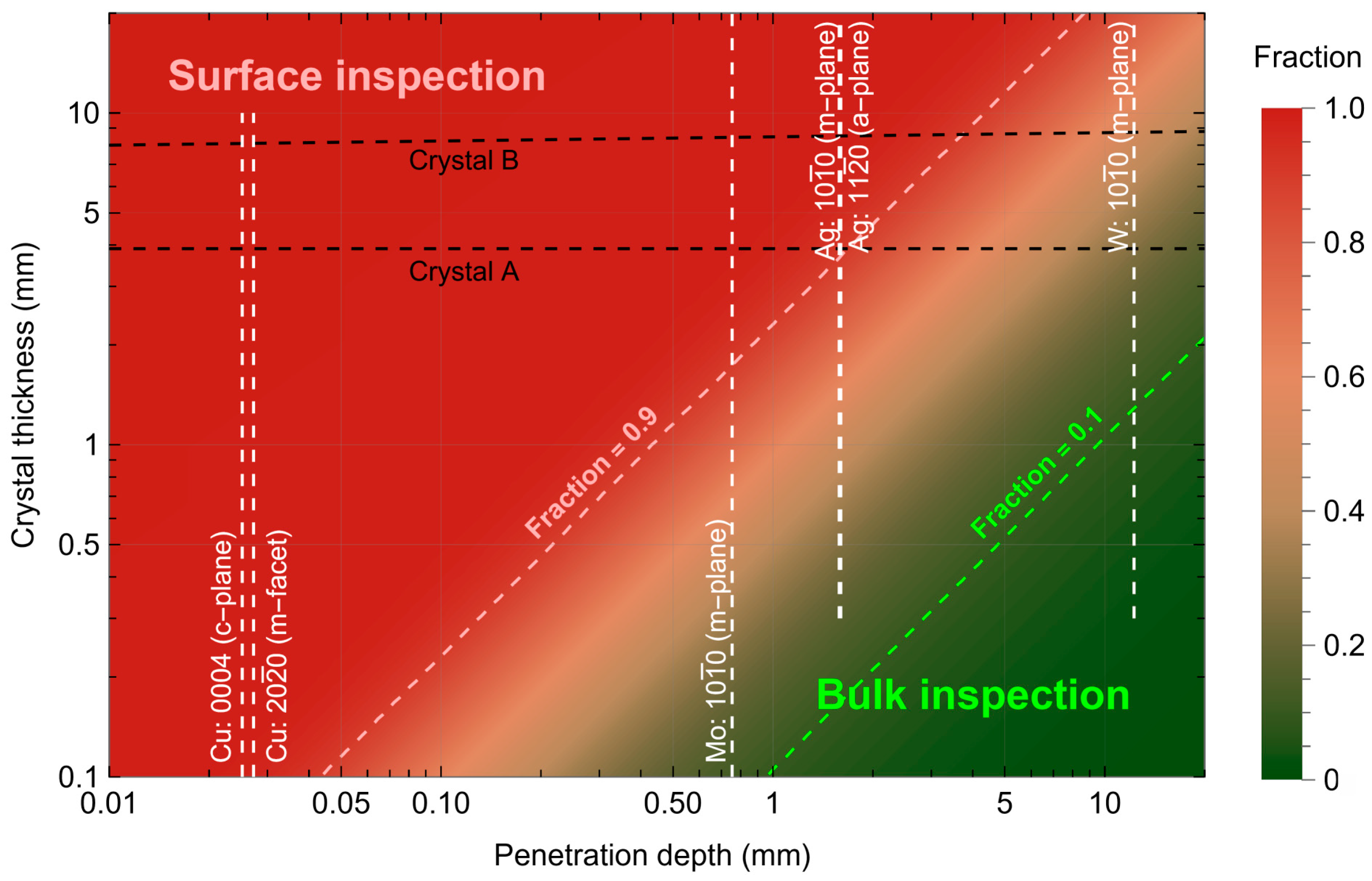
Figure 1. Lambert–Beer fraction x = 1 exp t p of X-rays with respect to crystal thickness t and penetration depth p. The fraction lines x = 0.9 and x = 0.1 separate the surface (red) and bulk (green) inspection area, respectively. Penetrations for reflections of interest and crystal thicknesses in this work are shown as labeled dashed lines.
Crystals 15 00449 g001
Figure 2. Core of the growth setup: AlN crystal grown on a floating seed with source material inside a crucible.
Crystals 15 00449 g002
Figure 3. (a) Laue diffraction setup. The screen can be set in focused or de-focused position at the scattering angle 2 θ Mapping is performed stepping the sample perpendicular to the source beam. (b) Laue spots of the m-plane and a-plane reflections on the screen in the focused measurement condition (left) and the m-plane Laue reflection spot in the de-focused measurement condition for crystal A. (c) The Gaussian line profile of the focused diffraction spot at the indicated position in (b).
Crystals 15 00449 g003
Figure 4. Schematic setup of measurement modes for X-ray topography. (a) Back-reflection geometry and (b) Lang transmission geometry uses a macro-slit of approximately 2 mm. (c) A micro-slit of 37 µm is used for section topography. The Bragg angle θ B is indicated in each panel.
Crystals 15 00449 g004
Figure 5. Bending of the c-plane: lattice shape of (a) crystal A and (b) crystal B for N- (left) and Al-face (right). Dashed lines show the borders of the crystals.
Crystals 15 00449 g005
Figure 6. Panels (a) and (b) show X-ray topographs in symmetric back-reflection geometry for all surfaces of crystal A and B, including the m-facets. The reciprocal lattice vector is always perpendicular to each image. Adjacent surfaces are indicated by connector symbols. Enlargements in (c) show a threading dislocation cluster marked in (a) by (i) on the N-face and by (ii) on the Al-face. Topographs in (d) show enlargements of basal-plane dislocation clusters on the m-facet marked by (iii) and (iv) in (a). Panel (e) shows enlarged single-threading dislocations appearing as elliptic dark spots. Special features marked by red Greek letters are explained in the text.
Crystals 15 00449 g006
Figure 7. Threading dislocation density maps of seed wafer (a), N-face (b), and Al-face (c) of crystal A. Dark spots are the identified threading dislocations. The red dashed line shows the seed boundary on the N-face of crystal A. The enlargements (d,e) show the defect density in the lateral-grown material beyond the seed.
Crystals 15 00449 g007
Figure 8. (a) Lang transmission topograph of the 10 1 ¯ 0 reflection (m-plane). The threading dislocation cluster and basal plane dislocation clusters of interest are marked by a blue and red square and enlarged in (b) and (c), respectively. The panels (i) to (iii) show topographs of three lattice vector orientations of the m-plane (green arrow) and the three panels (iv) to (vi) for the a-plane, corresponding to the pictograms in Figure 10. The arrows aligned as triangles in topographs (b) (i), (ii), and (iii) show the m-plane family. The red arrow is perpendicular to the respective lattice plane vector. Dislocation clusters marked by colored circles in (c) are discussed in the text with respect to their visibility.
Crystals 15 00449 g008
Figure 9. The first row (ad) shows Laue diffraction mappings for crystal A, and the second row (eh) for crystal B. The first column shows reflection images of de-focused Laue transmission, whereas the other columns show the parameter mappings extracted from the Pseudo-Voigtian fit of the focused Laue diffraction reflections. Circles indicate cluster X and Y in crystal A, discussed in the text. Red dashed lines show areas of high tensil stress in crystal B.
Crystals 15 00449 g009
Figure 10. Visibility of line dislocations in topographs for Burgers vectors (columns) and line vectors (rows) represented as pictograms for the six reflections used in this work. The direction of the lattice vector under consideration is shown in the upper-left entry of this table. Red means the non-visibility of a dislocation, while green means that it is visible. Square and disk symbols represent edge and screw dislocation, respectively. Gray circles in squares present mixed dislocations where no extinction rule is applicable.
Crystals 15 00449 g010
Figure 11. Nine image sequences of re-sliced section topography images. The sequence starts at the Al-face (i) to the N-face (ix). The corresponding video is shown in the Supplementary Material (Video S1). The purple thick dashed line shows the border of the seed, while the thin red dashed line presents the lateral growth front. The generation of dislocations of interest is marked by circles, and the colors correspond to the clusters shown in Figure 8c. Inset 1 shows dissolution of a cluster and inset 2 details the dynamical diffraction fringes. Contrasts of both insets have been optimized for visualization.
Crystals 15 00449 g011
Table 1. Selected growth parameters and crystal thickness for crystals A and B.
Ambient PressureGrowth
Temperature
Axial Temp
Gradient
Growth
Rate
Growth Time Crystal Thickness
crystal A~850 mbar~2500 Klow37 µm/h92 h3.9 mm
crystal Bhigh119 µm/h63 h8 mm
Table 2. X-ray source parameters, characteristic wavelengths of the anode material, and resulting absorption coefficient and penetration depth for AlN.
Anode
Material
X-Ray
Power
Characteristic Wavelength 1Absorption
Coefficient 2
Penetration
Depth 3
Copper (Cu)1200 W1.54056 Å114.0 cm−188 µm
Molybdenum (Mo)1200 W0.70930 Å13.2 cm−1760 µm
Silver (Ag)780 W0.55941 Å6.2 cm−11610 µm
Tungsten (W)500 W0.20901 Å0.8 cm−112,260 µm
1 Characteristic Kα1 line for the anodes was taken from [26]. 2 Calculated from NIST database [27]. 3 For normal incidence and thus a maximum value.
Table 3. Sample surface, lattice planes, and reflection conditions for surface and bulk inspection. The surface facets are measured in a symmetric back-reflection geometry. The reflection indices and anode materials are given. Bragg angles are calculated using the average lattice parameters from [29].
SurfaceLattice PlaneReflection IndexBragg AngleAnode
Surface inspection (back-reflection geometry)
N-face/Al-facec-plane 0001 0004 38.2212°Cu
m-facetsm-plane 10 1 ¯ 0 20 2 ¯ 0 34.8891°Cu
a-facetsa-plane 11 2 ¯ 0 11 2 ¯ 0 29.6933°Cu
Bulk inspection (transmission geometry)
N-face upm-plane 10 1 ¯ 0 10 1 ¯ 0 5.9609°Ag
N-face upa-plane 11 2 ¯ 0 11 2 ¯ 0 10.3624°Ag
N-face upm-plane 10 1 ¯ 0 10 1 ¯ 0 2.23°W
Table 4. Principal curvature radii of the saddle-shaped c-plane for crystals A and B of the N-face and Al-face.
N-FaceAl-Face
r 1   @   d 1 r 2   @   d 2 r 1   @   d 1 r 2   @   d 2
crystal A 50 m 48 m 32 m 29 m
crystal B 51 m 29 m 20 m
Table 5. Topograph quality indicators for the surface, integrated bulk inspection, and three-dimensional section topography.
QualifiersSurface InspectionBulk Inspection
Integrated Bulk3D Section Topography
performancefasttime-consumingvery time-consuming
crystal thicknessindependentenergy dependentenergy dependent
dislocation contentonly at surface, threading screw dislocationsfull dislocation
networks
full trajectory
of line dislocation
topograph resolutioncamera dependentcamera dependentin expense of time
mappingsfull crystalfull crystalsmall parts
Disclaimer/Publisher’s Note: The statements, opinions and data contained in all publications are solely those of the individual author(s) and contributor(s) and not of MDPI and/or the editor(s). MDPI and/or the editor(s) disclaim responsibility for any injury to people or property resulting from any ideas, methods, instructions or products referred to in the content.

