Article

Inelastic Electron Tunneling Spectroscopy of Aryl Alkane Molecular Junction Devices with Graphene Electrodes

Department of Applied Physics, Kyung Hee University, Yongin 17104, Republic of Korea
Crystals 2025, 15(5), 433; https://doi.org/10.3390/cryst15050433
Submission received: 3 April 2025 / Revised: 28 April 2025 / Accepted: 30 April 2025 / Published: 1 May 2025
(This article belongs to the Special Issue Advances in Multifunctional Materials and Structures)

Abstract

:
We present a comprehensive vibrational spectroscopic analysis of vertical molecular junction devices constructed using single-layer graphene electrodes separated by an aryl alkane monolayer. In this work, inelastic electron tunneling spectroscopy (IETS) is employed to probe molecular vibrations within the junction, providing an in situ fingerprint of the molecules. Graphene has emerged as a promising electrode material for molecular electronics due to its atomically thin, mechanically robust nature and ability to form stable contacts. However, prior to this study, the vibrational spectra of molecules in graphene-based molecular junctions had not been fully explored. Here, we demonstrate that vertically stacked graphene electrodes can be used to form stable and reproducible molecular junctions that yield well-resolved IETS signatures. The observed IETS spectra exhibit distinct peaks corresponding to the vibrational modes of the sandwiched aryl alkane molecules, and all major features are assigned through density functional theory calculations of molecular vibrational modes. Furthermore, by analyzing the broadening of IETS peaks with temperature and AC modulation amplitude, we extract intrinsic vibrational linewidths, confirming that the spectral features originate from the molecular junction itself rather than extrinsic noise or instrumental artifacts. These findings conclusively verify the presence of the molecular layer between graphene electrodes as the charge transport pathway and highlight the potential of graphene–molecule–graphene junctions for fundamental studies in molecular electronics.

1. Introduction

Molecular electronics aims to create molecular junction devices (MJDs) whose current–voltage relationships exhibit characteristics of conventional or novel electronic behaviors based on component molecules [1,2,3,4,5,6]. MJDs are typically constructed by self-assembling molecular monolayers between top and bottom metallic thin films that serve as electrode materials [1,2]. This horizontal junction arrangement usually involves depositing top metal electrodes onto delicate molecular monolayers through the evaporation process, which can create conductive filaments, resulting in short circuits. Extensive statistical analyses of MJDs made by direct evaporation of top metal electrodes have demonstrated very poor yields of working devices, often below only a few percent [7,8], highlighting the need for alternative methodologies. Consequently, various approaches have been developed to avoid filamentary paths and severe damage to molecular layers caused by evaporated metal atoms, including non-evaporative electrode systems such as conductive polymers (PEDOT:PSS) [8], Ga-based liquid metals (EGaIn) [9], or a direct metal transfer technique [10]. In recent years, single-layer graphene has attracted significant attention as an electrode material for molecular junctions [2,5,7]. Graphene offers exceptional mechanical strength, chemical stability, and electrical conductivity, all in an atomically thin, flexible form [5]. Unlike bulk metal electrodes, graphene can form π–π stacking or covalent bonds with aromatic molecules, enabling a stable and well-defined contact at the molecule–electrode interface [7]. For example, aryl diazonium chemistry can be used to graft molecular layers onto a graphene surface via the formation of robust covalent carbon–carbon bonds [7]. Graphene-based junctions thus provide a promising platform for studying intrinsic charge transport properties of molecular monolayers without the complications of metal penetration or filamentary shorts. Moreover, a graphene top electrode can gently interface with a molecular layer through van der Waals interactions, potentially preserving the integrity of the molecular assembly while still ensuring good electrical contact.
Inelastic electron tunneling spectroscopy (IETS) is a powerful technique for characterizing molecular junctions, as it provides a vibrational fingerprint of the molecules participating in charge transport [11,12,13]. In an IETS measurement, a small AC modulation is superimposed on the bias voltage and the second derivative of the current (I)–voltage (V) curve is recorded, typically at cryogenic temperatures to reduce thermal broadening. Peaks (or dips) in the IETS spectrum occur at characteristic voltages corresponding to the energies of vibrational modes of the molecule. Over the past few decades, IETS has been extensively applied to molecular junctions with conventional metal electrodes [1,11,12]. These studies have provided insight into the vibrational modes of various molecular systems and their coupling to electron transport. However, comprehensive IETS investigations of molecular junctions with two-dimensional materials like graphene as electrodes have remained largely unexplored.
Here, we report the detailed vibrational spectroscopy study of a graphene–molecule–graphene-tunneling junction. We focus on vertical junctions comprising an aryl alkane monolayer covalently attached to a bottom graphene electrode and physically contacted by a top graphene electrode. We demonstrate that this all-carbon electrode junction architecture yields stable devices with a high fabrication success rate, enabling us to systematically measure IETS spectra. The vibrational features observed in these graphene-based junctions are assigned to specific molecular normal modes with the support of density functional theory (DFT) calculations and comparisons to known vibrational data. Furthermore, by examining how the IETS peak widths change with temperature and modulation voltage, we differentiate intrinsic molecular signals from extrinsic broadening effects. Overall, our results verify that charge transport in these junctions occurs through the intended molecular layer and highlight the unique advantages of graphene electrodes for fundamental studies in molecular electronics.

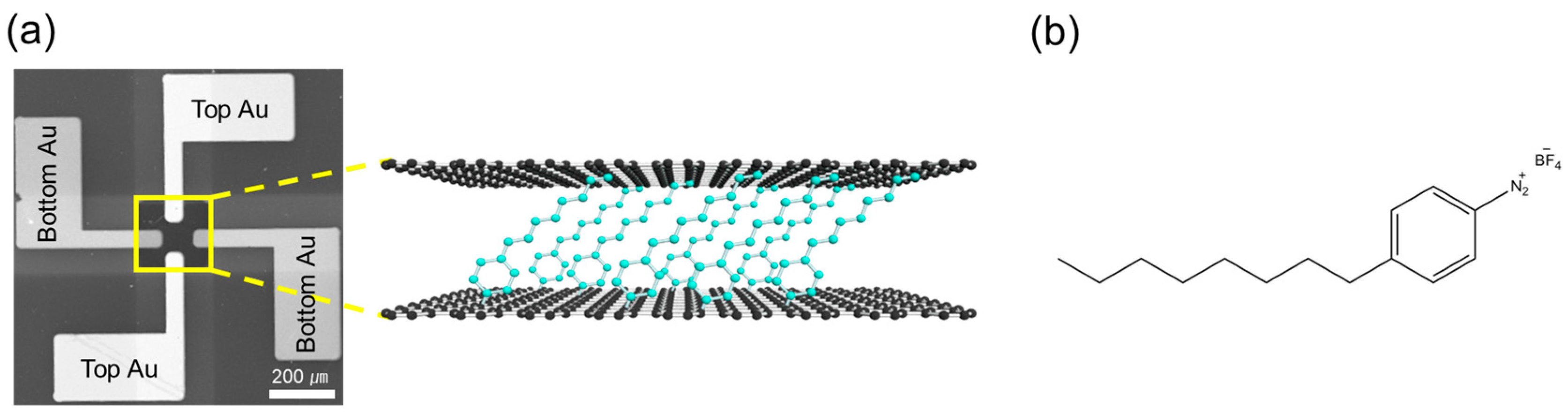
2. Materials and Methods

We used a single-layer graphene (purchased from Graphene Square Inc. Seoul, Korea), which was prepared by a chemical vapor deposition (CVD) method on copper foil and subsequently transferred to the device substrate (this detail was described in the Supplementary Materials). Two pronounced peaks from Raman spectroscopy measurement for pristine graphene layer appeared at G band (1582 cm−1) and 2D band (2675 cm−1) (Figure S1 in the Supplementary Materials), consistent with previously reported results [1]. The large intensity ratio (~2.6) of 2D band over G band was characteristic of single-layer graphene [8]. The aryl alkane molecules were grafted onto the pre-patterned bottom graphene electrode via a well-known diazotization reaction of sp2-hybridized carbon systems [7], which creates robust covalent bonds between the aryl alkane molecules and graphene electrodes. In contrast, the upper end of the aryl alkane layers was in contact with the electrode through van der Waals interactions. Figure 1 displays a scanning electron microscopy (SEM) image of the MJDs and the device illustration in cross-section view. For molecular grafting, 4-octyl-benzenediazonium tetrafluoroborate (purchased from Tokyo Chemical Industry, Tokyo, Japan) was used, and its chemical structure is displayed in Figure 1b. To verify the formation of the molecular monolayer on the graphene surface, we performed atomic force microscopy (AFM) characterization. Representative AFM height profile line-scans on the graphene substrate before and after molecular grafting are shown in Figure S2 (in the Supplementary Materials). The observed ~2.0 nm height increase is consistent with the expected thickness of a single monolayer of aryl alkane molecules (in agreement with the molecular length predicted by chemical structure modeling). This confirms the successful assembly of a uniform molecular monolayer on the graphene electrode. The vertical junction arrangement of graphene/molecules/graphene demonstrates excellent stability for successive electrical transport and IETS measurements with high device yield (>80%). SEM images of the completed device revealed an active junction area of approximately 250 × 250 μm2. The detailed fabrication procedure of MJDs with graphene electrodes and additional characterizations are described in the Supplementary Materials.
Completed devices were mounted in a chip carrier and characterized in a cryogenic probe system. For all inelastic tunneling spectroscopy measurements, the samples were cooled to 4.2 K in a liquid helium dewar to minimize thermal noise. The device was wired in a two-terminal configuration using the graphene electrodes as contacts. A computer-controlled source measure unit with 16-bit digital-to-analog converters was used to apply bias voltage across the junction, and the resultant current was measured with a low-noise current preamplifier (Ithaco 1211, IL, USA) connected to a digital multimeter. To obtain IETS data, a small AC-voltage modulation (7.8 mV root-mean-square at 1033 Hz) was added to the DC bias. The differential conductance (dI/dV) and the second derivative (d2I/dV2) signals were acquired using lock-in detection techniques. In practice, we directly measured the second-harmonic response of the current under the applied AC modulation, which is proportional to d2I/dV2. A lock-in amplifier with a 1 s time constant was used to amplify and record this second-harmonic signal. This setup allows us to capture IETS spectra (d2I/dV2 vs. voltage) with enhanced signal-to-noise by focusing on the AC modulation response. All I(V) and IETS measurements were performed under high-vacuum conditions to prevent sample contamination or frost buildup at cryogenic temperatures.
To aid in interpreting the IETS spectra, density functional theory (DFT) calculations were carried out to compute the vibrational modes of an isolated aryl alkane molecule (corresponding to the monolayer constituent). Geometry optimizations and normal mode analyses were performed using the B3LYP exchange-correlation functional with a 6-311G** basis set. These calculations (executed with the Jaguar quantum chemistry software, v6.5) provided the frequencies and character of vibrational modes for the free molecule. The theoretical vibrational frequency values were later compared with the experimentally observed IETS peak positions. In addition, the literature values from infrared and Raman spectra of similar molecules were consulted to confidently assign each IETS peak to a specific vibrational mode.

3. Results and Discussion

3.1. Elecrical Tranpsort Characterizations

Temperature-dependent I(V) measurements are essential for determining charge transport mechanisms in MJDs [1,5,8]. Figure 2a presents typical I(V) curves of graphene–aryl alkane–graphene junctions, recorded between 4.2 and 120 K. The I(V) data showed no significant temperature dependence, indicating tunneling transport that excludes alternative (thermally activated) mechanisms like hopping conduction or thermionic emission [8,14]. Tunneling charge transport can be further confirmed by examining current as a function of molecular length. For non-resonant tunneling, the current decreases exponentially with increasing molecular length [5]. To study the length-variable transport of the junctions, the semilogarithmic plot of current density (J) (measured at 1 V) against the molecular length (d) is shown in Figure 2b, depending on the number of carbons in alkyl chains. This plot revealed an evident exponential dependency of J on d, according to J ∝ exp(−βd) [8,9], in which the slope of the linear fit shown in Figure 2b yielded the decay coefficient (β). The β value was estimated to be 1.07 per carbon atom (equal to 0.86 Å−1). The error bars denoted the standard deviation of experimentally measured current densities. The β value was reasonably consistent with that observed in the alkyl chains [14]. As a result, the temperature and length-variable electrical transport measurements indicate that the charge transport occurs via tunneling across the aryl alkane monolayers bridging two graphene electrodes. Among approximately 50 completed devices that did not experience fabrication failure, 42 exhibited typical tunneling I(V) characteristics after removing samples that showed open- and short-circuit behavior. These tunneling devices did not significantly degrade over the measurement period.

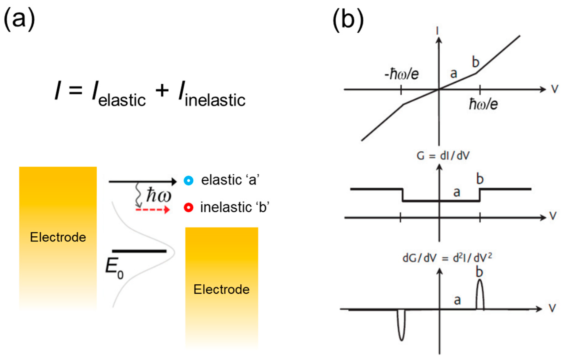
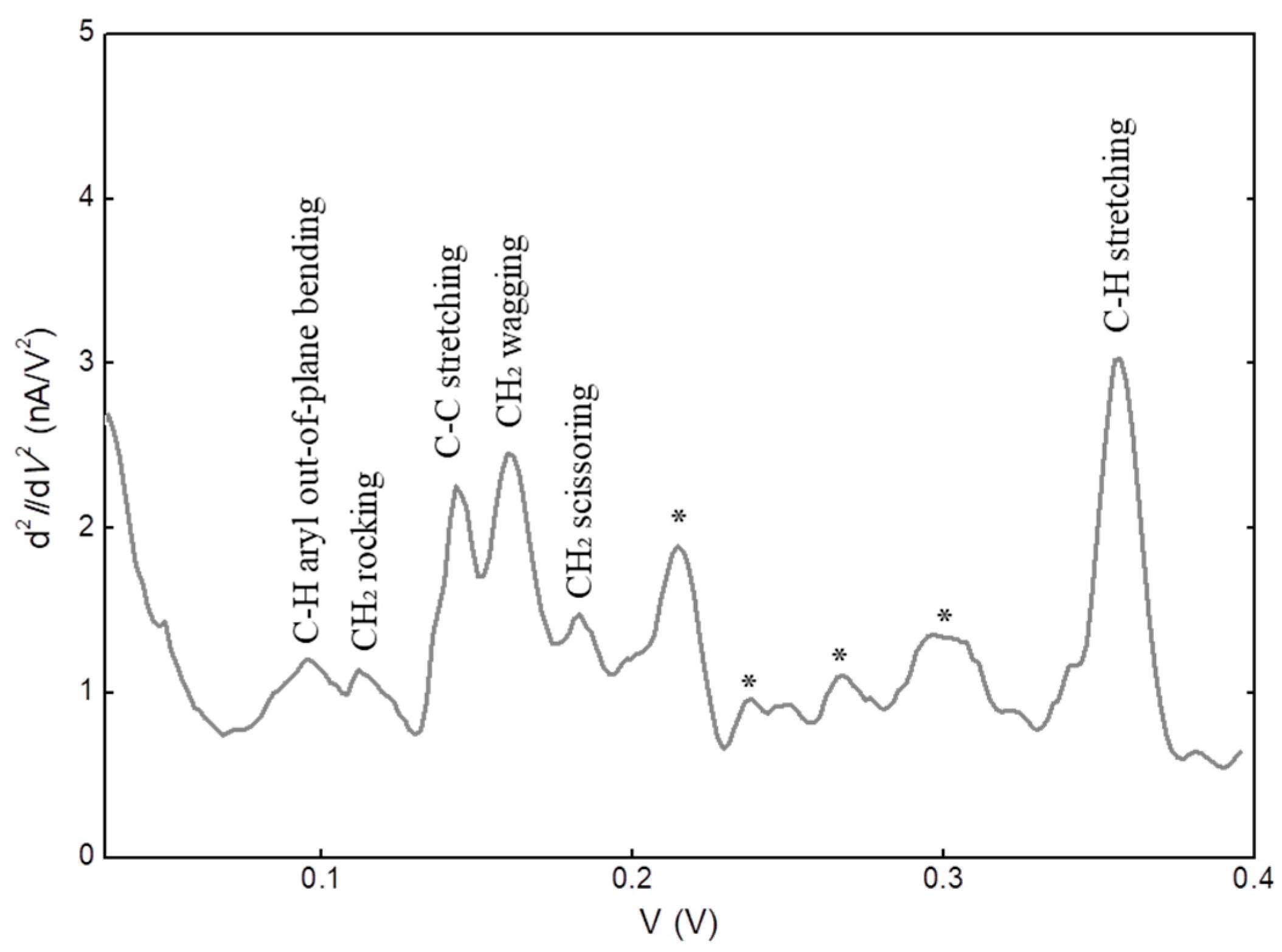
3.2. Inelastic Electron-Tunneling Spectroscopy Measurements

IETS was originally developed by Jaklevic et al. [15] as an electronic method to detect molecules adsorbed onto metal surfaces using scanning tunneling microscopy. This technique has evolved into a valuable tool for analyzing a molecular junction created by modern semiconductor fabrication processes [12,13]. During IETS measurements, the current flowing through MJDs consists of both elastic and inelastic tunneling components [16]. The process is displayed in Figure 3a, where a molecule is positioned between two electrodes with the molecular orbital energy E0 separated from the Fermi level (EF) by several hundred meV. When an external voltage is biased, the chemical potentials between both electrodes become unbalanced, creating a non-resonant tunneling transport window. In elastic tunneling (‘a’), electrons move from an occupied state in one electrode to an empty state in the opposite electrode while maintaining their energy. This results in the current increasing linearly with a low-voltage regime, as depicted in Figure 3b. However, when an inherent mode of vibrational frequency ω exists within the junction, electrons can transfer energy (ħω) to excite this vibration if the applied voltage exceeds the threshold energy (eVħω). Such an inelastic transport mechanism (‘b’) increases the overall probability of tunneling transmission through a molecular barrier. The resulting inelastic current exhibits a characteristic kink at specific voltages, appearing as a step in the graph of differential conductance and as a peak (or dip) in the second derivative plots [16], as shown in Figure 3b. Since inelastic tunneling typically represents only a small fraction of the total current due to electron transit times being much shorter than vibrational oscillator periods, these conductance features are often subtle [11,12]. Hence, we directly acquired the second derivative peaks through a phase-sensitive lock-in technique with enhanced signal-to-noise ratios.
Figure 4 displays the IETS spectrum measured from graphene/aryl alkane/graphene junctions at 4.2 K. The plot of d2I/dV2 against V reveals specific features corresponding to the molecules’ vibrational modes, as described above. An AC modulation technique with lock-in amplification was employed to directly measure a second derivative signal proportional to the d2I/dV2 peak intensity [13,16]. The IETS spectrum of aryl alkane junctions in Figure 4 remained consistent during successive bias sweeps. When molecular vibrations couple with tunneling-charge carriers, they increase inelastic electron-tunneling current, appearing as peaks in d2I/dV2 spectrum. To assist with vibrational mode identification, the density functional theory (DFT) calculation was performed on the free aryl alkane form of the studied molecules (B3LYP/6-311G** level using Jaguar v6.5). Additionally, vibrational modes were assigned by comparing with formerly published infrared, Raman, and other IETS data [17]. The most prominent feature was the C-H stretching mode at 356 mV. Simulation studies using nonequilibrium Green’s function formalism have indicated that the C-H peak intensity may vary depending on the surface-binding geometry. The C-H peak’s full width at half maximum (FWHM) was 17 mV (measured with Gaussian distribution fitting), consistent with theoretical predictions under our measurement conditions [16]. Various lower-energy vibrations between 30~200 mV also appeared at 96, 117, 142, 162, and 183 mV, corresponding to C-H aryl out-of-plane bending, CH2 rocking, C-C stretching, CH2 wagging, and CH2 scissoring modes, which is consistent with the characteristics of aryl alkane molecular structures [18]. The asterisks at 210~300 mV in Figure 4 are most likely associated with stacked top and bottom SLG electrodes or the substrate [18,19], which are not part of the tunnleing barrier in MJDs. These notable peaks assigned to inherent molecular vibrational modes indicate the formation of a strong C−C sp3 bond between the aryl alkane monolayers and graphene electrodes. These comprehensively assigned IETS spectra not only confirm the presence of specific molecules within the graphene electrodes but also demonstrate their direct role in charge transport through these MJDs. Thus, this result suggests that charge tunneling occurs exclusively through the molecules themselves.

3.3. Broadeing of Spectral Linewidths

A crucial validation technique for IETS data involves analyzing how vibrational peak widths broaden in response to temperature changes and AC modulation voltage [20,21]. IETS spectral peak widths comprise an intrinsic linewidth Win plus two broadening mechanisms: thermal broadening (5.4 kBT/e in which T indicates temperature, and kB represents Boltzmann’s constant), caused by Fermi level expansion, and modulation broadening (1.7 Vm, in which Vm is the modulation voltage), resulting from the second harmonic signal detection method. The total FWHM (WFWHM) of a vibrational peak in IETS spectrum can be calculated using the following equation [21,22]:
WFWHM = [(1.7 Vm)2 + (5.4 kBT/e)2 + (Win)2]½
Figure 5 demonstrates the linewidth broadening analysis of the aryl alkane IETS spectrum. Figure 5a illustrates AC modulation broadening for the C-C stretching mode in the IETS spectrum measured at a constant temperature (4.2 K). By fitting the experimental FWHM data to account for theoretical modulation and thermal broadening model (Equation (1)), we determined an intrinsic linewidth (Win) of 4.87 ± 0.73 meV. Figure 5b displays thermal broadening effect of the same C-C stretching peak at fixed modulation (7.8 mV), with reasonable agreement between theoretical predictions (circles) and experimental measurements (squares with error bars). This systematic linewidth analysis confirms that the observed IETS spectrum results from inherent vibrational modes of the component molecules in MJDs with graphene electrodes rather than thermal or instrumental noise.

4. Conclusions

The aryl alkane monolayer was incorporated as a tunneling barrier into graphene/molecule/graphene junctions, where the molecules were covalently self-assembled onto the bottom graphene electrode, whereas the upper end of the aryl alkane monolayers is physically contacted with the top graphene electrode by van der Waals interaction. The vertical arrangement of MJDs with graphene electrodes provided appropriate stability as a testbed for investigating charge transport through molecular monolayers. Fully assigned vibrational spectra were obtained from the aryl alkane MJDs with graphene electrodes using IETS. In addition, the linewidth-broadening analysis demonstrated that the vibrational features in the IETS spectrum originate from the component molecules themselves but not artificial noise signals [23,24,25]. The IETS spectra clearly reflected molecular chemical structures, verifying the formation of stable graphene–molecule contacts.
The insights gained from this study underscore the potential of graphene-based molecular junctions for both fundamental research and future applications. By achieving stable and reproducible molecular junctions with fully assigned vibrational spectra, we pave the way for exploring more complex molecular electronic functionalities using graphene electrodes. As a broader implication, the preservation of clear molecular vibrational signatures in a graphene-based junction indicates that graphene electrodes can be utilized without obscuring the intrinsic molecular behavior. This opens up opportunities to explore other molecular electronic phenomena in such junctions. For example, the gating of molecular orbital energies—a unique effect observed in traditional single-molecule junctions with metal electrodes—could potentially be studied in devices with graphene contacts as well. Our results demonstrate that incorporating graphene as electrodes provides a stable platform for examining molecular properties, combining the advantages of an atomically thin electrode with the ability to perform in situ spectroscopic characterization of the molecule.

Supplementary Materials

The following supporting information can be downloaded at https://www.mdpi.com/article/10.3390/cryst15050433/s1: Figure S1: The fabrication process for creating aryl alkane MJDs with graphene electrodes; Figure S2. Raman spectrum of CVD-grown single-layer graphene transferred to Si/SiO2 substrate; Figure S3: Line profile analysis of atomic force microscopy images.

Funding

This research received no external funding.

Data Availability Statement

Data are contained within the article or Supplementary Materials.

Conflicts of Interest

The author declares no conflicts of interest.

References

  1. Vilan, A.; Aswal, D.; Cahen, D. Large-Area, Ensemble molecular electronics: Motivation and challenges. Chem. Rev. 2017, 117, 4248–4286. [Google Scholar] [CrossRef] [PubMed]
  2. Yuan, M.; Qiu, Y.; Gao, H.; Feng, J.; Jiang, L.; Wu, Y. Molecular electronics: From nanostructure assembly to device integration. J. Am. Chem. Soc. 2024, 146, 7885–7904. [Google Scholar] [CrossRef]
  3. Yu, C.J.; Von Kugelgen, S.; Laorenza, D.W.; Freedman, D.E. A molecular approach to quantum sensing. ACS Cent. Sci. 2021, 7, 712–723. [Google Scholar] [CrossRef]
  4. Moreno-Pineda, E.; Wernsdorfer, W. Measuring molecular magnets for quantum technologies. Nat. Rev. Phys. 2021, 3, 645–659. [Google Scholar] [CrossRef]
  5. Chen, H.; Fraser Stoddart, J. From molecular to supramolecular electronics. Nat. Rev. Mater. 2021, 6, 804–828. [Google Scholar] [CrossRef]
  6. Al-Owaedi, O.A.; Najeeb, H.N.; Aldulaimi, A.K.O.; Alwan, N.H.; Ali, M.S.; Dwech, M.H.; AL-Da’amy, M.A. Thermoelectric signature of d-orbitals in tripod-based molecular junctions. Mater. Adv. 2024, 5, 9781–9791. [Google Scholar] [CrossRef]
  7. Jia, C.; Guo, X. Molecule–electrode interfaces in molecular electronic devices. Chem. Soc. Rev. 2013, 42, 5642–5660. [Google Scholar] [CrossRef]
  8. McCreery, R.L.; Bergren, A.J. Progress with molecular electronic junctions: Meeting experimental challenges in design and fabrication. Adv. Mater. 2009, 21, 4303–4322. [Google Scholar] [CrossRef] [PubMed]
  9. Wan, A.; Jiang, L.; Sangeeth, C.S.S.; Nijhuis, C.A. Reversible soft top-contacts to yield molecular junctions with precise and reproducible electrical characteristics. Adv. Funct. Mater. 2014, 24, 4442–4456. [Google Scholar] [CrossRef]
  10. Li, T.; Bandari, V.K.; Schmidt, O.G. Molecular electronics: Creating and bridging molecular junctions and promoting its commercialization. Adv. Mater. 2023, 35, 2209088. [Google Scholar] [CrossRef]
  11. Kim, Y.; Chang, S.W. Inelastic electron tunneling spectroscopy: Investigation of bulk dielectrics and molecules. IEEE Trans. Electron Devices 2021, 68, 1411–1419. [Google Scholar] [CrossRef]
  12. Ngabonziza, P.; Wang, Y.; van Aken, P.A.; Maier, J.; Mannhart, J. Inelastic electron tunneling spectroscopy at high-temperatures. Adv. Mater. 2021, 33, 2007299. [Google Scholar] [CrossRef] [PubMed]
  13. Cao, Y.; Austin, D.; Switzer, E.D.; Rowen, J.F.; Sander, W.; Rahman, T.S.; Morgenstern, K. Inelastic electron tunneling spectroscopy as a probe of electronic coupling at a molecule-metal interface. Phys. Rev. B 2025, 111, 115426. [Google Scholar] [CrossRef]
  14. Jeong, H.; Kim, D.; Kwon, H.; Hwang, W.-T.; Jang, Y.; Min, M.; Char, K.; Xiang, D.; Jeong, H.; Lee, T. Statistical investigation of the length-dependent deviations in the electrical characteristics of molecular electronic junctions fabricated using the direct metal transfer method. J. Phys. Condens. Matter 2016, 28, 94003. [Google Scholar] [CrossRef]
  15. Jaklevic, R.C.; Gaerttner, M.R. Inelastic electron tunneling spectroscopy. experiments on external doping of tunnel junctions by an infusion technique. Appl. Surf. Sci. 1978, 1, 479–502. [Google Scholar] [CrossRef]
  16. Kirtley, J.; Scalapino, D.J.; Hansma, P.K. Theory of vibrational mode intensities in inelastic electron tunneling spectroscopy. Phys. Rev. B 1976, 14, 3177. [Google Scholar] [CrossRef]
  17. Kim, Y.; Song, H. Investigation of molecular junctions with inelastic electron tunneling spectroscopy. Appl. Spectrosc. Rev. 2016, 51, 603–620. [Google Scholar] [CrossRef]
  18. Song, H.; Kim, Y.; Ku, J.; Jang, Y.H.; Jeong, H.; Lee, T. Vibrational spectra of metal-molecule-metal junctions in electromigrated nanogap electrodes by inelastic electron tunneling. Appl. Phys. Lett. 2009, 94, 103110. [Google Scholar] [CrossRef]
  19. Rao, R.; Podila, R.; Tsuchikawa, R.; Katoch, J.; Tishler, D.; Rao, A.M.; Ishigami, M. Effects of layer stacking on the combination Raman modes in graphene. ACS Nano 2011, 5, 1594–1599. [Google Scholar] [CrossRef]
  20. Song, H.; Kim, Y.; Jang, Y.H.; Jeong, H.; Reed, M.A.; Lee, T. Observation of molecular orbital gating. Nature 2009, 462, 1039–1043. [Google Scholar] [CrossRef]
  21. Wang, W.; Lee, T.; Kretzschmar, I.; Reed, M.A. Inelastic electron tunneling spectroscopy of an alkanedithiol self-assembled monolayer. Nano Lett. 2004, 4, 643–646. [Google Scholar] [CrossRef]
  22. Reed, M.A. Inelastic electron tunneling spectroscopy. Mater. Today 2008, 11, 46–50. [Google Scholar] [CrossRef]
  23. Fereiro, J.A.; Pecht, I.; Sheves, M.; Cahen, D. Inelastic Electron Tunneling Spectroscopic Analysis of Bias-Induced Structural Changes in a Solid-State Protein Junction. Small 2021, 17, 2008218. [Google Scholar] [CrossRef] [PubMed]
  24. Kesarwani, S.; Misra, S.; Saha, D.; Della Rocca, M.L.; Roy, I.; Ganguly, S.; Mahajan, A. Simplified inelastic electron tunneling spectroscopy based on low-noise derivatives. Sci. Rep. 2022, 12, 19216. [Google Scholar] [CrossRef]
  25. Thomas, A.; Syamadas, S.; Jinesh, K.B. Molecular level inelastic electron tunneling spectroscopy of protoporphyrin using scanning tunneling microscope. Spectrochim. Acta A Mol. Biomol. Spectrosc. 2025, 337, 126126. [Google Scholar] [CrossRef]
Figure 1. (a) The SEM image (left) of MJDs and the device schematic in a cross-section view. Aryl alkane molecules are sandwiched between single-layer graphene (SLG) electrodes. (b) Chemical structure of 4-octyl-benzenediazonium tetrafluoroborate.
Crystals 15 00433 g001
Figure 2. (a) The temperature-variable I(V) plot of graphene/aryl alkane/graphene MJDs, recorded between 4.2 and 120 K. (b) The semilogarithmic plot of length-dependent current density. The current densities were measured at 1 V. The molecules with different lengths are denoted by the number of carbons in alkyl chains as C8, C10, and C12, respectively.
Crystals 15 00433 g002
Figure 3. (a) A schematic and energy-band diagram of graphene/aryl alkane/graphene MJDs. A molecular energy level (E0) with its broadening is in non-resonant condition. Total tunneling currents are represented as the sum of elastic (‘a’) and inelastic (‘b’) ones. ℏω indicates molecular vibrational energy. (b) Inelastic tunneling caused by molecular vibrational modes results in increasing current, which is shown as a step in the dI/dV versus V(applied voltage) plot and a peak in the d2I/dV2 versus V plot. The second derivative (d2I/dV2) signals are directly measured by a standard lock-in technique to improve signal-to-noise ratios.
Crystals 15 00433 g003
Figure 4. IETS spectrum of graphene/aryl alkane/graphene MJDs measured at 7.8 mV modulation voltage and 4.2 K. Each peak is tagged with the assignment of a vibrational mode. The peaks with asterisks (210~300 mV) are most likely due to stacked graphene layers or the substrate effect.
Crystals 15 00433 g004
Figure 5. IETS spectral linewidths of C-C stretching mode measured at (a) different AC modulation voltages and (b) variable temperatures. The experimental FWHM data (squares with error bars) are fitted to theoretical linewidths (from Equation (1)), which indicate (a) blue line and (b) blue circles. Error bars are obtained by Gaussian fitting of FWHM.
Crystals 15 00433 g005
Disclaimer/Publisher’s Note: The statements, opinions and data contained in all publications are solely those of the individual author(s) and contributor(s) and not of MDPI and/or the editor(s). MDPI and/or the editor(s) disclaim responsibility for any injury to people or property resulting from any ideas, methods, instructions or products referred to in the content.

