Article

The Influence of Structural Design on the Electronic Properties of a Frisch Grid Cadmium Zinc Telluride Detector by a Finite Element Method

1
School of Materials Science and Engineering, Shanghai University, Shanghai 200444, China
2
Nanjing Engineering Branch, Jiangsu Union Technical Institute, Nanjing 211135, China
3
State Key Laboratory of Materials for Advanced Nuclear Energy, Shanghai 200444, China
4
Zhejiang Institute of Advanced Materials, Shanghai University, Jiashan 314113, China
5
Shanghai Collaborative Innovation Center of Intelligent Sensing Chip Technology, Shanghai 201900, China
*
Authors to whom correspondence should be addressed.
Crystals 2025, 15(4), 361; https://doi.org/10.3390/cryst15040361
Submission received: 20 March 2025 / Revised: 7 April 2025 / Accepted: 8 April 2025 / Published: 15 April 2025
(This article belongs to the Section Inorganic Crystalline Materials)

Abstract

:
Cadmium zinc telluride (CZT) detectors have the advantages of high detection efficiency and good energy resolution, which are widely used in the fields of X-ray detection, environmental monitoring and nuclear radiation detection. The Frisch grid structure is used more often in the preparation of detectors because of its good unipolarity and simple structure. In this paper, the effects of changing the gate position, width and relative dielectric constant on the electrical properties of Frisch grid CZT detectors, such as potential, weight potential, electric field distribution and charge collection efficiency, are simulated in detail by the finite element method. From the simulation results, the optimisation of the performance of the Frisch grid detector is mainly based on minimising the distance between the gate and anode within a reasonable interval, increasing the area of the Frisch grid and selecting a material with a high relative permittivity for the fabrication of the Frisch grid. The research work contributes to the development of CZT detectors.

1. Introduction

Cadmium zinc telluride (CZT) has a wide bandgap and a high atomic number, which make it attractive for room-temperature semiconductor detector applications. Over the past two decades, many efforts have been made to study the crystal growth, post-growth annealing, and device fabrication of CZT crystals [1]. Detector-grade CZT crystals are required to facilitate their applications in the fields of non-proliferation, national security, and medical imaging. CZT detectors come in various structures, each with specific structural compositions and performance characteristics tailored to different applications. Standard CZT detectors typically consist of a CZT crystal layer with metal electrodes, offering high detection efficiency and excellent energy resolution suitable for general radiation detection tasks [2]. At present, researchers have not yet mastered the growth technology of high-quality and large-sized CZT crystals, and the yield of CZT single crystals is very low [3]. This results in commercial CZT crystal detectors having a very small size, typically around 2 cm3. In order to increase the effective working area of the detector, it is usually necessary to assemble a single CZT detector into an array detector. In addition, the hole mobility of CZT single crystal detectors is very low, which can reduce the spectral resolution of CZT detectors [4]. When a detector is irradiated with high doses of X-rays or gamma rays, polarisation effects occur, which influence the work of the detector greatly [5]. So, single-charge-carrier detectors, such as a small pixel effect detector, the co-planar grid detector, and the virtual Frisch grid detector, are studied to overcome the deleterious effects of incomplete hole collection upon γ-ray energy resolution [6].
Many research institutions, such as the Department of Non-proliferation and National Security of Brookhaven National Laboratory (BNL), have studied virtual Frisch grid (VFG) detectors in the past two decades for imaging or gamma ray detections [7]. CZT detectors with a Frisch grid incorporate a grid structure on the crystal surface, aimed at enhancing energy resolution and spatial resolution and reducing response time, making them particularly suitable for high-resolution imaging applications [8]. Interdigitated electrode CZT detectors feature electrodes arranged in an interleaved pattern, reducing the dead layer effect and enhancing detection efficiency, especially for low-dose radiation detection. Conversely, ring electrode CZT detectors utilise ring-shaped electrodes on the crystal surface to improve energy resolution, making them well-suited for detecting high-energy radiation such as γ-rays due to their high detection efficiency [9]. Each structure of CZT detectors offers distinct advantages, making them crucial components in various radiation detection scenarios. The goal of the present effort is to use the finite element method to simulate the influence of Frisch grid structural characteristic parameters on detector performance. Through these simulations, the device structure of the CZT detector will be optimised and the detector performance will be improved.

2. Method

In this research, we utilise the commercial software COMSOL Multiphysics, version 6.2. The simulation modules we use are the Electrostatics module and the Coefficient Form Partial Differential Equation (PDE) module. Here, the Electrostatics module is used to simulate the device’s electric potential and weighting potential distribution; the Coefficient Form PDE module is used to establish the device’s charge induction efficiency equation, into which the electric potential and weighting potential distributions are substituted to simulate the charge induction efficiency of the device.

2.1. Derivation of Electric Fields, Potentials and Weight Potential

The application of an external electric field at the detector electrodes causes the electrons in them to move towards the anode and the holes towards the cathode. The electric field E and potential in the detector can be calculated by Gauss’s law and Poisson’s equation [10].
  E = ρ ε ,
E = φ 2 φ = ρ ε ,
where E is the electric field, φ is the potential, ρ is the charge density, and ε is the dielectric constant. The carrier drift velocity v depends on the electric field and the carrier mobility μ [10].
ν = μ E .

2.2. Derivation of the Charge Induced Efficiency (CIE)Formula

In semiconductor detectors, charge induction efficiency (CIE) is usually used to describe charge transport and charge pulse distribution. The charge induction efficiency is the ratio of the actual induced charge on a pixel electrode of the detector to the total theoretical charge generated by the interaction of incident photons with the detector material. It is a dynamic parameter that is spatially and temporally dependent, reflecting the efficiency with which charge carriers (such as electrons) drift, diffuse, and are collected within the detector. Its calculation is based on physical processes such as electric field distribution, carrier mobility, and trapping effects and is obtained by solving the adjoint electron continuity equation. It is a core parameter for evaluating how a CZT/CdTe detector converts incident photon energy into detectable electrical signals. Its definition and distribution are directly related to the detector’s energy resolution, signal-to-noise ratio, spatial resolution, and time response characteristics. This characterisation can be experimentally validated using time-resolved microwave conductivity measurements combined with spatially resolved photoluminescence mapping. We believe that excess carriers satisfy the following continuum equation [11]:
n t = D 2 n μ n φ n τ + S r , t .
Here, n is the concentration of carriers, μ is carrier mobility, D is diffusion coefficient, φ is applied voltage, τ is carrier lifetime, S is generate item, and D and μ are coordinate-independent quantities, where the first term of the right equation describes the diffusion of carriers in the semiconductor, the second term describes the migration of carriers in the semiconductor, the third term describes the effect of impurities and defects in the semiconductor on carrier capture, and the last term describes the effect of X-ray incidence on the generation of carriers. The carrier generation term can be set as a pulse of unit point charge S r , t = δ r r , t t ; then, Green’s function satisfies the homogeneous boundary condition g ( r , t | r , t ) and satisfies g ( r , t | r , t ) = 0, for t < t , which is a solution of Equation (4) [12] as follows:
g t = D 2 g μ g φ g τ + δ r r , t t .
g r , t | r , t   gives the material concentration in the detector at any time greater than t and at any position. Using the Shockley–Ramo theorem, it is easy to show that for a spatially distributed charge q with a concentration of g and a volume of Ω, the amount of induced charge at a specific electrode is [12,13] as follows:
q i n d = q μ 0 t * d t Ω g r , t | r , t φ r ψ r d 3 r ,
where ψ is the weight potential of the target electrode.
Charge induction efficiency is defined as the ratio of the charge induced at a given electrode to the charge produced by the interacting X-rays [11].
η r , t = q i n d q = μ 0 t * d t Ω g r , t | r , t φ r ψ r d 3 r .
In fact, the direct calculation of η is more difficult because all possible positions, r 0 , which X-rays interact with in the detector volume, must be calculated in g ( r , t | r , t ) . Prettyman proposed an efficient method to calculate the induced signal on the electrode of an electric charge generated at any time, at any location, by solving a single equation dependent on time. Using the adjoint definition of differential operators, it is easy to write the adjoint formula of Formula (4) [12].
n ˜ t = D 2 n ˜ + μ φ n ˜ n ˜ r + S ˜ .
We can arbitrarily choose the adjoint generation terms in Formula (8); for example, let S ˜ = μ φ ψ ; then, the adjoint equation becomes as follows:
n ˜ t = D 2 n ˜ + μ φ n ˜ n ˜ r + μ φ ψ .
Prettyman proved that in appropriate initial and boundary conditions, the solution of the adjoint Equation (9) is equivalent to Equation (7), which is the CIE definition [12,14,15].
η r , t = n ˜ r , t
Thus, by solving a single adjoint Equation (9), the charge-induced efficiency diagram of a specific electrode at any time and position can be obtained.

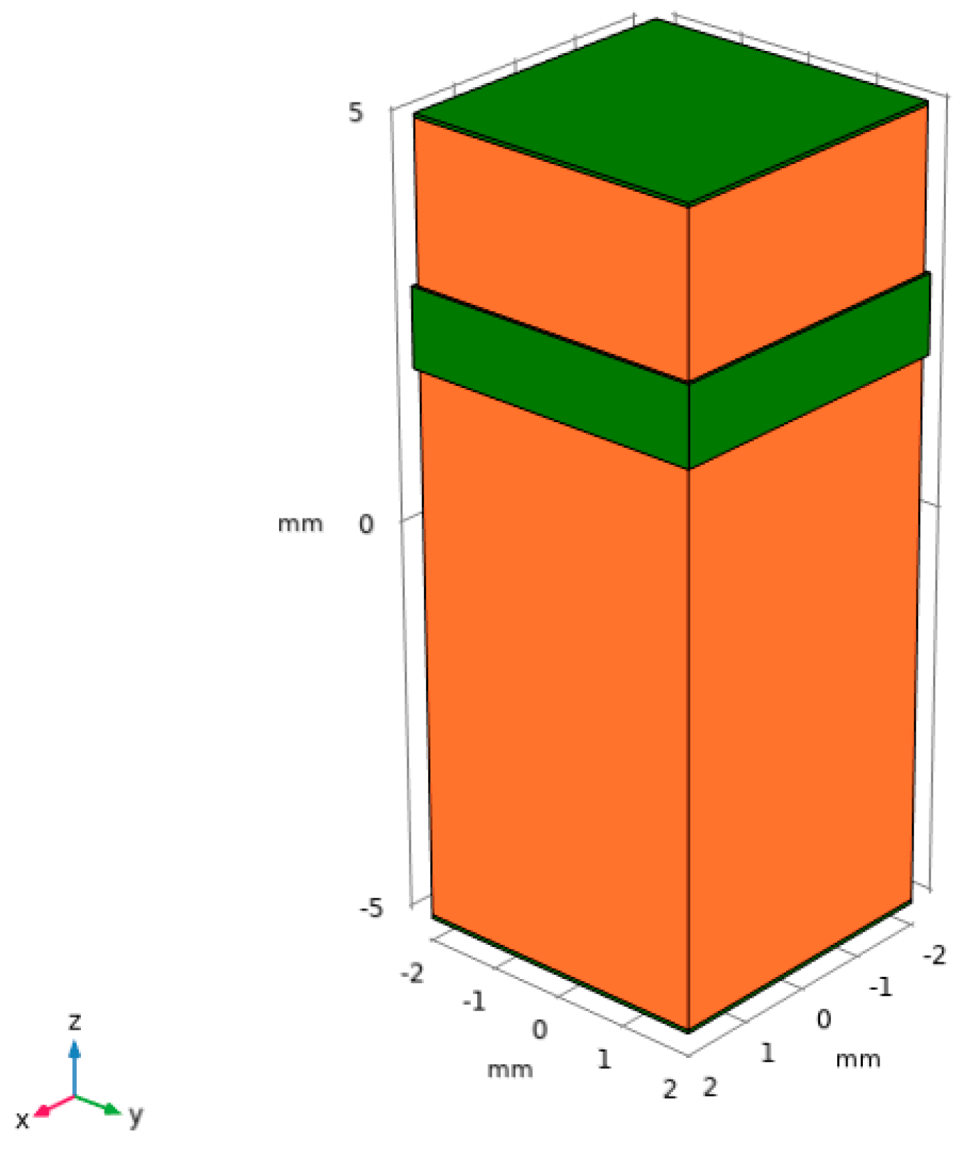
2.3. Modelling of Detectors

The CZT detector was built as a rectangular volume of 4 × 4 × 10 mm3 with an anode at the top and a cathode at the bottom, both materials were set to be Ag, the material of the middle detector part was CZT, and the Frisch grid was in the region close to the anode, and the exact structure is shown in Figure 1. In this study, we mainly consider electron transport with an electron 1000 cm2 V−1s−1. The anode is set to zero potential, and the cathode potential is −600 V. The distribution of the weighting potentials and the electric potentials are obtained by electrostatic field simulation. It is important to note that during mesh generation, attention must be given to the gradient variations in carrier concentration and electric field distribution. Near the electrode contact surface, both the carrier concentration and electric potential exhibit significant changes, requiring mesh refinement in this region to prevent transport calculation errors caused by insufficient resolution. Mesh continuity at the interface must be maintained to avoid potential discontinuities. Additionally, the aspect ratio of the elements should be controlled to prevent distorted elements from affecting solution stability.

3. Results and Discussion

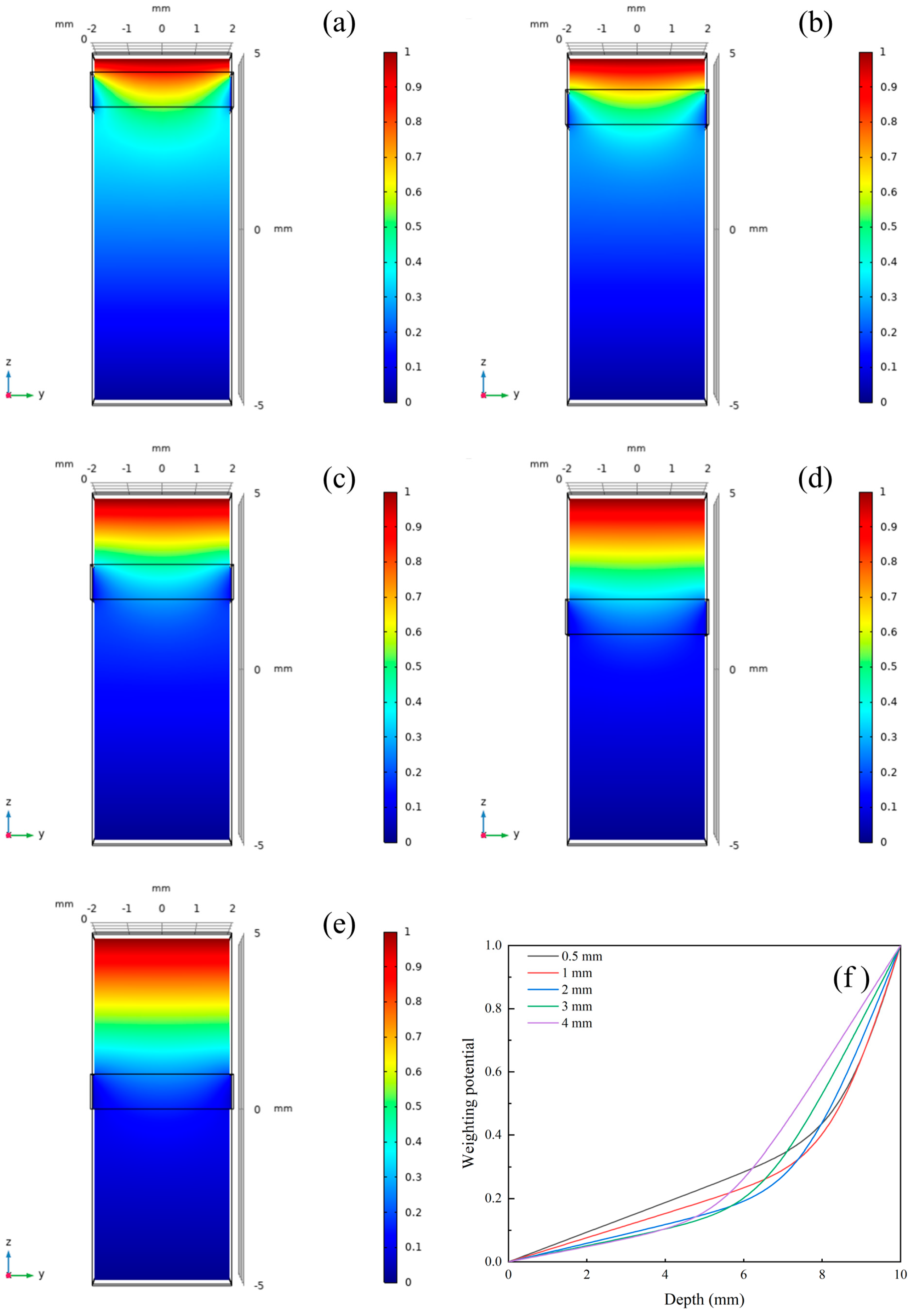
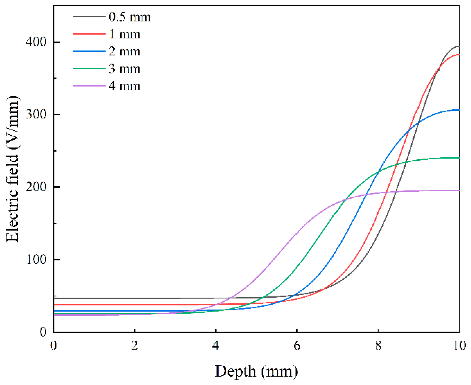
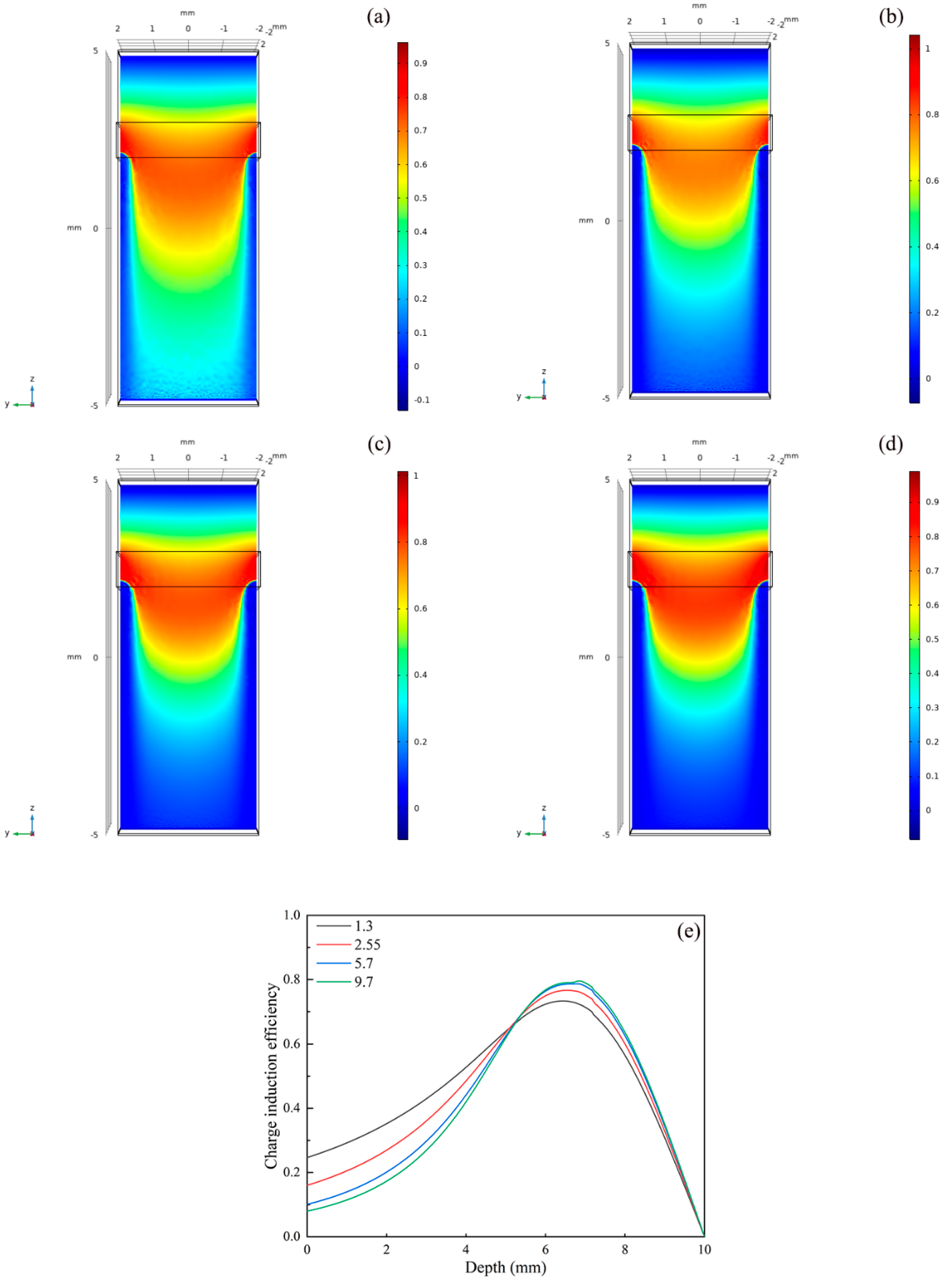
3.1. Effect of Distance Between Frisch Grid and Anode on Detector Performance

In order to understand the effect of the structure of the Frisch grid detector on its performance, we first varied the distance between its grid and anode and then simulated the distributions of the detector’s weight potential, electric field, and charge induction efficiency at different distances. Figure 2 shows the weighting potential of the detector, where Figure 2a–e shows the distribution of the weighting potential at different distances between the grid and the anode, and Figure 2f shows the distribution of the weighting potential on the detector’s centre axis at each distance. From Figure 2a–e, it can be seen that the weight potential in the region between the cathode and the Frisch grid is almost zero, while the weight potential in the region from the Frisch grid to the anode increases rapidly and linearly from 0 to 1. The region between the cathode and the Frisch grid is large in size, and the rays interact with the material in this region, so it is called the interaction region. As can be seen in Figure 2f, as the distance between the grid and the anode decreases, the change in the weighting potential is steeper in the measurement region close to the anode, resulting in a more significant suppression of the induced signals by hole capture, effectively improving the unipolarity of the detector [16].
Figure 3 shows the electric field distribution on the centre axis of the detector at different distances. It can be seen that the electric field varies mainly between the detector grid and the anode, while the electric field between the cathode and the grid is small and uniformly distributed. It can also be observed that as the distance between the grid and the anode decreases, similar to the weighting potential, the electric field varies more steeply between the grid and the anode, which also indicates that the unipolarity of the detector increases as the distance decreases [17,18].
Figure 4 shows a plot of the charge induction efficiency of the detector. Figure 3 shows the distribution of the charge induction efficiency of the detector at different distances, and Figure 4f shows the distribution of the charge induction efficiency on the centre axis. The charge induction efficiency reflects the ability of carriers (electrons) to generate an induced charge at the anode when they migrate to different positions [15]. It can be seen in Figure 4a–e that the locations with higher charge induction efficiency are mainly concentrated near the grid, and the distribution changes significantly with the change in the distance between the grid and the anode. It can be seen in Figure 4b that the distribution of charge induction efficiency on the centre axis changes significantly with distance. As the distance between the grid and the anode decreases, the maximum value of the charge induction efficiency decreases and the position of the highest value moves towards the anode, but in the portion from the grid to the cathode, the charge induction efficiency is more evenly distributed, and its value varies more smoothly from the cathode to the grid, with a higher average value. For the detector, a more balanced charge induction efficiency distribution results in a larger detector action volume, reducing the detector dead zone area and improving detector performance [18].
From the simulation results, it can be found that in the Frisch grid detector, decreasing the distance between the gate and the anode can effectively improve the unipolarity of the detector, reduce the effect of holes on the induction signal, and lead to a more even distribution of charge induction efficiency, and it seems that a lower distance between the gate and the anode leads to better performance of the detector. However, too small a distance between the grid and the anode may create problems; in general, the smaller the distance between the grid and the anode, the more responsive the detector is to the particles, the higher the signal strength, and the better the resolution is likely to be [19]. But, if the distance is too small, it may increase the noise level of the detector and affect the clarity of the signal [20,21]. And a proper distance from the grid to the anode can help avoid discharges and breakdowns. If the distance is too small, it can increase the voltage gradient between the grid and the anode, leading to discharge or breakdown, which can damage the detector and reduce its performance [22]. The difference between the weighting potential and charge induction efficiency distribution of the detectors with distances of 0.5 mm and 1 mm, respectively, in the simulation results is very small, and the charge induction efficiency distribution of the detector with a distance of 1 mm is not as average as that with a distance of 0.5 mm, but the magnitude is basically able to reach more than 0.35. Considering the possible problems mentioned in the previous section, the practical application of the detector with a distance of 1 mm may be better than that of the detector with a distance of 0.5 mm [22,23].

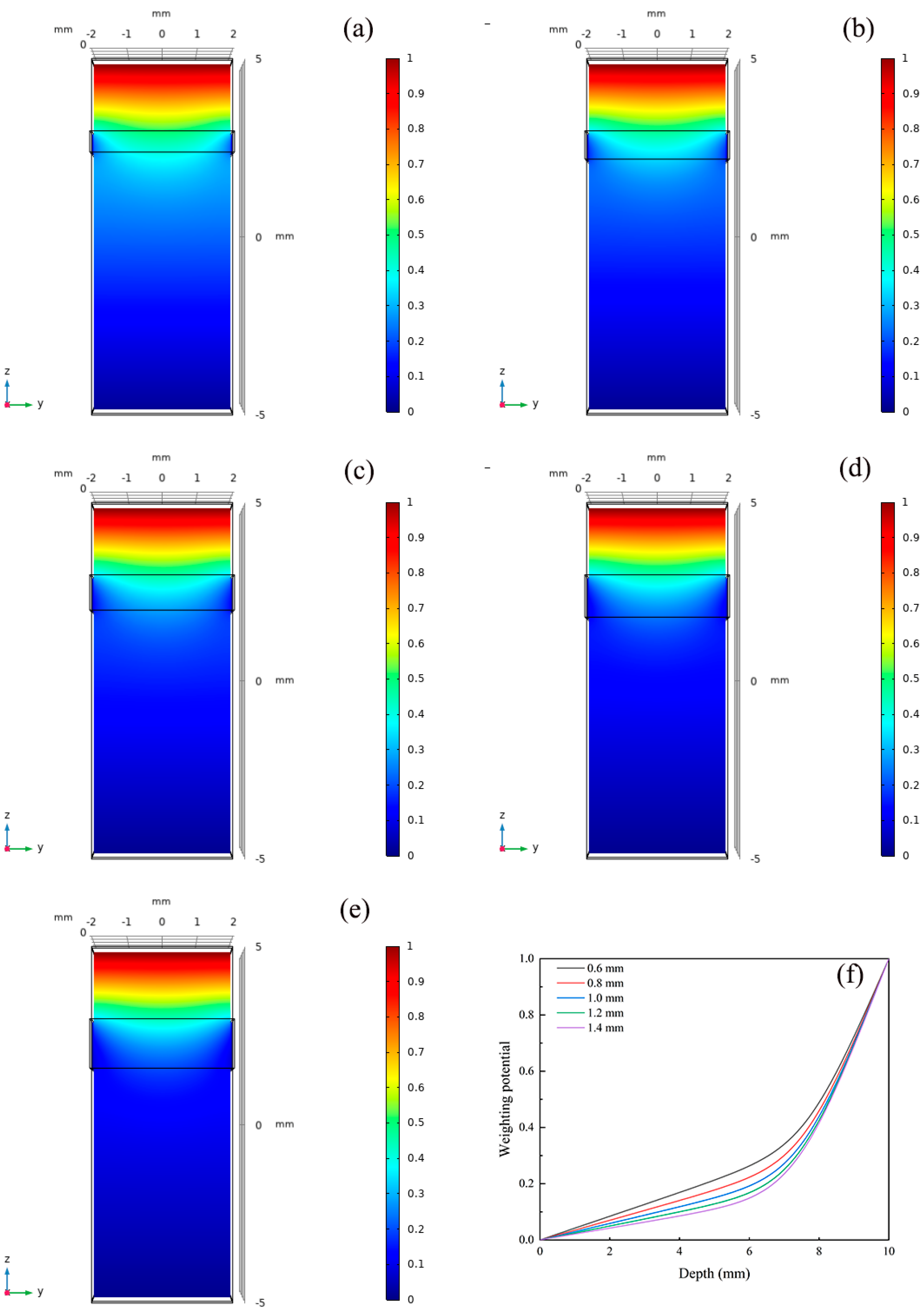
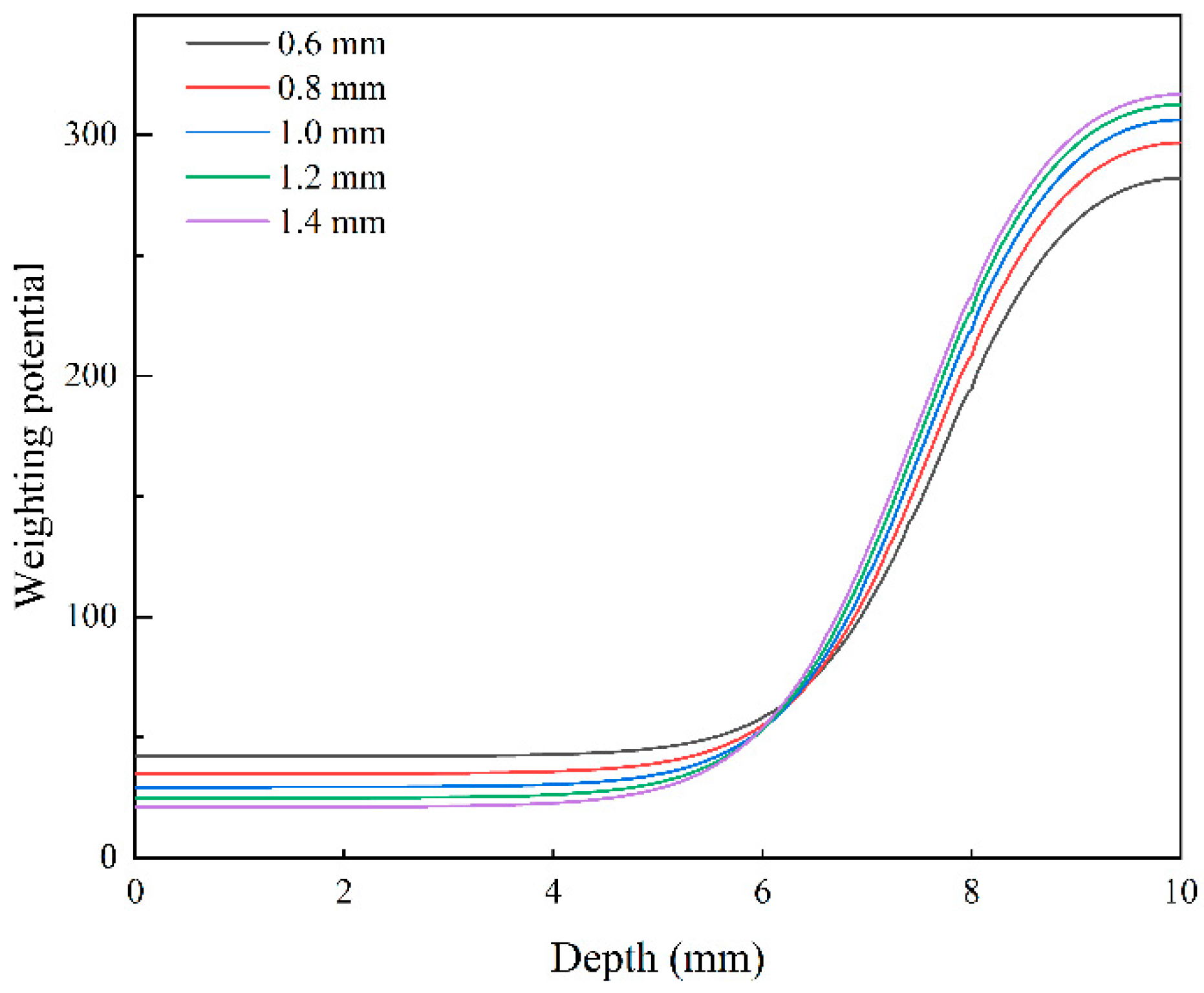
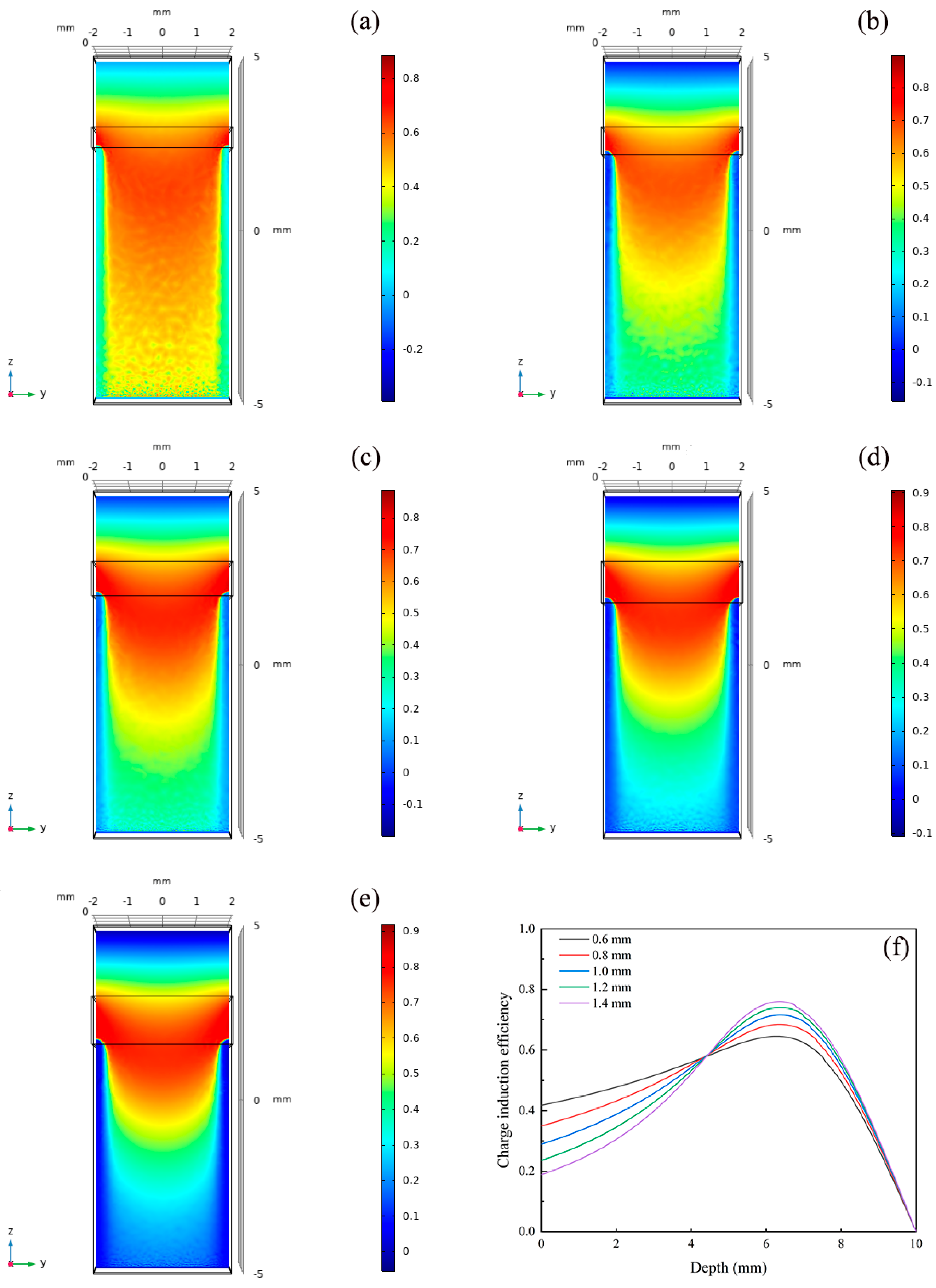
3.2. Effect of Frisch Grid Area on Detector Performance

Figure 5 shows the weight potential of the CZT detector with different grid areas, where Figure 5a–e shows the weight potential distribution of the detector with different areas, and Figure 5f shows the weight potential distribution on the detector’s central axis. We varied the area of the grid by changing its height. The weighting potential, electric field and charge induction efficiency are simulated for five cases with heights of 0.6 mm, 0.8 mm, 1 mm, 1.2 mm and 1.4 mm. From Figure 5a–e, it can be seen that as the area of the grid increases, the blue colour between the grid and cathode gradually deepens, which indicates that the change in the weighting potential at the location between the grid and cathode decreases, and it can also be seen that the change in the colour representing the distribution of the weighting potential is gradually concentrated between the grid and anode, with the red region gradually being compressed to the vicinity of the anode. These phenomena can reflect that the unipolarity of the detector increases significantly with the increase in the grid area. It is also clear in Figure 5f that the change in the weight potential between the cathode and the grid is smoother, and the change in the weight potential between the anode and the grid is more intense as the gate area increases [19].
Figure 6 shows the distribution of the electric field on the centre axis of the detector for different grid areas. It is clear from the figure that the electric field strength is showing an increasing trend from the cathode to the anode of the detector, and in the case of a large grid area, the electric field strength is smaller and rises more slowly between the cathode and the grid. The electric field strength from the anode to the grid is bigger and rises faster. This demonstrates a significant improvement in the unipolarity of the detector as the area of the grid increases [24].
Figure 7 shows the charge induction efficiency of the detector for different grid areas. Figure 7a–e shows the distribution of charge induction efficiency inside the detector for different areas, and Figure 7f shows the distribution of charge induction efficiency on the centre axis of the detector for different areas. From Figure 7a–e, it can be seen that as the area of the Frisch grid increases, the variation in the charge induction efficiency inside the detector gradually concentrates towards the gate position, with the charge induction efficiency near the cathode gradually decreasing and that near the grid gradually increasing. Whereas it can be seen in Figure 7f that the increase in the grid area results in a very significant increase in the maximum value of the charge induction efficiency, with the extreme value of the charge induction efficiency increasing from 0.636 to 0.755 during the increase in the gate height from 0.6 to 1.4 mm. This is due to the charge diffusion of the generated charge carriers as they drift over a larger area before reaching the collection electrodes. The Frisch grid covers a larger portion of the crystal volume and effectively confines the charge carriers to a defined region, thereby minimising charge spreading and improving charge induction efficiency [25]. However, it should be noted that the increase in the grid area makes the distribution of the charge induction efficiency more uneven, the charge induction efficiency near the cathode decreases, and the change in the charge induction efficiency between the grid and the anode is more intense. Previous studies have shown that as the gate area increases, the distribution of the weighting potential becomes more concentrated, and the device’s unipolarity improves. Based on the formula from earlier research, we can observe that the charge induction efficiency distribution is closely related to the weighting potential distribution. As the gate area increases, the uniformity of the weighting potential distribution decreases, and the weighting potential between the cathode and the gate decreases, leading to a corresponding decrease in charge induction efficiency. The rate of increase in weighting potential between the gate and anode becomes steeper, causing more drastic changes in charge induction efficiency.
From the simulation results we are able to find that the increase in the grid area significantly improves the unipolarity of the detector and reduces the effect of holes on the induced charge, which contributes to the improvement of the detector resolution, and the increase in the gate area also contributes to the increase in the charge induction efficiency [17]. However, a large gate area results in an uneven distribution of charge induction efficiency, which may increase the dead area of the detector and thus affect the detector performance, and an excessively large Frisch grid area may introduce additional capacitance, which reduces the energy resolution and increases the electronic noise [26,27].

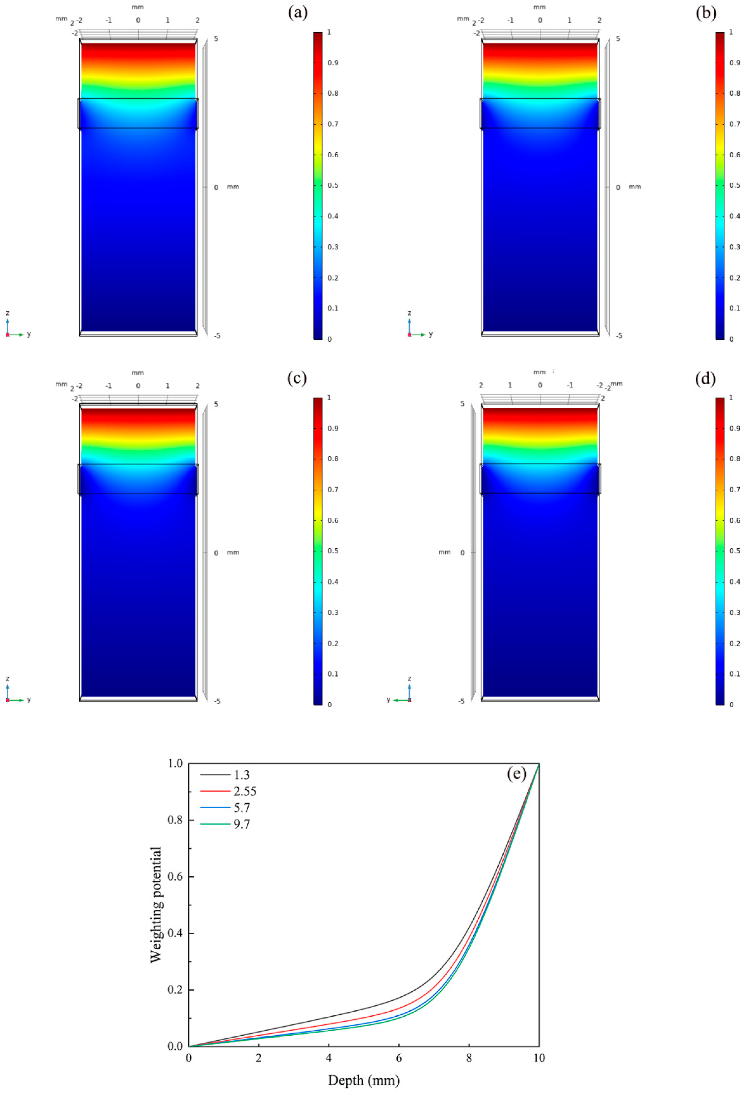
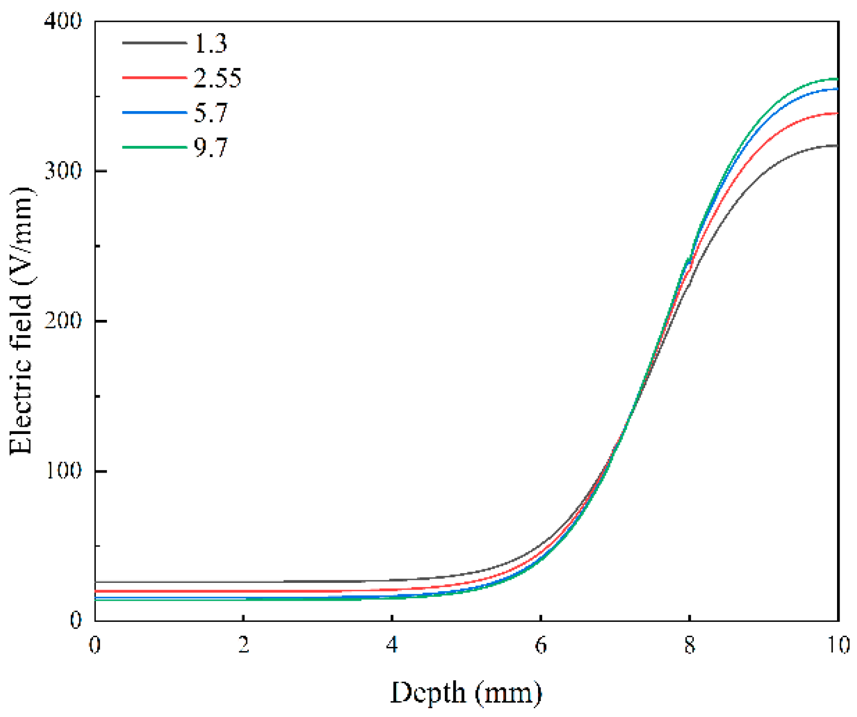
3.3. Effect of Relative Permittivity of Frisch Grid Material on Detector Performance

In addition to exploring the effect of the physical structure of the Frisch grids on the detector, the effect of Frisch grids prepared from different materials on the detector was also modelled, where we varied the relative permittivity to represent the differences in the Frisch grid materials. The materials and relative permittivities chosen were Au: 1.3, Ag: 2.55, Cu: 5.7 and Al: 9.7.
Figure 8 shows the weighting potentials of the permittivity CZT detectors with different grid materials, where Figure 8a–d shows the distribution of the weighting potentials of the detectors with different areas, and Figure 8e shows the distribution of the weighting potentials on the centre axis of the detectors. From Figure 8a–d, it can be seen that the variation in the weighted potential at the position between the grid and the cathode decreases slightly as the permittivity increases, and the colour change representing the distribution of the weighted potential gradually concentrates between the grid and the anode, and the red region is gradually compressed to the vicinity of the anode. These phenomena can reflect that the unipolarity of the detector increases with the increase in permittivity. It is also clear from Figure 8e that the change in weighted potential between the cathode and the grid is smoother, and the change in weighted potential between the anode and the grid is stronger as the permittivity increases [18].
Figure 9 shows the electric field distribution on the centre axis of the detector for different relative permittivities of the grid material. It is clear from the figure that the electric field strength tends to rise from the cathode to the anode of the detector. Similarly to the weighted potential distribution, the electric field strength between the cathode and the grid is smaller and rises more slowly in the case of permittivity. The electric field strength from the anode to the grid is greater and rises faster. This suggests that also with increasing permittivity, the unipolarity of the detector improves [28].
Figure 10 shows the charge induction efficiency of the detector with different permittivity of the grid material. Figure 10a–d shows the distribution of charge induction efficiency inside the detector at different regions, and Figure 10e shows the distribution of charge induction efficiency on the centre axis of the detector at different regions. From Figure 10a–d, it can be seen that the variation in the charge induction efficiency inside the detector is slightly concentrated towards the grid position as the permittivity increases, with a gradual decrease in the charge induction efficiency near the cathode and a gradual increase in the charge induction efficiency near the grid. And from Figure 10e, it can be seen that the increase in the permittivity leads to the increase in the maximum value of the charge induction efficiency, and the extreme value of the charge induction efficiency increases from 0.730 to 0.795. However, it should be noted that the increase in the grid area leads to a more inhomogeneous distribution of the charge induction efficiency, with a decrease in the charge induction efficiency near the cathode and a more drastic change in the charge induction efficiency between the grid and the cathode.
From the simulation results, it can be found that the selection of materials with high relative permittivity can improve the unipolarity of the detector and reduce the effect of holes on the induced charge, thus improving the resolution of the detector, as well as contributing to the charge induction efficiency. However, high dielectric constant materials may bring more electronic noise due to the increase in capacitance, resulting in a lower signal-to-noise ratio and thus lower energy resolution [29].

4. Discussion

In this paper, finite element simulation software was used to simulate the performance of the Frisch grid CZT detector, and the weight potential, electric field and charge induction efficiency distributions of the detector were simulated with different physical structures of Frisch grids and preparation materials, and the optimisation ideas on the structure and materials of the Frisch grid CZT detector were proposed. The simulation results show that reducing the distance between the Frisch grid and the anode helps to improve the unipolarity of the detector so that the charge induction efficiency distribution is also more uniform. However, it is still important to note that lower grid-to-anode spacing decreases the maximum value of charge induction efficiency and that a lower distance increases the voltage gradient between the grid and anode, leading to discharge or breakdown. Increasing the Frisch grid area is also a good way to increase the unipolarity of the detector and increase the maximum value of the charge induction efficiency, but at the same time, a large grid area can reduce the uniformity of the charge induction efficiency distribution and introduce additional capacitance increasing noise. Selection of materials with large relative permittivity can also significantly improve the unipolarity of the detector, but similar to increasing the Frisch gate area, a large relative permittivity will increase the maximum value of the charge induction efficiency and, at the same time, reduce the uniformity of the distribution of the charge induction efficiency, and a high permittivity may likewise lead to an increase in capacitance and noise, lowering the detector signal-to-noise ratio and affecting the detector resolution. From the simulation results, the optimisation of the performance of the Frisch grid detector is mainly based on minimising the distance between the gate and anode within a reasonable interval, increasing the area of the Frisch grid and selecting a material with a high relative permittivity for the preparation of the Frisch grid.

Author Contributions

Conceptualization, M.C.; methodology, M.C.; software, W.H.; validation, Z.X.; formal analysis, Z.Z.; investigation, L.W.; resources, L.W.; data curation, Z.X.; writing—original draft preparation, Z.Z.; writing—review and editing, J.H.; visualization, Y.L.; supervision, J.H.; project administration, M.C.; funding acquisition, L.W. All authors have read and agreed to the published version of the manuscript.

Funding

This research was funded by the State Key Laboratory of Infrared Physics (Grant no. SITP-NLIST-YB-2023-17).

Data Availability Statement

Data in this manuscript is unavailable due to privacy reason.

Acknowledgments

This paper is supported by the National Key R&D Program of China (No. 2023YFA1608703).

Conflicts of Interest

The authors declare no conflicts of interest.

References

  1. Sordo, S.D.; Abbene, L.; Caroli, E.; Mancini, A.M.; Zappettini, A.; Ubertini, P. Progress in the development of CdTe and CdZnTe semiconductor radiation detectors for astrophysical and medical applications. Sensors 2009, 9, 3491–3526. [Google Scholar] [CrossRef] [PubMed]
  2. Pennicard, D.; Pirard, B.; Tolbanov, O.; Iniewski, K. Semiconductor materials for X-ray detectors. MRS Bull. 2017, 42, 445–450. [Google Scholar] [CrossRef]
  3. Kasap, S.O.; Willoughby, A. Mercury Cadmium Telluride: Growth, Properties and Applications; John Wiley & Sons: Hoboken, NJ, USA, 2011. [Google Scholar]
  4. Eisen, Y.; Shor, A. CdTe and CdZnTe materials for room-temperature X-ray and gamma ray detectors. J. Cryst. Growth 1998, 184, 1302–1312. [Google Scholar] [CrossRef]
  5. Myronakis, M.E.; Zvelebil, M.; Darambara, D.G. Pixelated CdZnTe for imaging in medicine: Overall performance assessment using an advanced computational modeling framework. In Proceedings of the 2012 IEEE Nuclear Science Symposium and Medical Imaging Conference Record, Anaheim, CA, USA, 29 October–3 November 2012; IEEE: New York, NY, USA, 2012; pp. 4276–4277. [Google Scholar]
  6. Iniewski, K. CZT detector technology for medical imaging. J. Instrum. 2014, 9, C11001. [Google Scholar] [CrossRef]
  7. Roy, U.N.; Camarda, G.S.; Cui, Y.; James, R.B. High-resolution virtual Frisch grid gamma-ray detectors based on as-grown CdZnTeSe with reduced defects. Appl. Phys. Lett. 2019, 114, 232107. [Google Scholar] [CrossRef]
  8. Bolotnikov, A.E.; Camarda, G.S.; Carini, G.A.; Wright, G.W.; McGregor, D.S.; McNeil, W.; James, R.B. New results from performance studies of Frisch-grid CdZnTe detectors. In Hard X-Ray and Gamma-Ray Detector Physics VI; SPIE: Bellingham, WA, USA, 2004; pp. 33–45. [Google Scholar]
  9. Limousin, O. New trends in CdTe and CdZnTe detectors for X-and gamma-ray applications. Nucl. Instrum. Methods Phys. Res. Sect. A Accel. Spectrometers Detect. Assoc. Equip. 2003, 504, 24–37. [Google Scholar] [CrossRef]
  10. Sze, S.M. Semiconductor Devices: Physics and Technology; John Wiley & Sons: Hoboken, NJ, USA, 2008. [Google Scholar]
  11. Prettyman, T. Method for mapping charge pulses in semiconductor radiation detectors. Nucl. Instrum. Methods Phys. Res. Sect. A Accel. Spectrometers Detect. Assoc. Equip. 1999, 422, 232–237. [Google Scholar] [CrossRef]
  12. Makeev, A.; McGrath, J.; Clajus, M.; Snyder, S.; Glick, S.J. Achieving sub-pixel resolution using CZT-based photon counting detectors for dedicated breast CT. In Medical Imaging 2013: Physics of Medical Imaging; SPIE: Bellingham, WA, USA, 2013; pp. 211–218. [Google Scholar]
  13. He, Z. Review of the Shockley–Ramo theorem and its application in semiconductor gamma-ray detectors. Nucl. Instrum. Methods Phys. Res. Sect. A Accel. Spectrometers Detect. Assoc. Equip. 2001, 463, 250–267. [Google Scholar] [CrossRef]
  14. Makeev, A.; Rodrigues, M.; Wang, G.-C.; Glick, S.J. Modeling CZT/CdTe X-ray photon-counting detectors. In Medical Imaging 2015: Physics of Medical Imaging; SPIE: Bellingham, WA, USA, 2015. [Google Scholar]
  15. Myronakis, M.E.; Darambara, D.G. Monte Carlo investigation of charge-transport effects on energy resolution and detection efficiency of pixelated CZT detectors for SPECT/PET applications. Med. Phys. 2011, 38, 455–467. [Google Scholar] [CrossRef]
  16. McGregor, D.; He, Z.; Seifert, H.; Rojeski, R.; Wehe, D. CdZnTe semiconductor parallel strip Frisch grid radiation detectors. IEEE Trans. Nucl. Sci. 1998, 45, 443–449. [Google Scholar] [CrossRef]
  17. Luke, P. Unipolar charge sensing with coplanar electrodes-application to semiconductor detectors. IEEE Trans. Nucl. Sci. 1995, 42, 207–213. [Google Scholar] [CrossRef]
  18. Nakhostin, M. Signal Processing for Radiation Detectors; John Wiley & Sons: Hoboken, NJ, USA, 2017. [Google Scholar]
  19. Charpak, G.; Sauli, F. High-resolution electronic particle detectors. In Experimental Techniques in High-Energy Nuclear and Particle Physics; Ferbel, T., Ed.; World Scientific Publishing Co., Pte. Ltd: Singapore, 1991. [Google Scholar]
  20. Siewerdsen, J.H.; Antonuk, L.E.; El-Mohri, Y.; Yorkston, J.; Huang, W.; Cunningham, I.A. Signal, noise power spectrum, and detective quantum efficiency of indirect-detection flat-panel imagers for diagnostic radiology. Med. Phys. 1998, 25, 614–628. [Google Scholar] [CrossRef] [PubMed]
  21. Radeka, V. Low-noise techniques in Detectors. Annu. Rev. Nucl. Part. Sci. 1988, 38, 217–277. [Google Scholar] [CrossRef]
  22. Garrett, H.B.; Whittlesey, A.C. Guide to Mitigating Spacecraft Charging Effects; John Wiley & Sons: Hoboken, NJ, USA, 2012. [Google Scholar]
  23. Al-Adili, A.; Hambsch, F.J.; Bencardino, R.; Pomp, S.; Oberstedt, S.; Zeynalov, S. On the Frisch–Grid signal in ionization chambers. Nucl. Instrum. Methods Phys. Res. Sect. A Accel. Spectrometers Detect. Assoc. Equip. 2012, 671, 103–107. [Google Scholar] [CrossRef]
  24. Hötzl, H.; Winkler, R. Experiences with large-area frisch grid chambers in low-level alpha spectrometry. Nucl. Instrum. Methods Phys. Res. 1984, 223, 290–294. [Google Scholar] [CrossRef]
  25. Kolstein, M.; Ariño, G.; Chmeissani, M.; De Lorenzo, G. Simulation of charge transport in pixelated CdTe. J. Instrum. 2014, 9, C12027. [Google Scholar] [CrossRef] [PubMed]
  26. Polack, J.; Hirt, M.; Sturgess, J.; Sferrazza, N.; Bolotnikov, A.; Babalola, S.; Camarda, G.; Cui, Y.; Egarievwe, S.; Fochuk, P. Variation of electric shielding on virtual Frisch-grid detectors. Nucl. Instrum. Methods Phys. Res. Sect. A Accel. Spectrometers Detect. Assoc. Equip. 2010, 621, 424–430. [Google Scholar] [CrossRef]
  27. Bolotnikov, A.E.; Ackley, K.; Camarda, G.S.; Cherches, C.; Cui, Y.; De Geronimo, G.; Fried, J.; Hodges, D.; Hossain, A.; Lee, W.; et al. An array of virtual Frisch-grid CdZnTe detectors and a front-end application-specific integrated circuit for large-area position-sensitive gamma-ray cameras. Rev. Sci. Instrum. 2015, 86, 073114. [Google Scholar] [CrossRef] [PubMed]
  28. Cui, Y.; Bolotnikov, A.; Camarda, G.; Hossain, A.; Yang, G.; James, R. CZT virtual Frisch-grid detector: Principles and applications. In Proceedings of the 2009 IEEE Long Island Systems, Applications and Technology Conference, Farmingdale, NY, USA, 1 May 2009; IEEE: New York, NY, USA, 2009; pp. 1–5. [Google Scholar]
  29. Uram, J.D.; Ke, K.; Mayer, M. Noise and bandwidth of current recordings from submicrometer pores and nanopores. ACS Nano 2008, 2, 857–872. [Google Scholar] [CrossRef] [PubMed]
Figure 1. Schematic diagram of the structure of the Frisch gird detector.
Crystals 15 00361 g001
Figure 2. Detector weight potential distribution for different grid anode distances: (a) 0.5 mm, (b) 1 mm, (c) 2 mm, (d) 3 mm, (e) 4 mm, (f) variation in the weighting potential of the detector mid-axis with depth for different grid anode distances.
Crystals 15 00361 g002
Figure 3. Variation in the electric field with depth at the detector mid-axis for different grid anode distances.
Crystals 15 00361 g003
Figure 4. Charge induction efficiency distribution of detectors with different grid anode distances: (a) 0.5 mm, (b) 1 mm, (c) 2 mm, (d) 3 mm, (e) 4 mm, (f) variation in the charge induction efficiency of the detector mid-axis with depth for different grid anode distances.
Crystals 15 00361 g004
Figure 5. Weight potential distribution of detectors with different grid heights: (a) 0.6 mm, (b) 0.8 mm, (c) 1/0 mm, (d) 1.2 mm, (e) 1.4 mm, (f) variation in the weighting potential of the detector mid-axis with depth for different gird heights.
Crystals 15 00361 g005
Figure 6. Variation in the electric field of the detector mid-axis with depth for different grid heights.
Crystals 15 00361 g006
Figure 7. Charge induction efficiency distribution of detectors with different grid heights: (a) 0.6 mm, (b) 0.8 mm, (c) 1.0 mm, (d) 1.2 mm, (e) 1.4 mm, (f) variation in the charge induction efficiency of the detector mid-axis with depth for different grid heights.
Crystals 15 00361 g007
Figure 8. Weight potential distribution of detectors with different relative permittivities of gird: (a) 1.3, (b) 2.55, (c) 5.7, (d) 9.7, (e) variation in the weighting potential of the detector mid-axis with depth for different grid relative permittivities.
Crystals 15 00361 g008
Figure 9. Variation in the electric field of the detector mid-axis with depth for different grid relative permittivities.
Crystals 15 00361 g009
Figure 10. Charge induction efficiency distribution of detectors with different relative permittivities of grid: (a) 1.3, (b) 2.55, (c) 5.7, (d) 9.7, (e) variation in the charge induction efficiency of the detector mid-axis with depth for different grid relative permittivities.
Crystals 15 00361 g010
Disclaimer/Publisher’s Note: The statements, opinions and data contained in all publications are solely those of the individual author(s) and contributor(s) and not of MDPI and/or the editor(s). MDPI and/or the editor(s) disclaim responsibility for any injury to people or property resulting from any ideas, methods, instructions or products referred to in the content.

