
Research on the Fabrication of X-Cut Near Stoichiometric Lithium Niobate Wafers

 ,
,
Abstract
1. Introduction
2. Experiment
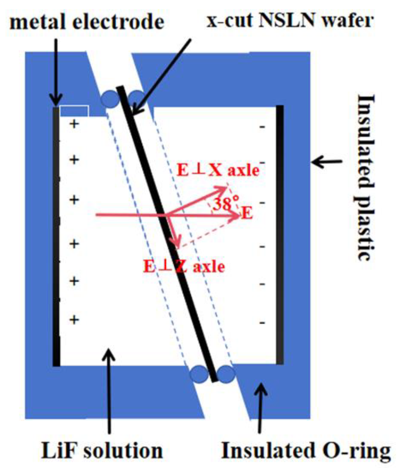
2.1. Diffused Polycrystalline
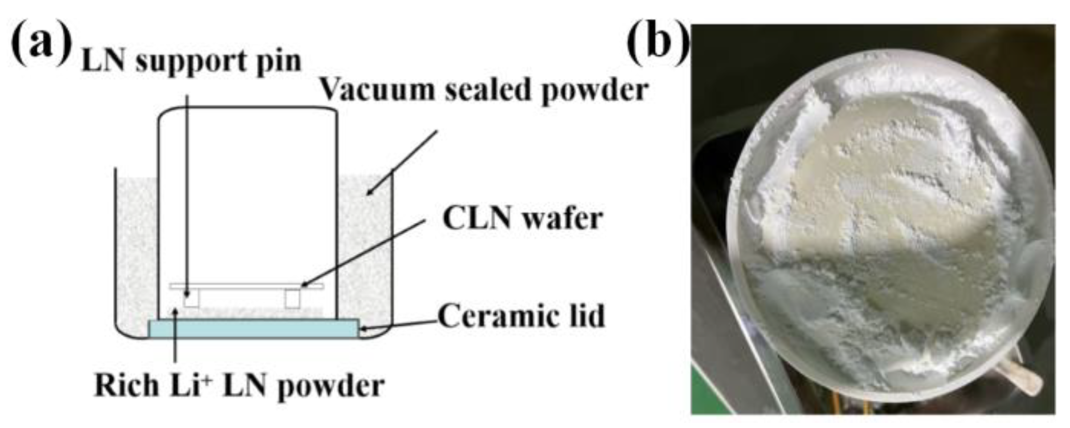
2.2. Preparation of NSLN
2.3. Characterization
3. Results and Discussion
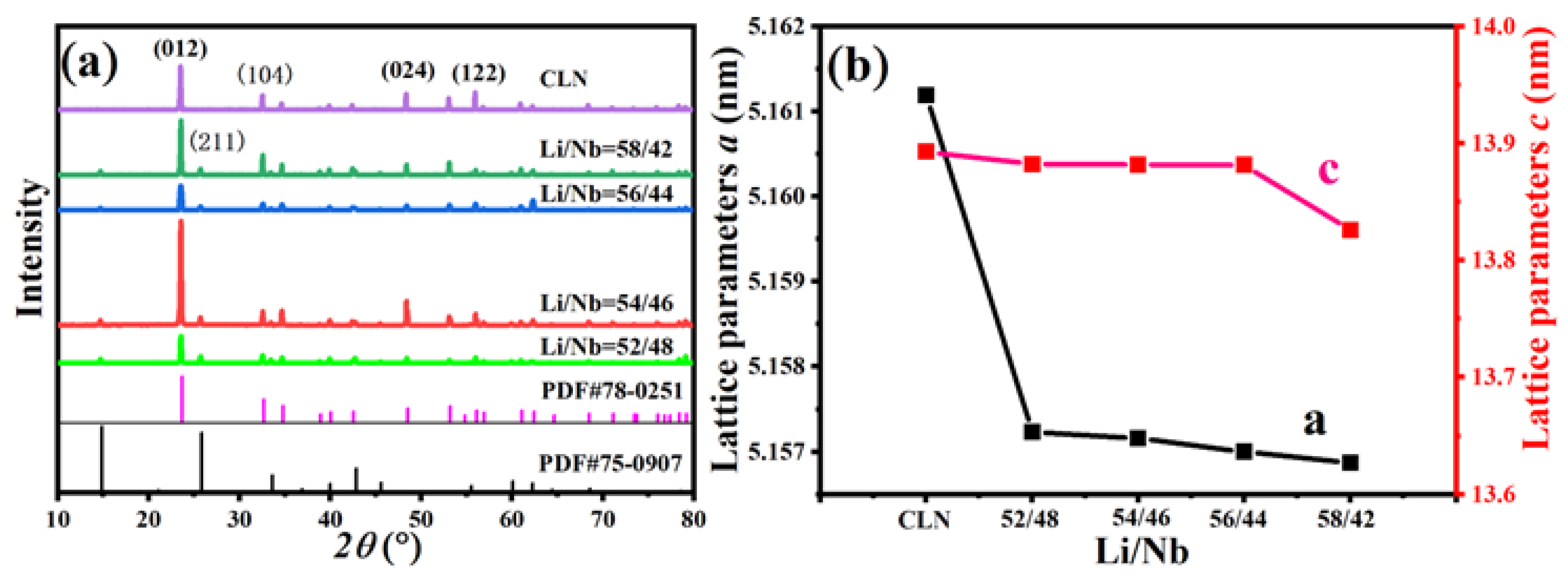
3.1. XRD Characterization of Diffusion Materials
3.2. Discussion on Wafer Diffusion Process
3.3. Micro Domain Elimination Process and Single Domain Characterization

3.4. Curie Temperature Test

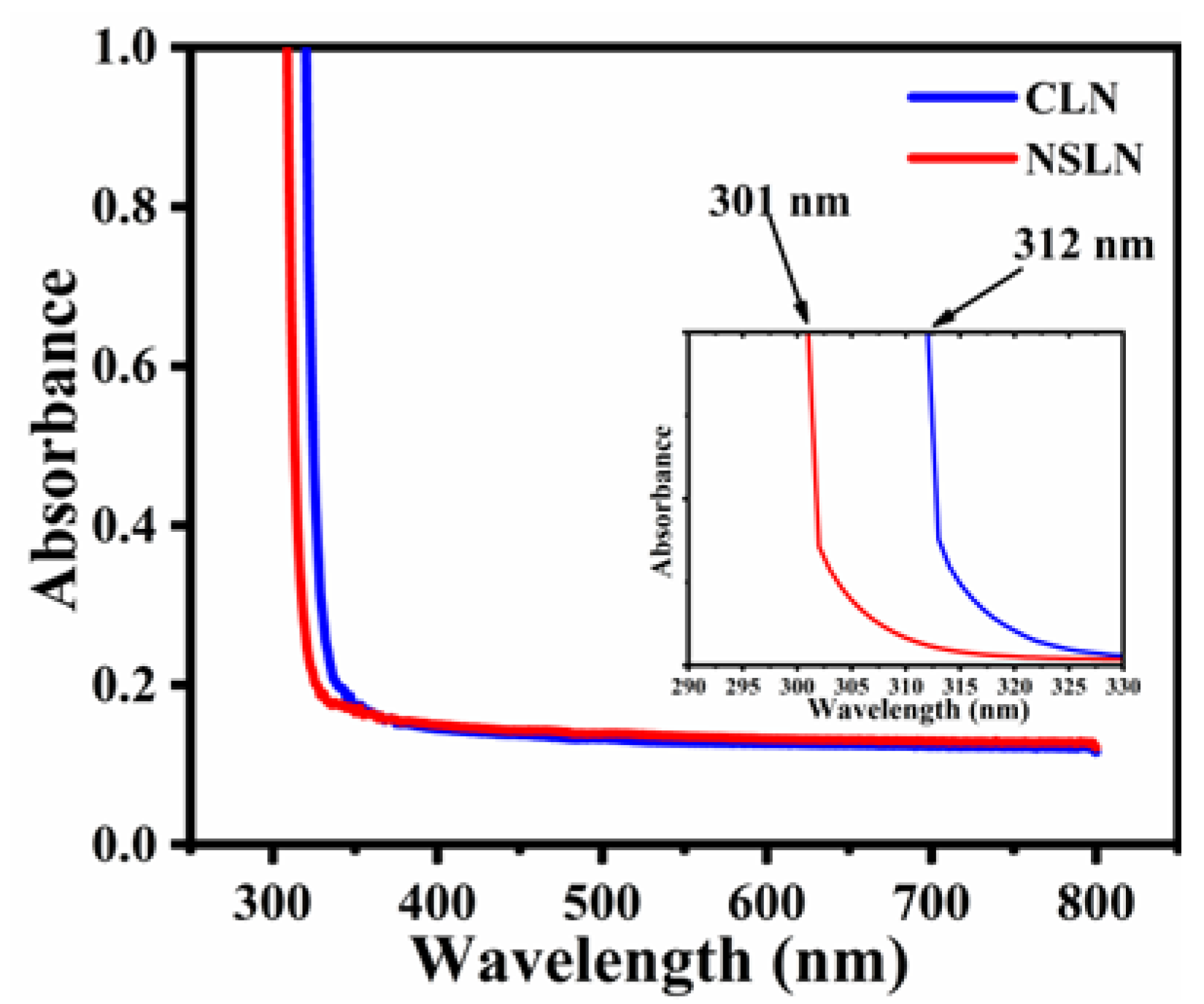
3.5. UV Absorption Spectrum
3.6. Refractive Index
4. Summary
Author Contributions
Funding
Data Availability Statement
Acknowledgments
Conflicts of Interest
References
- Lyu, J.B.; Zhu, T.; Zhou, Y.; Chen, Z.M.; Pi, Y.Z.; Liu, Z.T.; Xu, X.C.; Xu, K.; Ma, X.; Wang, L.; et al. Inverse design for material anisotropy and its application for a compact X-cut TFLN on-chip wavelength demultiplexer. OES 2023, 2, 230038–230041. [Google Scholar] [CrossRef]
- Cheng, W.; Mian, Z.; Xi, C.; Bertrand, M.; Shams-Ansari, A.; Chandrasekhar, S.; Winzer, P.; Loncar, M. Integrated lithium niobate electro-optic modulators operating at CMOS-compatible voltages. Nature 2018, 562, 101–104. [Google Scholar] [CrossRef]
- Zhu, D.; Shao, L.B.; Yu, M.J.; Cheng, R.; Desiaov, C.J.; Xu, Y.W.; Holzgrafe, J.; Ghosh, S.; Shams-Ansari, A.; Puma, E.; et al. Integrated photonics on thin-film lithium niobate. Adv. Opt. Photonics 2021, 13, 242–352. [Google Scholar] [CrossRef]
- Lengyel, K.; Péter, Á.; Kovács, L.; Corradi, G.; Pálfalvi, L.; Hebling, J.; Unferdorben, M.; Dravecz, G.; Hajdara, I.; Szaller, Z.; et al. Growth, defect structure, and THz application of stoichiometric lithium niobate. Appl. Phys. Rev. 2015, 2, 040601. [Google Scholar] [CrossRef]
- Mercante, A.J.; Shi, S.; Yao, P.; Xie, L.L.; Weikle, R.; Prather, D. Thin film lithium niobate electro-optic modulator with terahertz operating bandwidth. Opt. Express 2018, 26, 14810. [Google Scholar] [CrossRef]
- Rao, A.; Patil, A.; Rabiei, P.; Honardoost, A.; DeSalvo, R.; Paolella, A.; Fathpour, S. High-performance and linear thin-film lithium niobate Mach–Zehnder modulators on silicon up to 50 GHz. Opt. Lett. 2016, 41, 5700–5703. [Google Scholar] [CrossRef]
- Toro, J.A.; Serrano, M.D.; Cabañes, A.G.; Cabrera, J.M. Accurate interferometric measurement of electro-optic coefficients: Application to quasi-stoichiometric LiNbO3. Opt. Commun. 1998, 154, 23–27. [Google Scholar] [CrossRef]
- Iyi, N.; Kitamura, K.; Izumi, F.; Yamamoto, J.K.; Hayashi, T.; Asano, H.; Kimura, S. Comparative study of defect structures in lithium niobate with different compositions. J. Solid State Chem. 1992, 101, 340–352. [Google Scholar] [CrossRef]
- Kong, Y.; Bo, F.; Wang, W.; Zheng, D.; Liu, H.; Zhang, G.; Rupp, R.; Xu, J. Recent progress in lithium niobate: Optical damage, defect simulation, and on-chip devices. Adv. Materi. 2020, 32, 1806452. [Google Scholar] [CrossRef]
- Fujiwara, T.; Takahashi, M.; Ohama, M.; Ikushima, A.J.; Furukawa, Y.; Kitamura, K. Comparison of electro-optic effect between stoichiometric and congruent LiNbO3. Electro. Lett. 1999, 35, 499–501. [Google Scholar] [CrossRef]
- Xue, D.; Zhang, S. The effect of stoichiometry on nonlinear optical properties of LiNbO3. J. Phys. Condens. Matter 1997, 9, 7515. [Google Scholar] [CrossRef]
- Klein, R.S.; Kugel, G.E.; Maillard, A.; Plgar, K.; Peter, A. Absolute non-linear optical coefficients of LiNbO3 for near stoichiometric crystal compositions. Opt. Mater. 2003, 22, 171–174. [Google Scholar] [CrossRef]
- Xiong, X.; Cao, Q.-T.; Xiao, Y.-F. Thin-film lithium niobate photonic integrated devices: Advances and oppotunities. Acta Phys. Sin. 2023, 72, 234201. [Google Scholar] [CrossRef]
- Ganesamoorthy, S.; Nakamura, M.; Takekawa, S.; Kumaragurubaran, S.; Terabe, K.; Kitamura, K. A comparative study on the domain switching characteristics of near stoichiometric lithium niobate and lithium tantalate single crystals. Mater. Sci. Eng. B 2005, 120, 125–129. [Google Scholar] [CrossRef]
- Sidorov, N.V.; Antonycheva, E.A.; Syuĭ, A.V.; Palatnikov, M.N. Photorefractive properties of stoichiometric lithium niobate single crystals. Crystallogr. Rep. 2010, 55, 1019–1024. [Google Scholar] [CrossRef]
- Xiao, X.; Si, J.; Liang, S.; Xu, Q.; Zhang, H.; Ma, L.; Yang, C.; Zhang, X. Preparation, Properties, and Applications of Near Stoichiometric Lithium Tantalate Crystals. Crystals 2023, 13, 1031. [Google Scholar] [CrossRef]
- Furukawa, Y.; Kitamura, K.; Ji, Y.; Zgonik, M.; Medrano, C.; Günter, P. Photorefractive properties of iron-doped stoichiometric lithium niobate. Opt. Lett. 1997, 22, 501–503. [Google Scholar] [CrossRef]
- Elkus, B.S.; Abdelsalam, K.; Rao, A.; Velev, V.; Fathpour, S.; Kumar, P.; Kanter, S. Generation of broadband correlated photon-pairs in short thin-film lithium-niobate waveguides. Opt. Express 2019, 27, 38521–38531. [Google Scholar] [CrossRef]
- Zhao, J.; Ma, C.; Rüsing, M.; Mookherjea, S. High Quality Entangled Photon Pair Generation in Periodically Poled Thin-Film Lithium Niobate Waveguides. Phys. Rev. Lett. 2020, 124, 163603. [Google Scholar] [CrossRef]
- Chen, J.; Meng Sua, Y.; Ma, Z.; Tang, C.; Zhan, L.; Yu, P.H. Efficient parametric frequency conversion in lithium niobate nanophotonic chips. OSA Contin. 2019, 2, 2914. [Google Scholar] [CrossRef]
- Lu, J.; Surya, J.; Liu, X.; Bruch, A.; Gong, Z.; Xu, Y.; Tang, H. Periodically poled thin-film lithium niobate microring resonators with a secondharmonic generation efficiency of 250,000%/W. Optica 2019, 6, 1455. [Google Scholar] [CrossRef]
- Chen, J.; Ma, Z.; Sua, Y.; Li, Z. Ultra-efficient frequency conversion in quasi-phase-matched lithium niobate microrings. Optica 2019, 6, 1244. [Google Scholar] [CrossRef]
- Wang, C.; Langrock, C.; Marandi, A.; Jankowski, M. Ultrahigh-efficiency wavelength conversion in nanophotonic periodically poled lithium niobate waveguides. Optica 2018, 5, 1438. [Google Scholar] [CrossRef]
- Zhang, M.; Buscaino, B.; Wang, C.; Shams-Ansari, A.; Reimer, C.; Zhu, R.; Kahn, J.; Lončar, M. Broadband electro-optic frequency comb generation in a lithium niobate microring resonator. Nature 2019, 568, 373–377. [Google Scholar] [CrossRef]
- Wang, C.; Zhang, M.; Yu, M.; Zhu, R.; Hu, H.; Loncar, M. Monolithic lithium niobate photonic circuits for Kerr frequency comb generation and modulation. Nat. Commun. 2019, 10, 978. [Google Scholar] [CrossRef]
- Lu, Y.; Wei, T.; Duewer, F.; Lu, Y.; Ming, N.; Schultz, P.; Xiang, X. Nondestructive imaging of dielectric-constant profiles and ferroelectric domains with a scanning-tip microwave near-field microscope. Science 1997, 276, 2004–2006. [Google Scholar] [CrossRef]
- Liu, Q.; Song, Y.; Bai, L.; Zhang, L.; Chen, X.; Zhao, X.; Wang, F.; Liu, H.; Wang, D.; Li, Y.; et al. Promoting Periodical Poling in Lithium Niobate Crystal Through Surface Acoustic Wave-Induced Local Lattice Activation. Laser Photonics Rev. 2024, 18, 2400248. [Google Scholar] [CrossRef]
- Wada, S.; Kakemoto, H.; Tsurumi, T. Enhanced piezoelectric properties of piezoelectric single crystals by domain engineering. Mater. Trans. 2004, 45, 178–187. [Google Scholar] [CrossRef]
- Wang, D.; Hao, Z.; Zhu, X.; Zhou, F.; Shu, Y.; He, J. Spheroidization of lithium niobate powder by radio-frequency inductively coupled plasma. Ceram. Int. 2022, 48, 12126–12131. [Google Scholar] [CrossRef]
- Schirmer, O.F.; Imlau, M.; Merschjann, C.; Schoke, B. Electron small polarons and bipolarons in LiNbO3. J. Condens. Matter Phys. 2009, 21, 123201. [Google Scholar] [CrossRef]
- Nahm, H.H.; Park, C.H. First-principles study of microscopic properties of the Nb antisite in LiNbO3: Comparison to phenomenological polaron theory. Phys. Rev. B 2008, 78, 184108. [Google Scholar] [CrossRef]
- Maaider, K.; Masaif, N.; Khalil, A. Stoichiometry-related defect structure in lithium niobate and lithium tantalate. Indian J. Phys. 2020, 95, 275–280. [Google Scholar] [CrossRef]
- Masaif, N.; Jebbari, S.; Bennani, F. Experimental and analytical study of defect structures in nonstoichiometric lithium tantalate and lithium niobate. Phys. Status Solidi (B) 2003, 3, 640–648. [Google Scholar] [CrossRef]
- Yang, J.F.; Zhang, H.; Xu, H.X.; Huang, S.L.; Zhang, L.; Sun, J.; Huang, C.X.; Kong, Y.F.; Xu, J.J. Study on the diffusion of reverse niobium in lithium niobate crystals with the same composition. J. Synth. Cryst. 2015, 44, 3379–3383. [Google Scholar] [CrossRef]
- Kim, S.; Gopalan, V.; Gruverman, A. Coercive fields in ferroelectrics: A case study in lithium niobate and lithium tantalate. Appl. Phys. Lett. 2002, 80, 2740–2742. [Google Scholar] [CrossRef]
- Shen, Z.; Li, J. Enhancement of piezoelectric constant d33 in BaTiO3 ceramics due to nano-domain structure. J. Ceram. Soc. Jpn. 2010, 118, 940–943. [Google Scholar] [CrossRef]
- Dong, Y.; Zhou, Z.; Liang, R.; Dong, X. Excellent piezoelectric constant and thermal stability in BiScO3–PbTiO3 piezoelectric ceramics via domain engineering. J. Mater. 2022, 8, 319–326. [Google Scholar] [CrossRef]
- Xiao, X.; Xu, Q.; Liang, S.; Zhang, H.; Ma, L.; Hai, L.; Zhang, X. Preparation and defect structure analysis of near-stoichiometric lithium tantalate wafers. RSC Adv. 2022, 12, 19091–19100. [Google Scholar] [CrossRef]
- Nakamura, M.; Takekawa, S.; Kumaragurubaran, S.; Kitamura, K. Curie temperature and [Li]/([Li]+[Nb]) ratio of near-stoichiometric LiNbO3 crystal grown from different Li-rich solutions. Jpn. J. Appl. Phys 2008, 47, 3476. [Google Scholar] [CrossRef]
- Kovács, L.; Ruschhaupt, G.; Polgár, K.; Corradi, G.; Wöhlecke, M. Composition dependence of the ultraviolet absorption edge in lithium niobate. Appl. Phys. Lett. 1997, 70, 2801–2803. [Google Scholar] [CrossRef]
- Bäumer, C.; David, C.; Tunyagi, A.; Betzler, K.; Hesse, H.; Krätzig, E.; Wöhlecke, M. Composition dependence of the ultraviolet absorption edge in lithium tantalate. J. Appl. Phys. 2003, 93, 3102–3104. [Google Scholar] [CrossRef]

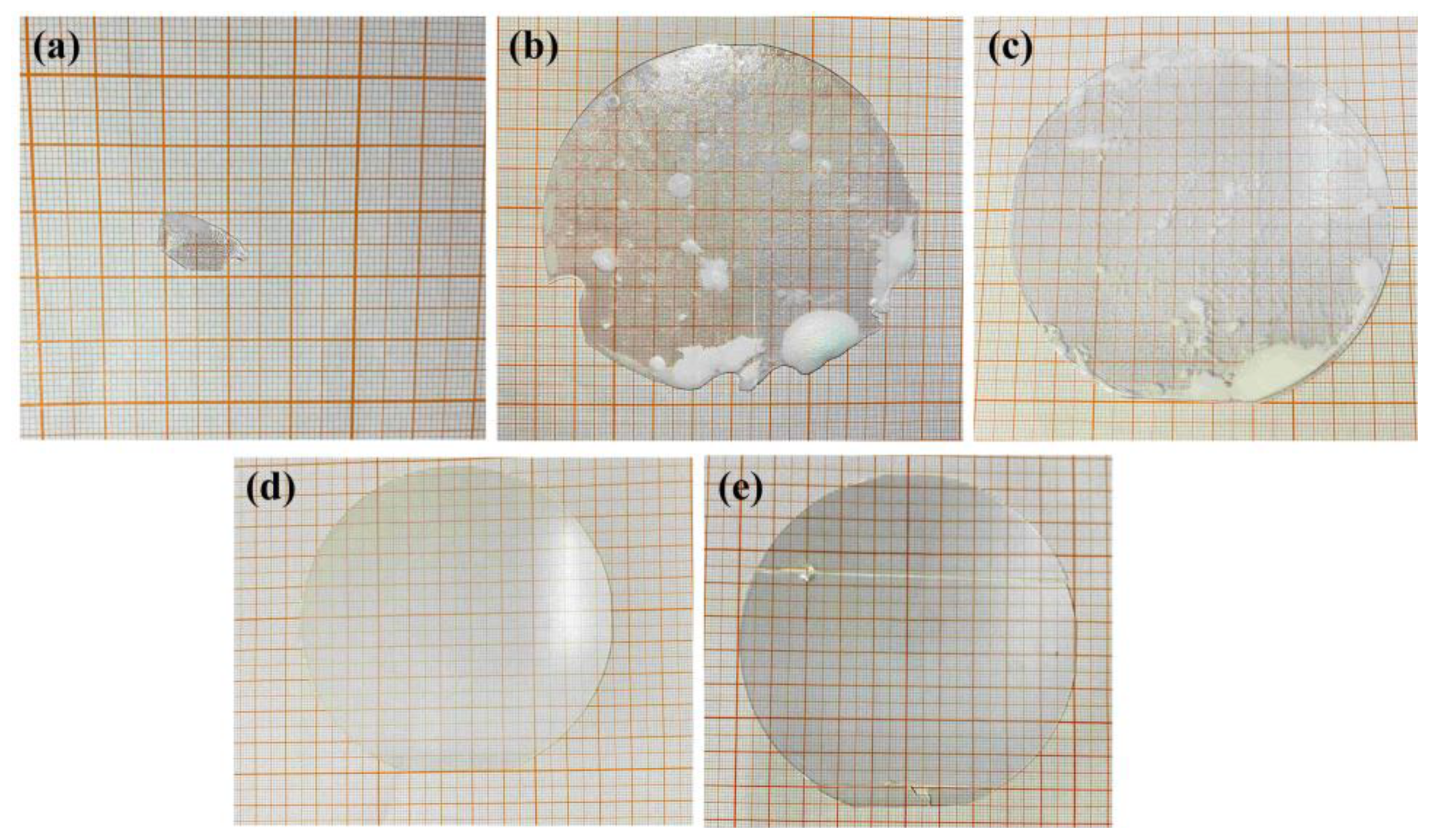
| Diffusion Powder | Holding Temperature | State of the Wafer to Be Diffused | As Shown in the Figure 3 |
|---|---|---|---|
| Li/Nb = 58/42 | 1210 °C | Almost all melted | Figure 3a |
| Li/Nb = 58/42 | 1195 °C | Mostly melted | Figure 3b |
| Li/Nb = 56/44 | 1195 °C | A small part is melted, the wafer is incomplete, d33 = 10.5 × 10⁻¹² C/N | Figure 3c |
| Li/Nb = 54/46 | 1180 °C | not melted, Complete, d33 = 10.8 × 10⁻¹² C/N | Figure 3d |
| Li/Nb = 56/44 | 1160 °C | Complete, d33 = 0 | Figure 3e |
| Sample | d33/(×10−12 C/N) |
|---|---|
| CLN | 9.7 |
| Non-polarized NSLN | 10.4 |
| Polarized NSLN | 10.8 |
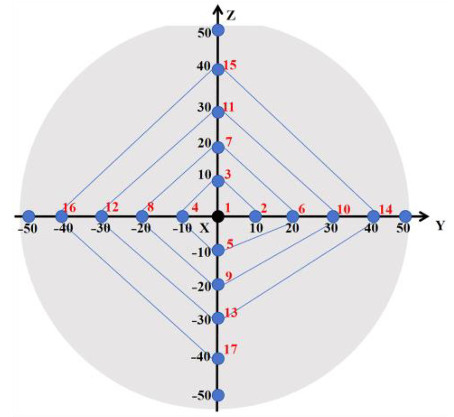
| Serial Number | Refractive Index n of NSLN (@632.8 nm) |
|---|---|
| 1 | 2.3044 |
| 2 | 2.2932 |
| 3 | 2.2992 |
| 4 | 2.3015 |
| 5 | 2.3035 |
| 6 | 2.2992 |
| 7 | 2.2920 |
| 8 | 2.2972 |
| 9 | 2.3006 |
| 10 | 2.2992 |
| 11 | 2.2845 |
| 12 | 2.3047 |
| 13 | 2.3001 |
| 14 | 2.3049 |
| 15 | 2.3044 |
| 16 | 2.3035 |
| 17 | 2.3017 |
| Average value | 2.2996 |
| Transverse meanΔn16-14 | 1.75 × 10⁻⁴/cm |
| Longitudinal meanΔn17-15 | 3.375 × 10⁻⁴/cm |
Disclaimer/Publisher’s Note: The statements, opinions and data contained in all publications are solely those of the individual author(s) and contributor(s) and not of MDPI and/or the editor(s). MDPI and/or the editor(s) disclaim responsibility for any injury to people or property resulting from any ideas, methods, instructions or products referred to in the content. |
© 2025 by the authors. Licensee MDPI, Basel, Switzerland. This article is an open access article distributed under the terms and conditions of the Creative Commons Attribution (CC BY) license (https://creativecommons.org/licenses/by/4.0/).
Share and Cite
Dong, Z.; Xu, Q.; Liang, S.; Si, J.; Wang, M.; Zhang, X.; He, J. Research on the Fabrication of X-Cut Near Stoichiometric Lithium Niobate Wafers. Crystals 2025, 15, 282. https://doi.org/10.3390/cryst15030282
Dong Z, Xu Q, Liang S, Si J, Wang M, Zhang X, He J. Research on the Fabrication of X-Cut Near Stoichiometric Lithium Niobate Wafers. Crystals. 2025; 15(3):282. https://doi.org/10.3390/cryst15030282
Chicago/Turabian StyleDong, Zixuan, Qingyan Xu, Shuaijie Liang, Jiashun Si, Mengfan Wang, Xuefeng Zhang, and Jilin He. 2025. "Research on the Fabrication of X-Cut Near Stoichiometric Lithium Niobate Wafers" Crystals 15, no. 3: 282. https://doi.org/10.3390/cryst15030282
APA StyleDong, Z., Xu, Q., Liang, S., Si, J., Wang, M., Zhang, X., & He, J. (2025). Research on the Fabrication of X-Cut Near Stoichiometric Lithium Niobate Wafers. Crystals, 15(3), 282. https://doi.org/10.3390/cryst15030282