3. Results and Discussion
Four different types of PSCs were designed and fabricated, each incorporating a different combination ofnonporous TiO
2, MP-TiO
2, and a buffer layer between the active layer and ETL. The detailed fabrication processes and characteristics of these PSCs have been previously reported [
26]. As illustrated in
Figure 1, this study focuses on the preparation of mesoscopic PSCs with various selective contacts. These architectures demonstrate the selective collection of electrons, which exhibit different mobilities as they traverse the ETL owing to variations in trap sites introduced by the nonporous TiO
2, MP-TiO
2, and buffer layer. Among the four different device structures depicted in
Figure 1,
Cell (b) exhibited the highest efficiency owing to relatively high current density (J
sc), open circuit voltage (V
oc), and fill factor (FF) (refer to
Figure 2a and
Table 1). Notably, the J
sc and FF were considerably enhanced compared to the other cells, leading to an improvement in overall solar cell efficiency [
26]. In contrast, the performance of
Cell (c) and
Cell (d) was reduced. Specifically,
Cell (c) exhibited a decrease in FF of approximately 20% compared to the other devices, indicating lower stability. The motivation of this study was to understand why the characteristics of solar cells differed considerably.
Upon illumination of the perovskite (MAPbI
3) material with sunlight, electron–hole pairs are generated in the material and subsequently injected carriers into the charge transport layer (refer to
Figure 3a). Charge separation and injection can occur via two primary pathways: (1) injection of electrons into the ETL [(e
−---h
+) MAPbI
3 perovskite → e
cb−(ETL) + h
+(MAPbI
3 perovskite) (step 1)] and (2) injection of holes into the HTL [(e
−---h
+) MAPbI
3 perovskite → h
+(HTL) + e
−(MAPbI
3 perovskite) (step 2)]. The carriers injected into the charge transport layers can undergo various processes, including exciton annihilation through photoluminescence [(e
−---h
+) MAPbI
3 perovskite → photoluminescence (step 3)] or non-radiative recombination [(e
−---h
+) MAPbI
3 perovskite → non-radiative recombination (step 4)]. Additionally, back charge transfer can occur at the ETL/MAPbI
3 layer interface [e
cb−(ETL) + h
+(MAPbI
3 perovskite) → recombination (step 5)] and the MAPbI
3 layer/HTL interface [h
+(HTL) + e
−(MAPbI
3 perovskite) → recombination (step 6)]. Finally, charge recombination can take place through the recombination of electrons in the ETL and holes in the HTL [e
cb−(ETL) + h
+(HTL) → recombination (step 7)]. Owing to the above-mentioned processes [steps (3), (4), (5), (6), and (7)], which can reduce the efficiency of PSCs, it is desirable for the carrier lifetime of MAPbI
3 to be prolonged. The implementation of a buffer layer, as depicted in
Figure 3b, can decrease the charge recombination rate and enhance the efficiency of PSCs. To mitigate charge recombination in MAPbI
3, we used a passivation effect by incorporating an Al-doped TiO
2 buffer layer between the CP-TiO
2(ETL)/MP-TiO
2 interface. The carrier lifetime (or simply the lifetime) generally refers to the duration during which a charge carrier remains free to move, thereby contributing to electrical conduction. Charge carrier lifetime (or effective electron lifetime,
τeff) refers to the duration that charge carriers (electrons in the conduction band and holes in the valence band) remain in a free state. It is defined as the average time taken for a minority carrier to recombine and can vary considerably depending on the materials and construction of the semiconductor. The energy released during recombination can manifest as heat or photons (optical recombination, used in LEDs and semiconductor lasers). Consequently, charge carrier lifetime is a critical factor in bipolar transistors and solar cells. The recombination lifetime (
τr) especially refers to the time frame for the recombination of injected or photogenerated electrons and holes. It serves as a fundamental parameter in the analysis of semiconductor optoelectronic devices, particularly solar cells. Surface recombination occurs at the top of the solar cell, emphasizing the importance of using material layers with superior surface passivation properties to minimize the impact of light exposure over periods. As illustrated in
Figure 1, MAPbI
3 possesses two distinct interfaces: the ETL/MAPbI
3 interface and the MAPbI
3/HTL interface. Minimizing the recombination rate of electrons and holes at each of these interfaces is crucial. Furthermore, it is essential to modulate the energy levels of the conduction and valence bands through techniques such as self-passivation, doping, and interlayer passivation, to enhance device performance.
In this study, our primary objective was to investigate the impact of various ETLs on the electron transfer ability of carriers generated in the active layer. Building upon our previous PL analysis [
26], which revealed a reduction in the PL area for
Cell (b) compared to other cells, we hypothesized that the rate of carrier recombination was influenced by the material properties, structure, and characteristics of the ETL. These factors can affect both the generation of excitons and the mobility of charge carriers. Our findings suggest that the presence of a buffer layer, such as Al-doped TiO
2, at the MAPbI
3/ETL interface facilitates the transfer of generated electrons to the electrode. This indicates an increase in carrier lifetime owing to enhanced recombination resistance. Consequently, the electron acceptor ability was enhanced when the PSC was fabricated using an Al-doped TiO
2 buffer layer. Conversely, in the
Cell (c) and
Cell (d) structures, the hindered generation of electrons impedes proper crystal growth. This suggests that in poorly formed crystals, these paration of electrons and holes is compromised, hindering charge injection [steps (1) and (2)], back charge transfer [steps (5) and (6)], and charge recombination [step (7)]. Instead, exciton annihilation [steps (3) and (4)] occurs at a considerably higher rate. These effects adversely impact the recombination rate, ETL functionality, and overall solar cell performance. To check this kind of passivation effect systematically, we first prepared the crystalline Al-doped TiO
2 buffer layers with different Al-doping concentrations based on
Cell (b). Then, the analysis of X-ray diffraction (XRD), Raman spectroscopy, and X-ray photoelectron spectroscopy (XPS) were sequentially utilized to prove the passivation effect as well as to understand the charge transfer behavior of the PSCs. For the analysis of XRD, we made all structures of perovskite without HTL, and the thickness of whole ETLs was fixed to 100 nm for both pure TiO
2 and Al-TiO
2 thin films.
Figure 4a shows XRD patterns of both pure crystalline TiO
2 and crystalline Al-doped TiO
2 thin films with different Al-doping concentrations. All observed peaks corresponding to TiO
2 can be attributed to the anatase (A) and rutile (R) phases of TiO
2, which were preserved upon the incorporation of Al precursor up to 10 mol%. No additional peaks associated with TiO
2 material were detected during the Al precursor doping process. The ionic radii of the Ti
4+, Ti
3+, and Al
3+ ions are 0.61, 0.64, and 0.53 nm, respectively. As Ti
3+ ions are replaced with Al
3+ ions, the unit cell size of crystalline Al-doped TiO
2 decreases compared to TiO
2. As we can see from the right-hand side figure of
Figure 4a, both the (101) anatase peak and the (110) rutile peak move slightly towards a higher degree as doping proceeds gradually, indicating that the unit cell is to expand its original size. In addition, the (110) rutile peak at 26.8 degreess harpens with increasing Al-doping concentrations up to 10 mol%, while the (101) anatase peak at 25.5 degrees broadens. The crystallite size of Al-doped TiO
2, calculated using the Scherrer equation, increases with the Al-doping concentration. Consequently, the incorporation of Al ions introduces stress into the TiO
2 lattice during the doping process, resulting in a slight shift in the peak positions toward higher degrees, indicating unit cell expansion.
Figure 4b shows the UV-Vis absorption spectra, which exhibit a shift toward shorter wavelengths with increasing Al-doping, a phenomenon known as
blue shift. This observation suggests the possibility of an increase in the conduction band energy level of the ETL owing to the blue shift effect. Consequently, the Fermi level in the device may be increased, leading to an enhancement in either V
oc or FF. Based on the Tauc-plots, which can be obtained from
Figure 4b, moreover, we observed a variation in reducing optical bandgap from 3.20 to 2.24 eV with increasing Al-doping concentration (mol% Al) between 0 and 7.Then, there will be further decreasing the optical bandgap up to 2.07 eV when 10 mol% Al is doped. This means that the conduction band (i.e., HOMO-energy level) of ETLs will be changeable as the Al-doping concentration is changed. In this study, we observed that the HOMO-energy levels of the ETLs gradually increase as the Al-doping content increases.
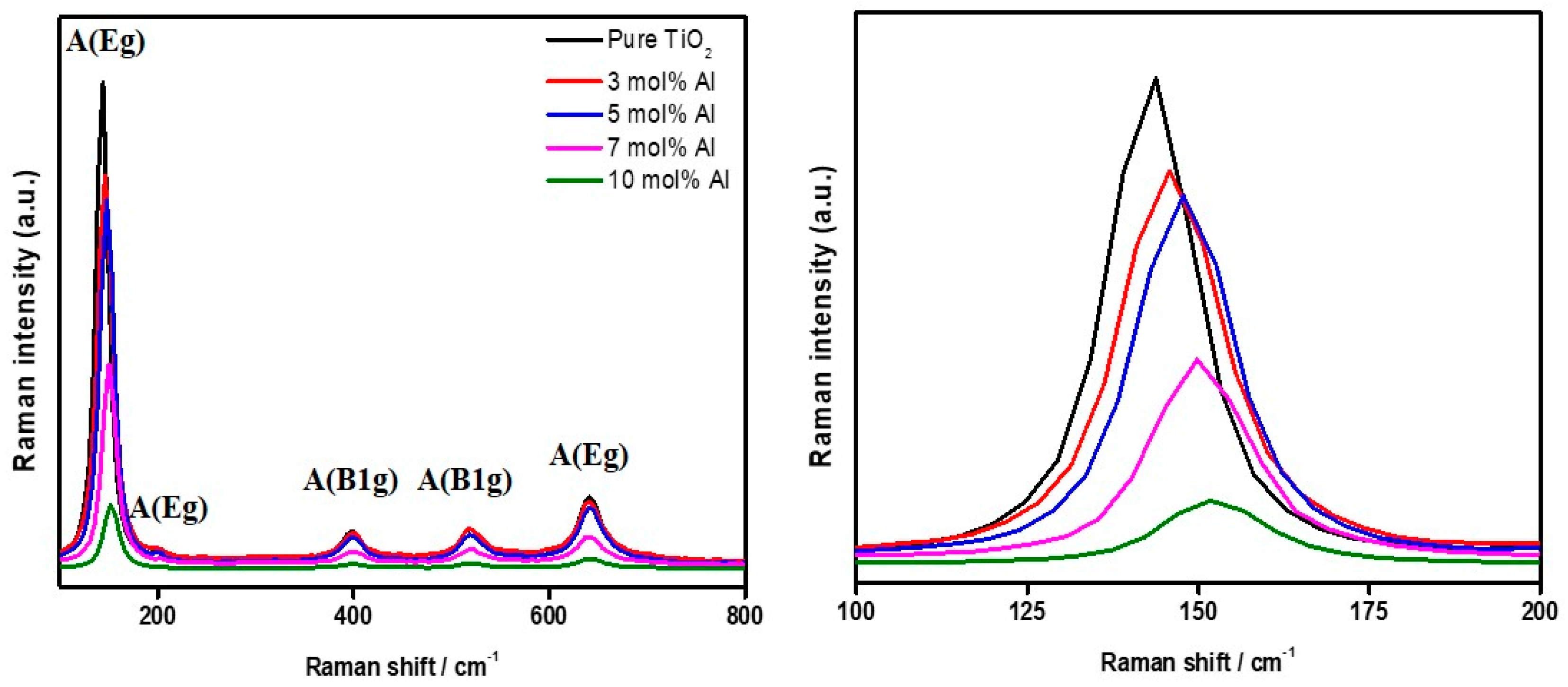
Figure 5 shows the Raman spectra of the crystalline Al-doped TiO
2 samples. Rutile and anatase phases were determined: Rutile peaks at 143 cm
−1 (B
1g), 447 cm
−1 (E
g), 611 cm
−1 (A
1g); Anatase peaks at 144 cm
−1 (E
g), 197 and 640 cm
−1 (E
g), 398 and 515 cm
−1 (B
1g), respectively. Notably, the primary active Raman mode (E
g) of the anatase phase was observed at 144 cm
−1, which corresponds to -Ti-Ti vibrations in the octahedral chains [
27]. Meanwhile, the active Raman modes reported for aluminum oxide at 384 and 417 cm
−1 were not detected, confirming the substitutional incorporation of Al into the TiO
2 crystalline structure [
27]. Another noteworthy observation is the decrease in the Raman intensity of TiO
2 associated with the vibrational modes of both anatase and rutile as the Al-dopant concentrations increase. Upon zooming in on the A(E
g) vibrational mode, the Raman peak intensities exhibit a decreasing trend with the following sequence of Al mol% contents: 0, 3, 5, 7, and 10 mol%, respectively (refer to the enlarged figures on the right-hand side). Additionally, the peak positions shift toward higher wavelengths (similar to the UV-visible result), indicating a relative decrease in bond length in the lattice for both anatase and rutile phases [
27]. Furthermore, the effects of Al-dopant incorporation into the TiO
2 crystalline structure can be observed through the changing trends of the primary active Raman mode (E
g) in
Figure 5. The decrease in peak intensity and shift toward higher wavenumbers (namely bathochromic shift) signify the grain boundary disorder of TiO
2 induced by Al-doping [
28]. Notably, despite the increasing Al-doping concentration, all Raman peaks associated with the anatase phase persist, while the rutile phase peaks gradually diminish. This suggests that the remaining peak may be attributed to the insertion of Al
3+ ions into the TiO
2 lattice. Liu et al. obtained similar results and identified a new Raman vibrational peak at approximately 317 cm
−1 in their Al-doped TiO
2 crystalline materials [
28].
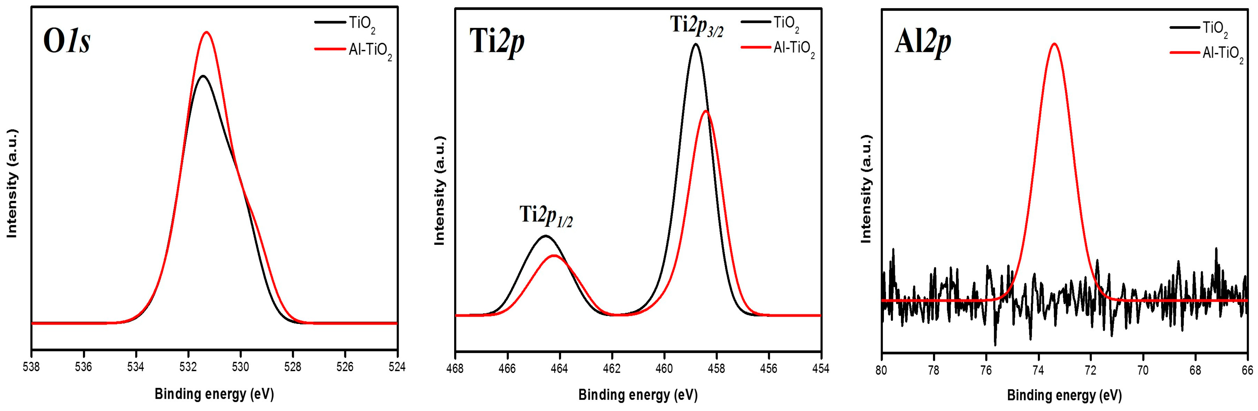
Al-doping was further corroborated by XPS. XPS was measured to confirm the changes in the oxidation number of O
1s, Ti
2p, and Al
2s in TiO
2 during the 7 mol% Al-doping process.
Figure 6 shows high-resolution XP spectra of O
1s, Ti
2p, and Al
2p for doped (red color) and undoped (black color) samples. The Al
2p peak (refer to the right-hand side figure) increases peak intensity in the Al (7 mol%)-doped TiO
2. However, no Al
2p peak was detected in the pure TiO
2 sample. In the pure TiO
2, the Ti
2p3/2 and Ti
2p1/2 peaks (refer to the middle figure) are located at binding energies of 458.8 and 464.5 eV, respectively. Upon the incorporation of Al into the TiO
2 crystalline lattice, the Ti
2p peaks exhibit a slight shift toward lower binding energy, indicating a reduced oxidation state compared toTi
4+ in pure TiO
2. The primary O
1s peak (refer to the left-hand side figure), with an asymmetric shape, is located at a binding energy of 529.0 eV and may correspond to bonding with both Ti and Al. Additionally, an O
1s peak with an asymmetric shape at 531.0 eV was identified and attributed to oxygen species in the Al-doped TiO
2 buffer layers. Only a minor shift toward a lower O
1s binding energy was observed, potentially resulting from the change in electronegativity of the Ti bond from -O-Ti to Al-O-Ti in the crystal structure of the buffer layer. Consistent with previous studies [
28,
29], the O
1s peak observed at approximately 529.0 eV exhibits an asymmetric shape for both pure and doped TiO
2, suggesting the presence of defect sites and/or potential surface contamination. This indicates that all our samples may have experienced a degree of contamination during the measurement process (or surface oxidation owing to exposure to air), leading to a chemical shift of up to 0.6 eV in the O
1s binding energy.
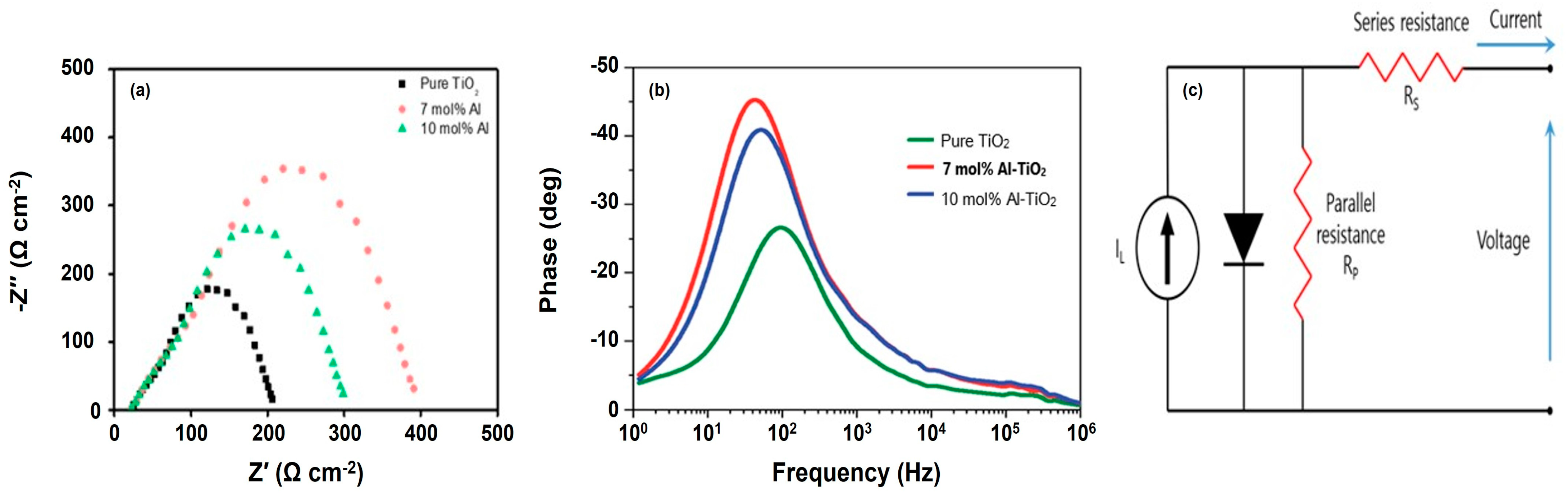
To check the detailed passivation effect of buffer layers with different Al-doping concentrations, the characteristics of solar cell devices, photocurrent density–voltage (I-V) curves shown in
Figure 2b were measured and their measured parameters are summarized in
Table 2. As shown in
Table 2 and
Figure 2b, the J
sc, V
oc, and FF parameters exhibit a gradual increase up to an Al-doping concentration of 7 mol%, contributing to an improvement in cell performance from 9.24% to 11.87%. This enhancement can be attributed to the smoother transfer of electrons from the MAPbI
3 layer to the electrode through the ETL. In the 7 mol% Al-doping range, the ECE shows a consistent increase, primarily owing to the increase in current density (J
sc). However, beyond 7 mol% Al-doping, the ECE increases. These observations suggest that the electron acceptor ability is enhanced by the Al-doping process below 7 mol%, indicating a reduction in the recombination rate and an increase in the Fermi-energy level with an appropriate amount of Al-doping. Consequently, the crystalline Al-doped TiO
2 buffer layer contributes to an improvement in recombination resistance. In general, photovoltaic performance parameters such as short-circuit current density, open-circuit voltage, and photon current conversion efficiency can be extracted from J-V measurements. While J-V measurements provide insights into the photovoltaic performance of solar cells, they do not offer information about photoelectrochemical behavior such as series and charge transfer resistance, electron lifetime, and charge collection efficiency. These parameters can be obtained using EIS. EIS measurements generate the Nyquist plot (see
Figure 7a) as well as the Bode plot [refer to
Figure 7b], which depict the charge transfer resistance (R
r or R
ct) and angular frequency (ω
rec) for the solar cell under study.
To prove this, therefore, the EIS analysis for the three fabricated PSCs without and with buffer layers was performed. As we can see in
Figure 7a, the EI spectra of PSCs contain two RC arcs. One is related to the contact resistance of the interfaces at high frequency with the same area. The other is attributed to recombination resistance and chemical capacitance (C
μ) of the device at low frequencies [
30]. Thus, EIS results can give the values of both charge transfer resistance that can induce with C
μ and recombination resistance at the ETL/MAPbI
3 interfaces and MAPbI
3/counter electrode in the field of PSC. For example, the reduction in frequency in the EIS measurement generated a higher electron lifetime, which is explained in Equation (5) and
Table 3. In this scenario, the relationship is inversely proportional to the maximum frequency. For the analysis of EIS data, both the Bode plot depicted in
Figure 7b and a traditional equivalent circuit model depicted in
Figure 7c were also utilized in his study. As shown in
Figure 7c, a constant photo-generated current source, a series parasitic resistance (i.e., series resistance, R
s), and a parallel parasitic resistance (i.e., parallel resistance, R
p) are also generally included. When comparing the J-V results with the EIS data presented in
Figure 7a, it is evident that the PSC with the 10 mol% crystalline Al-doped TiO
2 layer exhibits higher R
s and lower recombination resistance compared to the PSC with the 7 mol% crystalline Al-doped TiO
2 buffer layer. This indicates a decrease in carrier transport ability owing to a relatively high Fermi-energy level of the ETL, suggesting that electrons encounter difficulty in overcoming the energy barrier. Consequently, exciton annihilation [steps (3) and (4)] and back charge transfer [step (6)] become more likely to occur, while electron injection [step (1)] is hindered. This ultimately leads to electron–hole recombination. As the Al-doping concentration increases, the HOMO-energy level of the ETL gradually increases. The PSC with the 7 mol% crystalline Al-doped TiO
2 buffer layer demonstrates the most efficient charge injection [step (1)] and minimal back charge transfer [step (5)] as a result of the
passivation effect. This observation confirms that the solar cell parameters with the 7 mol% crystalline Al-doped TiO
2 buffer layer were improved, leading to the best cell performance (11.87%) in comparison to the non-doping sample (6.37%). However, the solar cell performance declined with the 10 mol% crystalline Al-doped TiO
2 sample. This suggested that the conduction band energy level became excessively high, making it more challenging for electrons to move through the ETL, thereby increasing the recombination rate. To clarify these aspects, we performed theoretical calculations to obtain various electron transport parameters as follows.
Based on the diffusion-recombination transmission line model, the measured impedance in
Figure 7a is attributed to the following equations [
31,
32,
33,
34].
where Z represents the electrochemical impedance for the photoanode thin film,
i = (−1)
1/2, ω denotes the angular frequency, ω
rec signifies the frequency of the charge transfer process, R
t is the transport resistance of the electrons and R
r is the charge transfer resistance associated with the recombination of electrons at the perovskite/HTL interface. R
r can also be referred to as the charge transfer resistance (R
ct) [
34]. Additionally, Equation (1) reveals the relationship between two opposing processes that occur in solar cells: electron transfer across the semiconductor layer (ω
d) and carrier loss owing to electron recombination (ω
rec). These processes can be mathematically expressed as follows:
where D
eff represents the effective electron chemical diffusion coefficient, L is the thickness of the photoanode film layer, L
n is the effective electron diffusion length of the photoanode, and C
μ denotes the chemical capacitance, respectively [
31,
33]. When R
t ≪ R
ct or ω
rec ≪ ω
d, the parallel connection of R
ct and C
μ results in the formation of a recombination arc, and Equation (1) can be simplified to the following form:
The small and large arcs of a conventional Warburg impedance appear at high and low frequencies, respectively, as shown in
Figure 7a. A large arc corresponds to a low or slower recombination effect compared to electron diffusion through the TiO
2 layer. Furthermore, R
t ≪ R
ct is a desirable condition for optimal solar cell performance because a large R
ct contributes to reduced electron recombination in the cell. Conversely, when R
t ≫ R
ct or ω
rec ≫ ω
d, a considerable combination effect arises in the solar cell owing to the Gerischer impedance, leading to the impedance curve with a smaller arc at high frequency as observed in
Figure 7a. Consequently, the recombination time is shorter than the electron diffusion across the TiO
2 layer. Based on the above-mentioned model theory, various electron transport parameters, such as the effective electron lifetime (
τeff), maximum peak frequency (f
max), and effective rate constant (k
eff) for recombination, can be extracted from the impedance spectra of solar cells. For instance,
τeff is derived from the f
max of the impedance spectra [refer to
Figure 7b], which corresponds to the photoanode in the medium frequency region [
35]. This maximum frequency also represents the effective rate constant (k
eff) for recombination. These three parameters are interrelated as follows:
This implies that the effective electron lifetime (
τeff) aligns with the angular frequency at the apex of the arc in
Figure 7a, expressed as ω
rec = 2πf
max = τ
eff−1, where ω
rec denotes the angular frequency of the electron recombination reaction [
36]. Equation (6) effectively elucidates the separation of a lifetime into two primary components. The separation occurs because R
rec encompasses both a density term, (the chemical capacitance) and a kinetic constant (k
eff). Consequently, the product in Equation (6) isolates the latter. The electrochemical capacitance (C
μ), which is linked to minority carrier accumulation, and the recombination resistances together yield a virtually constant lifetime across varying illumination intensities. In the presence of impurity levels, for instance, lifetimes in silicon exhibit high variability [
37], which is evenmore pronounced in amorphous inorganic semiconductors such as Al-TiO
2. It is crucial to emphasize that recombination constitutes an interfacial charge transfer event occurring at the boundary between the semiconductor and ionic/hole carrier. Given that the distance for electron tunneling is typically approximately 1 nm, which is considerably smaller than the average size of nanoparticles in a solar cell, it is beneficial to differentiate between bulk traps. In any transient measurement used to determine lifetime, a modification of the Fermi level entails a change in the occupancy of bulk traps. Consequently, we can derive the free electron lifetime (
Tt) by multiplying two experimentally determined quantities: the diffusion coefficient (D
n) and the effective electron lifetime (τ
eff). However, in this study, we used the values of the effective electron chemical diffusion coefficient (D
eff) as obtained theoretically.
The denominator of Equation (7) represents a constant estimated to be
D0 = 0.4 cm
2s
−1 [
38]. It has been well established that the mobility–lifetime product corresponds to the free carrier recombination time in amorphous silicon solar cells. Consequently, the electrochemical capacitance (C
μ) was also calculated using Equation (8), utilizing the values of τ
eff and R
ct extracted from the Nyquist plot.
Hence, the effective electron chemical diffusion coefficient (D
eff) and effective electron diffusion length (L
n) of the photoanode can also be derived from Equation (9) [
36].
This implies that the electron diffusion length (L
n) can be derived from Equations (3) and (4) and is determined by the product of the diffusion coefficient (D
eff) and the electron lifetime (
τeff). Based on Equation (9), we observe that L
n increases with increasing electron lifetime, assuming that the diffusion coefficient (D
eff) remains constant at a fixed temperature. It is also noteworthy to examine the observed properties of L
n in our solar cell devices. We initially note that L
n is not a transient quantity, but rather a steady-state parameter; therefore, it can be expressed in terms of the IS resistances as L
n = L(R
rec/R
t)
1/2, where R
t represents the transport resistance [refer to Equation (2)]. Consequently, bulk traps do not interfere with the diffusion length. Notably, the solid hole conductor OMeTAD (HTL) cell exhibits the lowest charge transfer resistance, which considerably impairs performance despite the cell’s attainment of higher photovoltage [
39,
40]. The model predicts that L
n is proportional to the square root of the free carrier lifetime. In solar cells, the diffusion length typically exhibits a slight increase with increasing bias voltage. For instance, for MP-TiO
2 with MP-TiO
2/Perovskite/HTL interface, the diffusion length is observed to increase with voltage in the absence of illumination, while a contrasting trend is observed under illumination: it decreases with the potential [
38,
39,
40].
In addition, we can determine the recombination lifetimes (
τr) from a photovoltage (V
oc) decay curve [
41] shown in
Figure 8.
Figure 8 is the photovoltage decay curve plotting 1/V
oc and J
sc as a function of Al-doping amounts in mol%, and realizes a tendency to oppose between
τr and
τeff (see
Table 3).
Table 3 summarizes the experimentally and theoretically obtained PSC parameters, including charge transfer resistance (R
ct), maximum peak frequency (f
max), effective electron lifetime (τ
eff), effective rate constant (k
eff) for recombination, effective electron chemical diffusion coefficient (D
eff), electrochemical capacitance (C
μ), free electron lifetime (T
t), effective electron diffusion length (L
n), and recombination lifetime (τ
r). From
Figure 7a,b, we can determine the R
ct and ω
rec values, and by using Equation (6), ω
rec = 2πf
max = τ
eff−1, we could obtain f
max values as well as τ
eff values which are listed in the 2nd and 3rd columns, respectively. As we can see in the 3rd column, the obtained
τeff values are 3.016 × 10
−3 s for 0 mol% Al-doping, 7.271 × 10
−3 s for 7 mol% Al-doping, and 4.398 × 10
−3 s for 10 mol% Al-doping, respectively. In contrast, the
τr values are 1.29 (0 mol%), 0.97 (7 mol%), and 1.12 s (10 mol%), respectively. The increase in
τeff facilitates electron diffusion and transfer owing to the increase in L
n, because
τr is closely related to both free electron lifetime (T
t) and electron diffusion length (L
n), as well as electrochemical capacitance (C
μ). The response time for recombination, commonly referred to as the “lifetime”, invariably comprises a recombination resistance and a capacitance, and it is directly revealed by IS measurement. However, the time constant of the recombination arc of IS must generally be expressed as
τr = R
recC
μ [
31]. The nature of the electrochemical capacitance (C
μ) is crucial for correctly interpreting τ
r as a lifetime. Under specific conditions, the transient measurement induces charging or discharging of the depletion layer in a Si-based solar cell, resulting in the measured “lifetime” having no correlation with recombination time. In such cases, the
τr values correspond to depletion capacitance and cannot be associated with the minority carrier lifetime. It is important to emphasize that when determining electron lifetime in solar cell devices, it is essential to verify that the recombination resistance is indeed associated with interfacial charge transfer at the nanostructured metal oxide [
42]. Carrier recombination lifetimes are often regarded as indicators of perovskite film quality, with longer decay lifetimes being associated with higher-performing materials. Carrier recombination kinetics has been characterized as a combination of trap-assisted, monomolecular (first-order), and bimolecular (second-order) recombination processes. While most studies agree that radiative bimolecular recombination is dominant at high initial carrier densities (
n0 > 10
17 cm
−3), reports on kinetics at lower excitation densities (relevant to solar cell operation) vary from single-exponential to bi-exponential and to stretched-exponential functions with varying degrees of accuracy [
43].
As evident from
Table 2 and
Table 3, our highest performing PSC with a 7 mol% crystalline Al-doped TiO
2 buffer layer exhibited the R
ct of 258.73Ω along with a low effective rate constant (k
eff) of 137.533 s
−1 for recombination. It also demonstrated a relatively long effective electron lifetime (τ
eff) of 7.271 ms (accompanied by a maximum electrochemical capacitance value of 28.10 μF) among the various solar cell devices. This is potentially attributable to the suppression of recombination, as indicated by the minimal recombination lifetime (0.97 s) and electron chemical diffusion coefficient (11.77 cm
2s
−1) at the CP-TiO
2(ETL)/Buffer layer(Al-doped TiO
2)/MP-TiO
2/Perovskite/HTL interfaces. Consequently, a relatively long effective electron diffusion length (
Ln) of 85.61 μm is achieved. Mahmud et al. observed that halide perovskite-based solar cells using a nano-mesoporous TiO
2 layer exhibited a slower decay rate, which translates to a longer effective electron lifetime, reduced charge recombination with enhanced charge collection efficiency [
44]. Similarly, Xiao et al. reported relatively long charge carrier lifetimes under 0.3 sun illumination [
45]. Carrier lifetimes in the microsecond range suggest a lack of non-radiative pathways, and such extended carrier lifetimes can fundamentally lead to high V
oc. We speculate that the primary factor contributing to the extended carrier lifetimes is a combination of enhanced perovskite crystal grain size and effective passivation achieved through the crystalline Al-doped TiO
2 layer [
46]. Two plausible explanations can be offered for the increased charge carrier lifetime. First, owing to the crystalline Al-doping of the TiO
2 buffer layer located between the pure TiO
2 and perovskite layer, the concentration of deep trap states, which serve as recombination centers, diminishes with increasing Al content. Consequently, the effective charge carrier lifetime is prolonged owing to a reduction in Shockley–Read–Hall (SRH) recombination. Second, the incorporation of Al-TiO
2 into the perovskite MAPbI
3 lattice may introduce additional defects, which are shallow in nature and act as dopants for the MAPbI
3 lattice. Unlike deep trap states located in the middle of the band gap, shallow traps positioned near the conduction or valence band of the semiconductor partially trap charge carriers, which must then be released back into the band prior to recombination. In this scenario, up to a certain doping level, the charge carrier lifetime would be extended because thetrapping-and-release events would decelerate the actual recombination process. Yang et al. reported that the CH
3NH
3Br-treated PSCs exhibited improved charge collection and surface passivation properties, possibly owing to reduced defect states [
47].
Based on our comprehensive experimental observations, we propose a plausible mechanism for the Al-doping processes in TiO
2 buffer layers as follows. As depicted in
Figure 9, when oxygen vacancies or Ti interstitials arise in the TiO
2 lattice, Ti ions are preferentially substituted by Al ions in substitutional sites rather than interstitial sites. This substitution triggers the transformation of Ti(IV) into both Ti(III) and Ti(IV)
+ + e
− forms owing to the presence of defect [refer to
Figure 9a]. Subsequently, Ti(III) is replaced by Al(III), which exhibits enhanced stability, leading to changes in optical and electrical properties [refer to
Figure 9b]. In a solar cell, an electrical device, semiconductors such as Si, TiO
2, and perovskite material are subjected to light, which is converted into electricity via the photovoltaic effect. Electrons are either excited through the absorption of light, or if the material’s bandgap energy can be bridged, electron–hole pairs are generated, simultaneously creating a voltage potential. Consequently, charge carrier and electron diffusion, as well as electron recombination events, frequently occur in a solar cell. The charge carriers in the solar cell move through the semiconductor to counteract the voltage potential, which serves as the drifting force for electron movement. Additionally, electrons can be forced to move by diffusion from areas of higher electron concentration to areas of lower electron concentration. Therefore, to optimize the efficiency of a solar cell, it is highly desirable to collect as many charge carriers as possible at the cell’s electrodes. This implies that electron recombination, which can compromise solar cell efficiency, must be minimized. Consequently, we should prioritize increasing carrier lifetime while maintaining minimal electron recombination, suggesting that steps 1 and 5 in
Figure 3 are of greater significance than the other steps. By successfully growing higher-quality crystals with minimal defects, we can achieve considerably higher ECE than current levels. This occurs because efficient electron–hole separation is hindered in a defective crystal lattice. Additionally, steps 3 and 4 in
Figure 3 will proceed at a faster rate, which can adversely impact the recombination rate, ETL, and overall solar cell performance.


