Article

Synthesis and Mechanism Study of Carbon Nanowires, Carbon Nanotubes, and Carbon Pompons on Single-Crystal Diamonds

1
School of Materials Science and Engineering, Chongqing Jiaotong University, Chongqing 400074, China
2
School of Aeronautics, Chongqing Jiaotong University, Chongqing 400074, China
3
Jihua Laboratory, Foshan 528200, China
*
Author to whom correspondence should be addressed.
Crystals 2024, 14(6), 481; https://doi.org/10.3390/cryst14060481
Submission received: 22 April 2024 / Revised: 16 May 2024 / Accepted: 17 May 2024 / Published: 21 May 2024

Abstract

:
Carbon nanomaterials are in high demand owing to their exceptional physical and chemical properties. This study employed a mixture of CH4, H2, and N2 to create carbon nanostructures on a single-crystal diamond using microwave plasma chemical vapor deposition (MPCVD) under high-power conditions. By controlling the substrate surface and nitrogen flow rate, carbon nanowires, carbon nanotubes, and carbon pompons could be selectively deposited. The results obtained from OES, SEM, TEM, and Raman spectroscopy revealed that the nitrogen flow rate and substrate surface conditions were crucial for the growth of carbon nanostructures. The changes in the plasma shape enhanced the etching effect, promoting the growth of carbon pompons. The CN and C2 groups play vital catalytic roles in the formation of carbon nanotubes and nanowires, guiding the precipitation and composite growth of carbon atoms at the interface between the Mo metal catalysts and diamond. This study demonstrated that heterostructures of diamond–carbon nanomaterials could be produced under high-power conditions, offering a new approach to integrating diamond and carbon nanomaterials.

1. Introduction

Since the discovery of carbon nanomaterials, their unique physical and chemical properties, such as high strength, excellent conductivity, thermal conductivity, chemical stability, and high surface area, have been researched extensively. Carbon nanomaterials are generally composed of only one shape, such as graphene sheets [1], carbon nanotubes (CNTs) [2], carbon nanofibers [3], carbon nanospheres [4], carbon nanorods [5], fullerene [6], carbon onions [7], and other shapes [8]. Carbon nanomaterials have been found to have increasing applications in ion batteries [9], adsorbents [10], energy storage, catalysis, biomedicine [11], environmental governance, and water treatment. Lin et al. [12] reported that SiOC (Fe) ceramics could generate a large number of carbon nanowires (CNWs) during long and multiple insulation processes and slow heating processes. These CNWs not only form a conductive network, improve the conductivity, and increase the macroscopic current caused by charge carriers, but also effectively improve the dielectric loss of the material, promoting the conversion of electromagnetic energy into thermal energy. Diamond, an allotrope of carbon, is popular as a gemstone because of its hardness and color. In addition to natural diamonds, laboratory-grown artificial diamonds show chemical stability, high thermal conductivity (24 W/cm·K) [13], high carrier mobility (9.5 MV/cm) [14], and a low dielectric constant. Therefore, diamonds have been extensively studied for applications in electronic devices [15], thermal management, diffractive optical elements [16], and biomedicine [17]. In most applications, carbon nanomaterials are grown on substrates, such as silicon carbide, graphite, platinum, and nickel [18,19,20]. Existing evidence suggests that the heterostructure of graphene and diamond is beneficial for many applications. Gu et al. [21] demonstrated that graphene could be grown from diamonds based on first-principle calculations, which provided a theoretical foundation for a simple method to prepare a diamond–graphene heterostructure and avoid the complex procedures of graphene transfer. Unpolished (111) single-crystal diamond synthesized under high pressure and high temperature (HTPT) was used as the substrate. A mixture of CH4, H2, and boron-doped sources was introduced to hot-filament chemical vapor deposition (HFCVD) to grow boron-doped diamond films; graphene was shown to form spontaneously after doping. The diamond–graphene heterostructure possessed a mobility of 1.0767 × 104 cm2/V·s at room temperature, higher than most reported graphene materials. The formed graphene replicated the symmetry of diamond (111), showing complete symmetry in theoretical simulations with no defects and no floating regions. This homogeneous structure combines the intrinsic properties of graphene and diamond while controlling the number of graphene layers. This opens up the possibility of using graphene–diamond heterostructures to fabricate high-performance devices in the future.
Various techniques have been employed for synthesizing carbon materials, such as laser sputtering, combustion, and chemical vapor deposition (CVD). The versatility and efficacy of these methods can create a variety of carbon-based materials with distinct properties and applications. Ismail et al. [22] embarked on a novel synthesis endeavor aimed at producing multi-walled carbon nanotubes (CNTs) alongside carbon nanoparticles. This process involved subjecting graphite targets to laser ablation within a water medium, all the while employing lasers emitting at varying wavelengths. What sets this method apart is its distinctive characteristic of not requiring any catalysts to initiate or facilitate the synthesis process. Interestingly, by leveraging lasers operating at different wavelengths, specifically 523 nm and 1064 nm, discernible differences were observed in the resultant CNTs. Notably, CNTs synthesized using the 523 nm laser exhibited higher absorbance compared to those generated with the 1064 nm laser. This discrepancy in absorbance levels hints at potential disparities in the structural and optical properties of the CNTs, suggesting that the choice of laser wavelength plays a crucial role in determining the final characteristics of the synthesized carbon nanostructures. Oulanti et al. [23] successfully produced CNTs through combustion processes. By depositing ferrocene as a catalyst on carbon fibers, the growth of CNTs was initiated within 0.4 s and could proceed under atmospheric pressure and low temperatures. As the catalyst density decreased, the diameter of the CNTs gradually increased, highlighting the significance of catalyst density in regulating nanotube growth. Similarly, Panickar et al. [24] reported the synthesis of carbon spheres (CS) using CVD techniques. By controlling the temperature at 1223 K, a relatively uniform deposition process was achieved. Moreover, an increase in the hydrogen concentration enhanced the graphitization. One of the key advantages of this approach was its high yield, with the ability to produce 1–2 g of CS in 30 min. Fernandes et al. [25] employed a microwave plasma chemical vapor deposition (MPCVD) technique coupled with the continuous administration of an iron catalyst. Through this method, they successfully synthesized carbon hybrid materials containing both nanocrystalline diamond and carbon nanotubes (CNTs). The integration of MPCVD, along with the sustained delivery of the iron catalyst, facilitated the successful fabrication of these hybrid materials. CVD [26] is a process of depositing materials onto a substrate by passing desired gases as precursors to react chemically with the surface of the substrate. This produces a stable surface coating with a uniform thickness. Therefore, this is the primary method for growing carbon nanomaterials. However, this method has some drawbacks. For example, the impurity in the carbon sources and gases or the contamination caused by the incomplete reaction of gases during heating can degrade the performance of the carbon nanomaterials. In HFCVD, the reactions between the hot metal wires and oxygen or highly corrosive gases can cause contamination. In contrast, in MPCVD, plasma is produced by microwave energy in the reaction chamber, where gas molecules interact with plasma and achieve increased internal energy, and the electrons in the gas molecules are excited to energy levels sufficient for ionization. This method allows the gas to be highly ionized under certain conditions, eliminating contamination and allowing the formation of highly pure materials. Therefore, MPCVD is almost exclusively used to grow diamonds [27]. This technique typically involves a controlled process wherein a moderate quantity of hydrogen is passed alongside the carbon source, constituting approximately 3–10% of the overall flow. This setup ensures that the hydrogen plasma effectively etches the graphite structure while maintaining stability in deposition, owing to the inert characteristics inherent in diamond formation. Contrarily, when it comes to the growth of carbon nanomaterials, a divergent approach is adopted. Here, the emphasis shifts towards circumventing the intense etching effect induced by the hydrogen plasma. Consequently, the proportion of the carbon source in the hydrogen flow is notably higher compared to that in the diamond growth process. This adjustment in the flow ratio is pivotal for fostering the growth of carbon nanomaterials without them succumbing to excessive etching, thereby facilitating the desired structural and morphological characteristics in the synthesized nanostructures.
The heterogeneous structure of graphene and diamond has received a lot of attention because graphene has high mechanical strength. Despite the difficulty in depositing graphene on mechanical parts, graphene can be grown on diamond-coated tools, and the formation of super-strong covalent bonds can eliminate the exfoliation. Lin et al. [28] proved that this heterogeneous structure reduces the cutting force of the tool by 40% and the wear of the tool surface by 20%. Other heterostructures of carbon materials and diamonds have also attracted attention because they combine the excellent properties of carbon materials and diamonds [29,30]. Similarly, all-carbon heterostructures have been used to fabricate emitters as coherent single-electron sources in vacuum nanoelectronics and electron quantum optics [31]. Lee et al. [32] employed both the electrostatic self-assembly (ESA) method and a conventional photolithography process to meticulously fashion electrode patterns onto boron-doped diamond (BDD). The catalysts utilized for the selective growth of carbon nanotubes (CNTs) on the BDD surface consisted of stainless-steel nano-ions containing Fe and Ni, which were administered in conjunction with the hot-filament chemical vapor deposition (HFCVD) technique. Subsequent electrochemical examinations unveiled a remarkable augmentation in the effective electrode area, surpassing that of BDD alone by approximately 16 times. The choice of glucose as the analyte provided a platform to scrutinize the biosensing capabilities of this heterostructure. Impressively, the hybrid configuration displayed a heightened sensitivity of 7.3 µA mM−1 cm−2 (with a correlation coefficient of R = 0.9943) and exhibited a notably expanded linear detection range when compared to BDD alone. It is pertinent to note that the discussion surrounding carbon nanomaterials extends beyond the realms of graphene and CNTs. While polycrystalline diamonds predominantly serve as substrates, an intriguing question persists: can carbon nanomaterials be cultivated on single-crystal diamonds, potentially yielding novel heterostructures with distinct properties and functionalities?
Tumilty et al. [33] demonstrated the feasibility of depositing CNTs on single-crystal diamond. In their experiment, a 1b diamond (100 HTHP) substrate was used, and a 20 nm thick Ni thin film was deposited on the substrate, which was monitored using thermocouples during growth. The introduction of a mixture of methane, hydrogen, and nitrogen enabled the successful growth of CNTs on single-crystal diamonds using the glow discharge technology. The discharge current and voltage were 75 mA and 390 V, respectively. The optimal growth temperatures and gas ratios were determined. Bokhonov et al. [34] demonstrated the possibility of growing aligned CNTs on the surface of diamond via CVD by heating nickelocene to 423 K and bringing it into the reaction zone through a flow of argon gas. However, MPCVD has not been used to grow carbon nanomaterials on single-crystal diamonds. In this study, we demonstrated that three types of carbon nanomaterials, i.e., carbon pompons (CPs), carbon nanowire (CNWs), and CNTs, were successfully obtained on single-crystal diamonds via MPCVD by appropriately adjusting the deposition parameters and substrate surface. The growth mechanisms of the three heterostructures were elucidated.

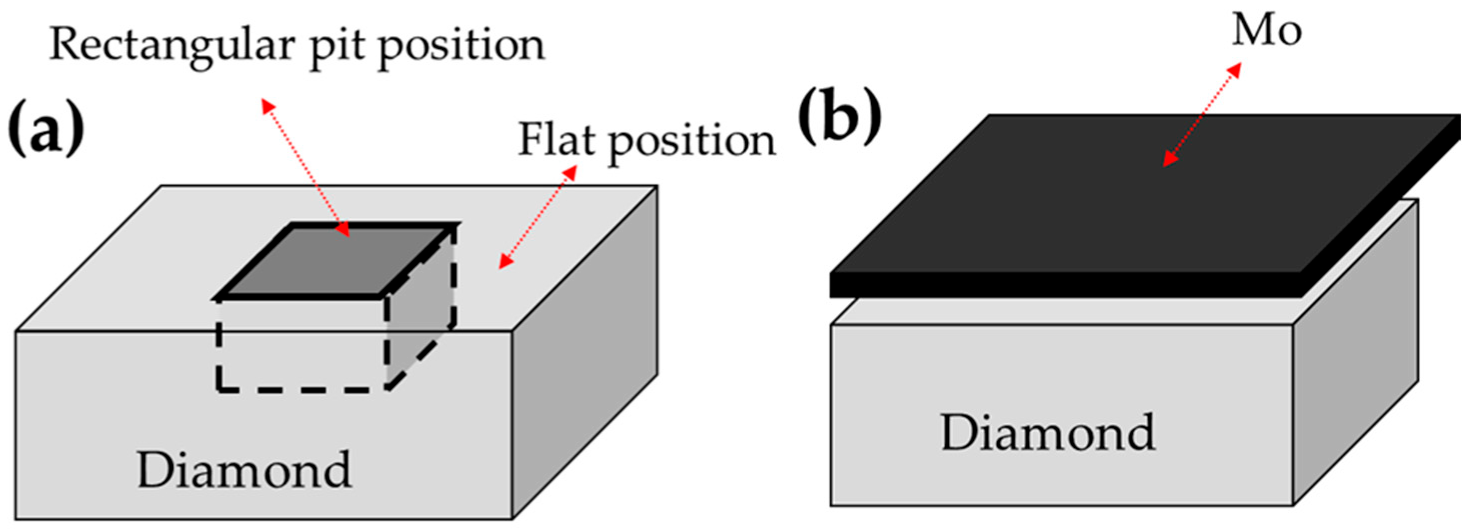
2. Materials and Methods

Continuous advancements in MPCVD equipment have led to the introduction of diverse chamber structures, including butterfly and cylindrical resonant chambers. In this study, a butterfly-shaped resonant cavity was employed. This specific chamber design enables the handling of power exceeding 10 kW and supports high-density plasma. Additionally, the reaction process pressure can reach up to 300 Torr. The selection of this particular chamber configuration highlights the significance of tailored equipment in optimizing plasma-enhanced processes for material synthesis. The microwave generator operated at a frequency of 2450 MHz and was capable of delivering an output power ranging from 1 kW to 13 kW. A reflection detector was integrated into a high-power load to quantify the magnitude of the reflection power. The substrate temperature was monitored using infrared temperature measurements in the range of 523–1673 K. Real-time temperature control was employed to maintain the temperature stability and mitigate the impact of temperature fluctuations. A series of experiments were conducted to identify the optimal parameters. For clarity, all of the experimental parameters and results are presented in Table 1. Experiments 1–4 were conducted on a 3 × 3 mm type IIb CVD (100) single-crystal diamond substrate. Prior to the experiment, a multistep wet chemical method was employed to clean the substrate. Briefly, the substrate was first heated at 473 K in a mixture of H2SO4 and HNO3 (1:1) for 20 min and subjected to ultrasonic treatment in deionized water for 15 min, in anhydrous ethanol for 15 min, in acetone for 15 min, and in anhydrous ethanol for 15 min, before drying with an argon gas gun. Experiments 1 and 2 were conducted using the same diamond substrate, as illustrated in Figure 1a. The substrate comprised a complete diamond with a rectangular pit on its surface, with dimensions of approximately 1 mm × 1 mm × 1 μm. Different surface conditions and temperatures of the diamond resulted in the deposition of two distinct carbon nanomaterials on the same diamond. CNTs typically grow on a catalyst spanning several tens of nanometers on a substrate surface. For experiments 3 and 4, a 150 nm Mo film was directly deposited on the diamond by magnetron sputtering, as shown in Figure 1b. Mo reacted with a carbon source during growth to form MoC [35], which acted as an effective catalyst and played a pivotal role in the controlled growth of carbon nanomaterials.
During the experiment, a fiber-optic probe was placed in a window outside the cavity and connected to an optical emission spectroscopy device (OES). This enabled the real-time detection of plasma in MPCVD using computer software. The surface morphology of the material was studied via high-resolution field-emission scanning electron microscopy (FE-SEM; JSM-6700F, JEOL, Prague, Czech, Europe). Transmission electron microscopy (TEM; FEI Tecnai 20, Brno, Czech, Europe) was used to further investigate the internal structure. Structural information on defects and deposits was analyzed using confocal laser Raman microscopy (Renishaw inVia Qontor, Ar ion laser, London, UK, 514.5 nm, 50 mW, spectral resolution ≤ 1 cm−1).

3. Results and Discussion

3.1. SEM Observations

Figure 2 presents the SEM images of various carbon nanomaterials deposited on the diamonds. As shown in Figure 2a, CPs of various sizes grow in the rectangular diamond pit with an average diameter of 20 μm. Some CPs exist separately, while others are connected. Figure 2b shows the image obtained outside the pit, wherein numerous carbon nanospheres (CNPs) are observed without the presence of CPs. Two distinct materials were deposited on the same single-crystal diamond substrate because of their different positions. Based on the temperature measured by an integrated infrared temperature monitoring system, the temperature difference at different positions was approximately 323 K. It can be preliminarily concluded that the presence of rectangular pits causes the temperature difference during the sedimentation experiment. The temperature of the substrate is derived from the plasma sphere, and the presence of a rectangular pit leads to plasma-enhanced etching, resulting in a higher temperature [36,37,38]. Figure 2c,d show two different carbon nanomaterials obtained after experiments 3 and 4, respectively. The image shows that the average diameter of the CNWs is 80 nm, whereas the diameter of the CNTs is approximately 400 nm. Relative to the diamond substrate, the CNTs and CNWs grow vertically, and some of them exhibit slightly curved random growth. Hydrogen was introduced into the plasma during the heating and cooling processes, which lasted for 10 min each. Despite the strong etching effect of hydrogen on the carbon material, the CNT and CNW products were firmly adsorbed on the diamond substrate and could not be removed during an adhesive tape test. In Figure 2c, it is evident that the material is solid, whereas the central part of the product in Figure 2d is hollow. In experiments 3 and 4, N2 was introduced to promote the growth of carbon nanomaterials. According to the literature [39], N2 can form N plasma, which promotes the methane-splitting reaction and the growth of CNTs. In experiments 3 and 4, different amounts of nitrogen were introduced at a constant methane concentration, indicating that the nitrogen at 9 sccm could generate CNTs. No CNT growth was observed on the diamond at a low flow rate of N2. In addition to the flow rate, there were two other differences between experiments 3 and 4, namely temperature and power. The temperature of the detached sphere in the MPCVD equipment could only be coupled and adjusted using pressure and power. Consequently, the differences in the power and temperature may have led to different growth factors.

3.2. TEM Observations

Figure 3 presents TEM images illustrating the deposition of CP and CNW in experiments 1 and 3. In Figure 3a, we observe small carbon nanoparticles and lines adhering to the CP surface, attributed to H-plasma etching. This process promotes the growth of velvety structures on the CP surface, facilitating CP deposition. Comparing Figure 2c and Figure 3b, the CNW interior appears as a solid structure with black segmented defects. This comparison highlights the distinct features of CP and CNW, shedding light on their structural properties during the synthesis process.
According to existing reports, a method has surfaced for fabricating ordered and pristine carbon nanowires (CNWs) through the meticulous design of pore templates on diamond substrates. These templates serve as initial sites for CNW growth, resulting in the formation of a composite structure comprising both diamond and diamond-like materials. Conversely, our study takes a departure from this conventional approach by embracing a template-free preparation method for CNW synthesis. By eschewing the need for pre-designed pore templates, our innovative technique simplifies the fabrication process while still achieving successful CNW production. This deviation from established methods not only broadens the spectrum of synthesis methodologies but also sheds light on alternative avenues for CNW fabrication.

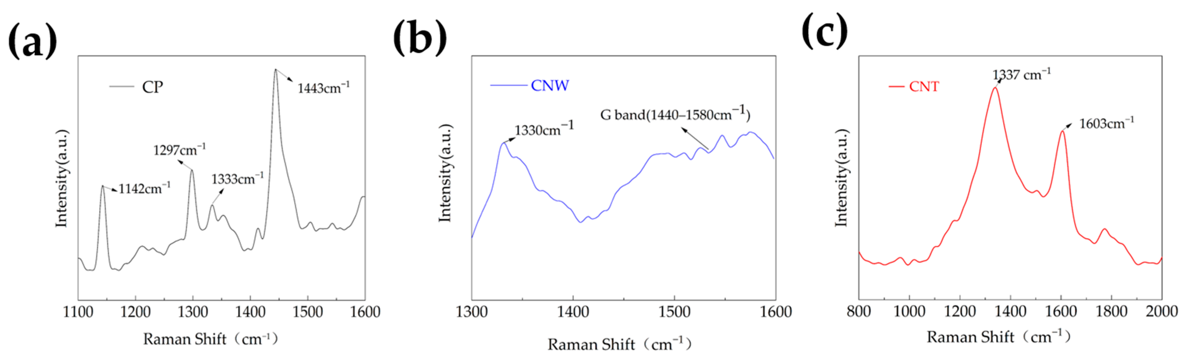
3.3. Raman Observations

Figure 4 illustrates the diverse micro-Raman spectra of different carbon nanomaterials to obtain valuable insights into molecular vibrations and crystal quality. Figure 4a shows the Raman spectrum of the CP deposited on a single-crystal diamond groove, wherein the diamond and graphene peaks emerge at 1333 cm−1 and 1443 cm−1, respectively. This is typically attributed to the substantial stress present in nanomaterials, which results in a shift in the Raman peak [40]. In addition, an evident defect peak is observed, which is responsible for the CP formation. The minor shoulder peak after the graphite peak also corresponds to disordered graphite structures [41], which do not manifest under defect-free conditions.
Figure 4b illustrates the appearance of a diamond peak at 1330 cm−1, accompanied by a broad graphite peak. This phenomenon is typically attributed to the formation of graphite through CVD [25,29]. In the presence of defects, the graphite peak results in a wide range of vibrational frequencies, and the sp3 peak position may be influenced by the diamond substrate. The spectrum of CNTs in Figure 4c shows the diamond peak at 1337 cm−1 and the graphite peak at 1603 cm−1. The blue-shifted peaks are related to the presence of stresses in CNTs, which is consistent with the literature [33].

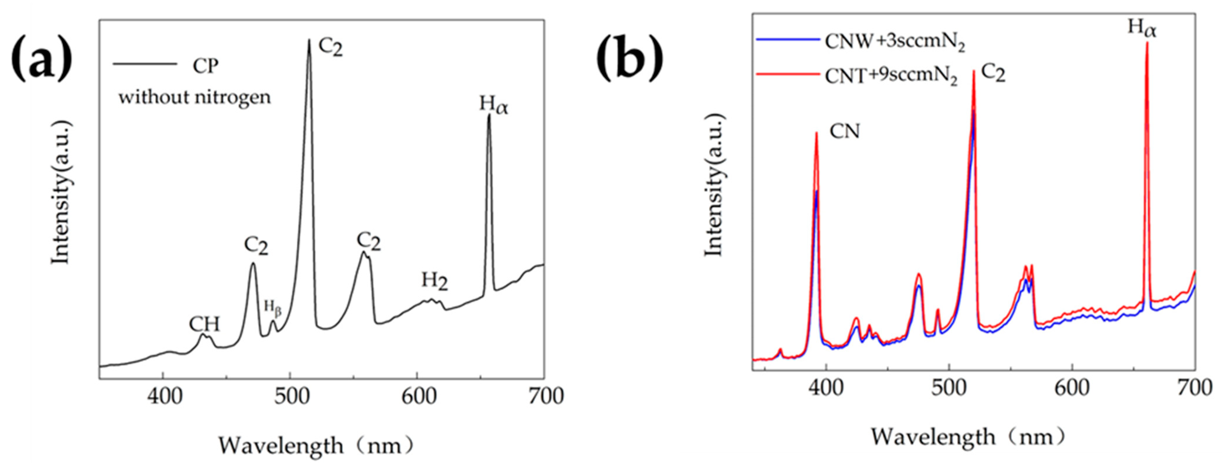
3.4. OES Observations

To gain insights into the deposition mechanisms of different carbon nanomaterials on diamond, OES testing was conducted on the plasma during the experiments. As shown in Figure 5a, a distinct C2 band was observed when methane and hydrogen were used to generate plasma. In experiments 3 and 4, the introduced N2 led to the formation of CN groups. The spectrum of CNTs had a stronger CN band, possibly because the higher N2 content in experiment 4 promoted the formation of C2 and the decomposition of methane [39].

3.5. Mechanism Research

For the gas phase, melting, or solution growth, the driving force (f) is closely related to the temperature. For example, gas-phase crystal growth can be expressed by Equation (1).
F = RTlnp/p0
where p is the gas-phase vapor pressure, p0 is the equilibrium vapor pressure, R is the molar gas constant, and T is the temperature. The crystal growth rate is determined by the driving force; the higher the driving force, the higher the growth rate. Temperature directly affects the morphology and crystallinity of CP materials. Considering that the temperature difference between the CNP and CP growth sites was 55 K (measured by the MPCVD infrared temperature measurement system), we made an inference of the growth mechanism of CP.
A deduced explanation for the growth mechanism of CP [42] is that CP is formed by stacking many carbon nanoparticles at lower temperatures. As the temperature rises to 1073 K, various factors, including the presence of diamond grooves, begin to influence the morphology of the plasma sphere. Figure 6 illustrates that this temperature increase accelerates the growth of different small carbon nanoparticles due to surface defects and plasma etching effects. With prolonged reaction times, particles initially present on the surface of the original carbon nanospheres gradually transform into carbon nanopillars with numerous “plush” features. Analysis of Raman spectra suggested that the abundance of defects may alter the growth rate of carbon nanoparticles, resulting in the formation of “plush” structures on the surface.
Experiments 3 and 4 utilized Mo thin films as the catalyst. Mo remains stable under high-temperature conditions, thereby promoting the growth of diamond surface products. The growth models for CNWs and CNTs [43] can be categorized into three types: top growth, bottom growth, or a combination of both. When the interaction between the catalyst and the substrate is weak, the carbon atoms dislodge from the catalyst and continue to grow. In contrast, the bottom growth model represents a stable combination of the substrate and catalyst, in which carbon atoms diffuse out and grow. Therefore, it can be postulated that in the early stages of growth, owing to etching, some Mo films form a certain number of carbon group particles on the diamond surface. During the growth process, some carbon particles were adsorbed onto the Mo film, as shown in Figure 6b. Figure 2c,d show that the CNTs and CNWs have different lengths, and the CNTs exhibit a clear hollow structure in contrast to the solid CNWs. Their distinct differences can be attributed to the influences of nitrogen and temperature, which give rise to disparate growth environments, plasma ball group densities, and product profiles.

4. Conclusions

This study provides a detailed account of the controllable growth of carbon nanomaterials on single-crystal diamonds.
(1)
Carbon nanomaterials with different shapes were grown on single-crystal diamonds. CPs with an average diameter of 20 μm were observed inside the rectangular pits, and CNPs were grown with an average diameter of 10 μm outside the pits. The key factors affecting their growth were the temperature and position. The average diameter of the CNWs was 80 nm, and that of the CNT was 400 nm, with larger diameters formed owing to intense etching by hydrogen. The formation of CNWs was observed at a nitrogen flow rate of 3 sccm, whereas a flow rate of 9 sccm favored the deposition of CNTs.
(2)
According to the TEM image, many small carbon nanoparticles and lines were attached to the CP surface, which were formed via H plasma etching. In addition, black nodular defects were observed inside the CNWs.
(3)
The Raman spectrum of CP showed the presence of defects and stray peaks, which confirmed that the formation of CP is related to defects. In the spectrum of CNWs, a broadened graphite peak was observed. The two main peaks in the spectrum of CNT were blue-shifted due to the presence of stresses.
(4)
By OES observation of the plasma in the experiments, the intensity of the C2 group was lower than that of the Hα group during the deposition of CNWs and CNTs. However, it was higher than that of the Hα group in the CP deposition, suggesting that the C2 group could indicate the morphology of the products.
A schematic illustration of the growth mechanism shows the importance of the deposition region in enhancing the etching effect; particularly, the location of the rectangular pits plays an important role. It is important to accurately regulate the N2 flow rate to suppress the generation of nontarget carbon nanomaterials during the synthesis of CNTs and CNWs. This study demonstrates the feasibility of preparing heterostructures of carbon nanomaterials on single-crystal diamonds using MPCVD.

Author Contributions

Conceptualization, S.W.; methodology, S.W. and K.G.; software, S.W. and K.G.; formal analysis, S.W.; investigation, K.G.; data curation, L.L.; writing—original draft, S.W. and K.G.; writing—review and editing, K.G., Q.W., J.B. and X.L.; project administration, K.G., Q.W., Z.Y. and J.B; funding acquisition, K.G., Q.W. and H.L. All authors have read and agreed to the published version of the manuscript.

Funding

This research was funded National Key Research and Development Program, China (Grant No. 2022YFB3608100), the National Natural Science Foundation of China (Grant No. 52102037, No. 52202365, No. 52302037), the Guangdong Basic and Applied Basic Research Foundation, China (Grant No. 2022A1515140042, No. 2022A1515011016), the General Program of the Chongqing Municipal Science and Technology Commission (Grant No. cstc2021jcyj-msxmX1106, No. CSTB2022NSCQ-MSX0495), and the Chongqing Municipal Education Commission Science and Technology Research Project (Grant No. KJQN202000742, No. KJQN202100733).

Informed Consent Statement

Not applicable.

Data Availability Statement

Data are contained within the article.

Conflicts of Interest

The authors declare no conflicts of interest.

References

  1. Liu, B.; Xie, J.; Ma, H.; Zhang, X.; Pan, Y.; Lv, J.; Ge, H.; Ren, N.; Su, H.; Xie, X.; et al. From graphite to graphene oxide and graphene oxide quantum dots. Small 2017, 13, 1601001. [Google Scholar] [CrossRef] [PubMed]
  2. Ghavamian, A.; Banerjee, S.; Rahmandoust, M.; Öchsner, A. On the vibrational behavior of the conventional and hetero-junction carbon nanotubes. Mater. Today Commun. 2024, 39, 108656. [Google Scholar] [CrossRef]
  3. Huang, H.-D.; Fan, J.-W.; Liu, H.-Y.; Su, B.; Ha, X.-Y.; Guo, Z.-Y.; Ren, Y.-F. High-performance carbon nanofiber conductive films induced by titanium carbide. J. Mater. Chem. C 2024, 12, 5122–5137. [Google Scholar] [CrossRef]
  4. Liu, Z.-G.; He, X.-X.; Zhao, J.-H.; Xu, C.-M.; Qiao, Y.; Li, L.; Chou, S.-L. Carbon nanosphere synthesis and applications for rechargeable batteries. Chem. Commun. 2023, 59, 4257–4273. [Google Scholar] [CrossRef] [PubMed]
  5. Zou, L.; Kitta, M.; Hong, J.; Suenaga, K.; Tsumori, N.; Liu, Z.; Xu, Q. Fabrication of a spherical superstructure of carbon nanorods. Adv. Mater. 2019, 31, 1900440. [Google Scholar] [CrossRef] [PubMed]
  6. Qasemnazhand, M.; Khoeini, F.; Marsusi, F. Fullerene, fullerane and the fulleryne: A comparative thermodynamic study for a new member of the carbon cage family. Results Phys. 2022, 43, 106066. [Google Scholar] [CrossRef]
  7. Deng, C.; Zhang, W.-K.; Yang, Y.-Q.; Gao, Z.-Y.; Wang, J.-W.; Wei, X.-X. Preparation and microwave absorption properties of magnetic carbon nano-onion matrix composites. Carbon 2019, 150, 551. [Google Scholar] [CrossRef]
  8. Díez-Pascual, A.M. Carbon-Based Nanomaterials. Int. J. Mol. Sci. 2021, 22, 7726. [Google Scholar] [CrossRef]
  9. Zhao, S.; Guo, Z.; Yang, J.; Wang, C.; Sun, B.; Wang, G. Nanoengineering of Advanced Carbon Materials for Sodium-Ion Batteries. Small 2021, 17, 2007431. [Google Scholar] [CrossRef]
  10. Sibera, D.; Narkiewicz, U.; Kapica, J.; Serafin, J.; Michalkiewicz, B.; Wróbel, R.J.; Morawski, A.W. Preparation and characterisation of carbon spheres for carbon dioxide capture. J. Porous Mater. 2019, 26, 19–27. [Google Scholar] [CrossRef]
  11. Simon, J.; Flahaut, E.; Golzio, M. Overview of Carbon Nanotubes for Biomedical Applications. Materials 2019, 12, 624. [Google Scholar] [CrossRef] [PubMed]
  12. Lin, X.; Long, Z.; Jiang, L.; Liu, Z.; Liu, C.; Chen, Z. 3D printed crack-free SiOC(Fe) structures with pyrolysis-induced carbon nanowires for enhanced wave absorption performance. Ceram. Int. 2023, 49, 33205–33213. [Google Scholar] [CrossRef]
  13. Inyushkin, A.V.; Taldenkov, A.N.; Ralchenko, V.G.; Bolshakov, A.P.; Koliadin, A.V.; Katrusha, A.N. Thermal conductivity of high purity synthetic single crystal diamonds. Phys. Rev. B 2018, 97, 144305. [Google Scholar] [CrossRef]
  14. Volpe, P.-N.; Muret, P.; Pernot, J.; Omnès, F.; Teraji, T.; Jomard, F.; Planson, D.; Brosselard, P.; Dheilly, N.; Vergne, B.; et al. High breakdown voltage Schottky diodes synthesized on p-type CVD diamond layer. Phys. Status Solidi (A) 2010, 207, 2088–2092. [Google Scholar] [CrossRef]
  15. Tordjman, M. Diamond electronics with high carrier mobilities. Nat. Electron. 2022, 5, 21–22. [Google Scholar] [CrossRef]
  16. Wildi, T.; Kiss, M.; Quack, N. Diffractive optical elements in single crystal diamond. Opt. Lett. 2020, 45, 3458–3461. [Google Scholar] [CrossRef] [PubMed]
  17. Ali, M.; Ali, F.; Yang, B.; Abbas, A. A comprehensive account of biomedical applications of CVD diamond coatings. J. Phys. D Appl. Phys. 2021, 54, 443001. [Google Scholar] [CrossRef]
  18. Li, Z.; Wang, Y. Preparation of polymer-derived graphene-like carbon-silicon carbide nanocomposites as electromagnetic interference shielding material for high temperature applications. J. Alloys Compd. 2017, 709, 313–321. [Google Scholar] [CrossRef]
  19. Patil, A.; Walunj, G.; Ozdemir, F.; Gupta, R.K.; Borkar, T. Tribological Behavior of Carbon-Based Nanomaterial-Reinforced Nickel Metal Matrix Composites. Materials 2021, 14, 3536. [Google Scholar] [CrossRef]
  20. Saleem, A.; Iqbal, R.; Hussain, A.; Javed, M.S.; Ashfaq, M.Z.; Imran, M.; Hussain, M.M.; Akbar, A.R.; Jun, S.; Majeed, M.K. Recent advances and perspectives in carbon-based fillers reinforced Si3N4 composite for high power electronic devices. Ceram. Int. 2022, 48, 13401–13419. [Google Scholar] [CrossRef]
  21. Gu, C.; Li, W.; Xu, J.; Xu, S.; Lu, C.; Xu, L.; Li, J.; Zhang, S. Graphene grown out of diamond. Appl. Phys. Lett. 2016, 109, 162105. [Google Scholar] [CrossRef]
  22. Ismail, R.A.; Mohsin, M.H.; Ali, A.K.; Hassoon, K.I.; Erten-Ela, S. Preparation and characterization of carbon nanotubes by pulsed laser ablation in water for optoelectronic application. Phys. E Low-Dimens. Syst. Nanostruct. 2020, 119, 113997. [Google Scholar] [CrossRef]
  23. Oulanti, H.; Laurent, F.; Le-Huu, T.; Durand, B.; Donnet, J.B. Growth of carbon nanotubes on carbon fibers using the combustion flame oxy-acetylene method. Carbon 2015, 95, 261–267. [Google Scholar] [CrossRef]
  24. Panickar, R.; Sobhan, C.B.; Chakravorti, S. Chemical vapor deposition synthesis of carbon spheres: Effects of temperature and hydrogen. Vacuum 2020, 172, 109108. [Google Scholar] [CrossRef]
  25. Fernandes, A.J.S.; Pinto, M.; Neto, M.A.; Oliveira, F.J.; Silva, R.F.; Costa, F.M. Nano carbon hybrids from the simultaneous synthesis of CNT/NCD by MPCVD. Diam. Relat. Mater. 2009, 18, 160–163. [Google Scholar] [CrossRef]
  26. Manawi, Y.M.; Ihsanullah; Samara, A.; Al-Ansari, T.; Atieh, M.A. A Review of Carbon Nanomaterials’ Synthesis via the Chemical Vapor Deposition (CVD) Method. Materials 2018, 11, 822. [Google Scholar] [CrossRef]
  27. Li, Y.F.; Su, J.J.; Liu, Y.Q.; Ding, M.H.; Wang, G.; Tang, W.Z. A circumferential antenna ellipsoidal cavity type MPCVD reactor developed for diamond film deposition. Diam. Relat. Mater. 2015, 51, 24–29. [Google Scholar] [CrossRef]
  28. Lin, Q.; Chen, S.; Ji, Z.; Shen, B. Covalent graphene-diamond heterostructure coating on tool surface with enhanced lubricity and anti-wear performance. Carbon 2024, 217, 118648. [Google Scholar] [CrossRef]
  29. Kumaran, C.R.; Chandran, M.; Krishna Surendra, M.; Bhattacharya, S.S.; Ramachandra Rao, M.S. Growth and characterization of diamond particles, diamond films, and CNT-diamond composite films deposited simultaneously by hot filament CVD. J. Mater. Sci. 2015, 50, 144–156. [Google Scholar] [CrossRef]
  30. Yan, B.; Chen, N.; Xu, C.; Wu, Y.; Li, L.; Lee, C.; He, N. Covalently Bonded Heterostructures with Mixed-Dimensional Carbons for Suppressing Mechanochemical Wear of Diamond under Heavy Loads. ACS Appl. Mater. Interfaces 2024, 16, 19751–19763. [Google Scholar] [CrossRef]
  31. Kleshch, V.I.; Orekhov, A.S.; Pishchulina, A.E.; Sapkov, I.V.; Khmelenin, D.N.; Loginov, A.B.; Ismagilov, R.R.; Obraztsov, A.N. All-carbon heterostructures self-assembly during field electron emission from diamond nanotip. Carbon 2024, 221, 118936. [Google Scholar] [CrossRef]
  32. Lee, S.-K.; Song, M.-J.; Kim, J.-H.; Lim, Y.-K.; Chun, Y.-S.; Lim, D.-S. Selective growth of carbon nanotubes on boron-doped diamond for electrochemical biosensor application. RSC Adv. 2015, 5, 23395–23400. [Google Scholar] [CrossRef]
  33. Tumilty, N.; Kasharina, L.; Prokhoda, T.; Sinelnikov, B.; Jackman, R.B. Synthesis of carbon nanotubes on single crystal diamond. Carbon 2010, 48, 3027–3032. [Google Scholar] [CrossRef]
  34. Bokhonov, B.B.; Ukhina, A.V.; Dudina, D.V.; Katsui, H.; Goto, T.; Kato, H. Multiwalled carbon nanotube forests grown on the surface of synthetic diamond crystals. Ceram. Int. 2017, 43, 10606–10609. [Google Scholar] [CrossRef]
  35. Li, Y.; Cui, R.; Ding, L.; Liu, Y.; Zhou, W.; Zhang, Y.; Jin, Z.; Peng, F.; Liu, J. How Catalysts Affect the Growth of Single-Walled Carbon Nanotubes on Substrates. Adv. Mater. 2010, 22, 1508–1515. [Google Scholar] [CrossRef] [PubMed]
  36. Huang, Y.-Z.; Tseng, S.-C.; Chen, Y.-H.; Tsai, H.-Y. The mechanisms of carbon nano-flake balls growth by laser ablation and microwave plasma chemical vapor deposition. Surf. Coat. Technol. 2021, 425, 127668. [Google Scholar] [CrossRef]
  37. Yao, Y.; Xu, J.; Huang, Y.; Zhang, T. Synthesis and applications of carbon nanospheres: A review. Particuology 2024, 87, 325–338. [Google Scholar] [CrossRef]
  38. Ozden, S.; Tiwary, C.S.; Yao, J.; Brunetto, G.; Bhowmick, S.; Asif, S.; Vajtai, R.; Ajayan, P.M. Highly ordered carbon-based nanospheres with high stiffness. Carbon 2016, 105, 144–150. [Google Scholar] [CrossRef]
  39. Zhang, M.-C.; Guo, G.-C.; Wang, R.-Z.; Cui, Y.-L.; Feng, X.-Y.; Wang, B.-R. Coupling enhanced growth by nitrogen and hydrogen plasma of carbon nanotubes. CrystEngComm 2019, 21, 4653–4660. [Google Scholar] [CrossRef]
  40. Li, Z.; Deng, L.; Kinloch, I.A.; Young, R.J. Raman spectroscopy of carbon materials and their composites: Graphene, nanotubes and fibres. Prog. Mater. Sci. 2023, 135, 101089. [Google Scholar] [CrossRef]
  41. Ni, Z.H.; Fan, H.M.; Feng, Y.P.; Shen, Z.X.; Yang, B.J.; Wu, Y.H. Raman spectroscopic investigation of carbon nanowalls. J. Chem. Phys. 2006, 124, 204703. [Google Scholar] [CrossRef] [PubMed]
  42. Liu, Y.; He, J.; Zhang, N.; Zhang, W.; Zhou, Y.; Huang, K. Advances of microwave plasma-enhanced chemical vapor deposition in fabrication of carbon nanotubes: A review. J. Mater. Sci. 2021, 56, 12559–12583. [Google Scholar] [CrossRef]
  43. Hsu, C.M.; Lin, C.H.; Lai, H.J.; Kuo, C.T. Root growth of multi-wall carbon nanotubes by MPCVD. Thin Solid Film. 2005, 471, 140–144. [Google Scholar] [CrossRef]
Figure 1. Schematic diagram of single-crystal diamond substrate. (a) Diamond substrates for experiments 1 and 2, with rectangular pits marked by dashed lines in the middle. (b) Diamond substrates for experiments 3 and 4, with molybdenum flakes in black.
Crystals 14 00481 g001
Figure 2. (a) SEM images of CPs deposited in diamond rectangular pits in experiment 1, (b) SEM images of CNPs deposited on diamond surfaces in experiment 2, (c) SEM images of CNWs deposited in experiment 3, and (d) SEM images of CNTs deposited in experiment 4.
Crystals 14 00481 g002
Figure 3. TEM images of (a) CPs deposited in experiment 1 and (b) CNWs deposited in experiment 3.
Crystals 14 00481 g003
Figure 4. Raman spectra of (a) CPs deposited in experiment 1, (b) CNWs deposited in experiment 3, and (c) CNTs deposited in experiment 4.
Crystals 14 00481 g004
Figure 5. OES spectra of (a) plasma in experiment 1 and (b) plasmons in experiments 3 and 4.
Crystals 14 00481 g005
Figure 6. (a) Schematic diagram of CP formation. (b) Schematic diagram of CNW and CNT formation.
Crystals 14 00481 g006
Table 1. Details of experiments conducted for the deposition of different carbon structures.
Expt.
No.
Gas MixtureMicrowave
Power (kW)
Operating
Pressure
(Torr)
Substrate DetailsSubstrate
Temperature (K)
Deposition
Time (min)
Outcome
1.300 sccmH2
45 sccmCH4
5100Rectangular pit position125860CP
2.300 sccmH2
45 sccmCH4
5100Flat position120360CNP
3.200 sccmH2
45 sccmCH4
3 sccmN2
480Mo97340CNW
4.200 sccmH2
45 sccmCH4
9 sccmN2
4.580Mo99340CNT
Disclaimer/Publisher’s Note: The statements, opinions and data contained in all publications are solely those of the individual author(s) and contributor(s) and not of MDPI and/or the editor(s). MDPI and/or the editor(s) disclaim responsibility for any injury to people or property resulting from any ideas, methods, instructions or products referred to in the content.

