1. Introduction
In recent years, the exploration of advanced materials for electronic devices has led to the emergence of gallium oxide (Ga
2O
3) as a promising semiconductor for various applications, particularly in the development of detectors [
1,
2]. Gallium oxide, a wide-bandgap semiconductor (E
g = 4.4–5.3 eV), exhibits unique properties that make it well suited for high-performance ultraviolet sensors [
3,
4]. This compound has attracted considerable attention in the field of optoelectronics due to its wide bandgap energy, excellent thermal stability, and robust chemical properties [
5,
6]. Ultraviolet detectors (UVDs) based on gallium oxide have found a wide range of applications in areas such as environmental monitoring, flame detection, communication systems, biomedical applications, etc. [
7,
8].
The sensitivity of UVDs to UV radiation and their speed of operation are the main parameters characterizing their ability to detect UV radiation and the time resolution of the devices, respectively [
9]. Previous works have demonstrated detectors based on Ga
2O
3 with high values of responsivity (R), detectivity (D*), and external quantum efficiency (EQE) [
10]. However, response times τ
r and recovery times τ
d exceeded several seconds. In this regard, the development of ultraviolet detectors with minimal response τ
r and recovery times τ
d as well as high sensitivity is an important task.
In β-Ga
2O
3, there are many deep traps in the bandgap, formed by structural defects and impurities [
11]. Deep traps in β-Ga
2O
3 can be classified into two types: majority and minority traps. This classification is either based on their capability to capture an electron (majority trap) or a hole (minority trap), which is clearly manifested in the capture cross-section rate value, or depends on how close they are to the valence band maximum and conduction band minimum [
12].
Recent research on deep electron traps in n-type β-Ga
2O
3 Schottky barrier diodes (SBDs) has enabled the mapping of the upper half of the bandgap and revealed the presence of four deep electron traps with activation energy values near Ec-0.6 eV (E1), Ec-0.79 eV (E2), Ec-0.75 eV (E2*), and Ec-1 eV (E3) [
12].
Ga
2O
3-based UVDs exhibit persistent conductivity [
13]. This is due to holes that can self-localize on defects in the gallium oxide crystal lattice [
14]. As a result, the response and recovery times of gallium oxide UVDs can be several minutes. Minority traps H1, H2, and H3, with energies of about 0.2, 0.3, and 1.3 eV, respectively, above the valence band maximum are the most known defects that are related to gallium vacancy [
12]. Therefore, the study of the effect of traps on photoelectric performance plays a key role in the development and optimization of gallium oxide detectors [
15].
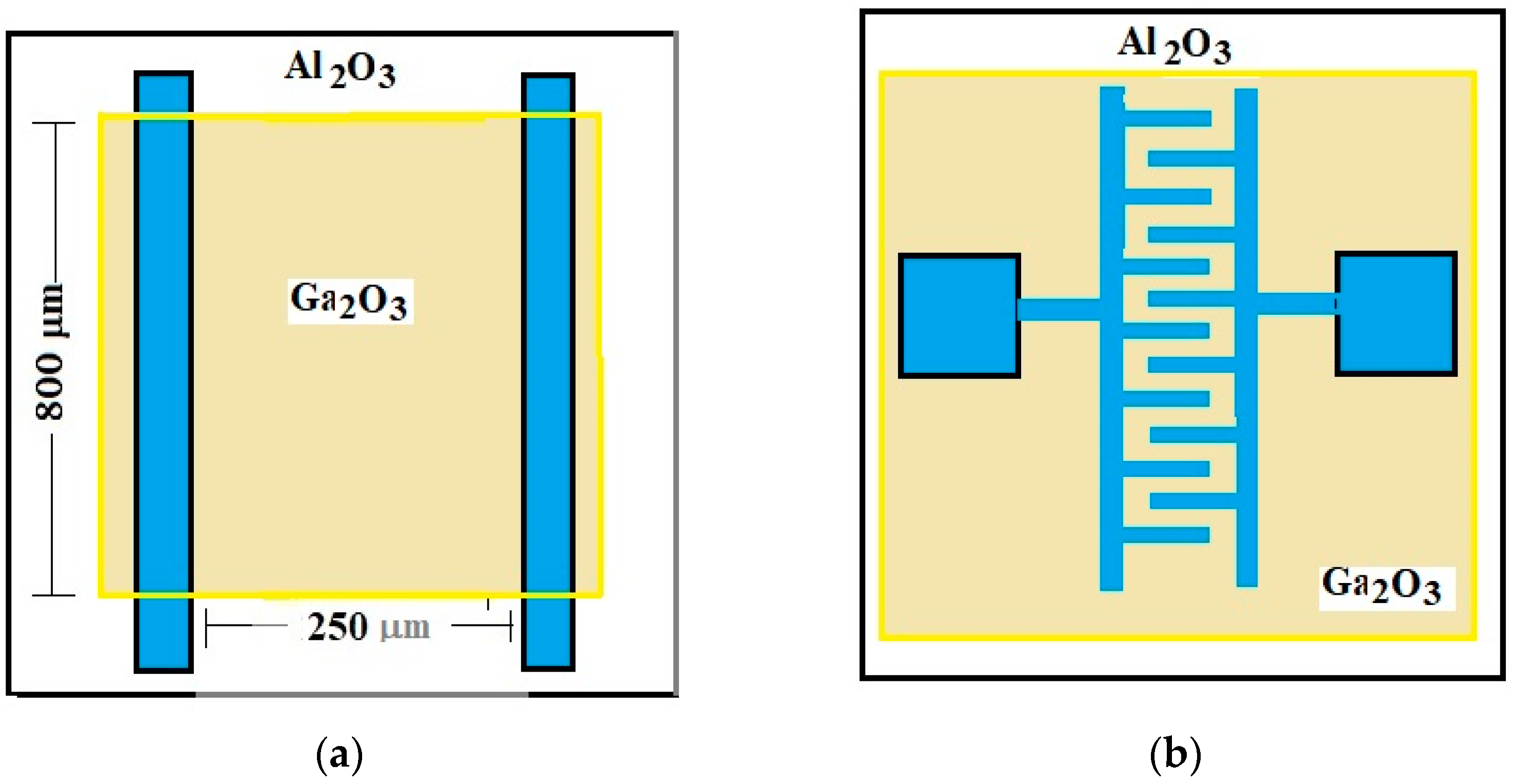
This work considers ultraviolet radiation detectors based on M/β-Ga2O3/M with different interelectrode distances and topologies. The responsivity values of the structures were compared with their response τr and recovery times τd. An analysis of their current–voltage characteristics (I–V characteristics) was carried out over a wide voltage range. For the first time, it was proposed to take into account surface states at the gallium oxide/metal interface which are involved in the capture of free holes.
3. Results
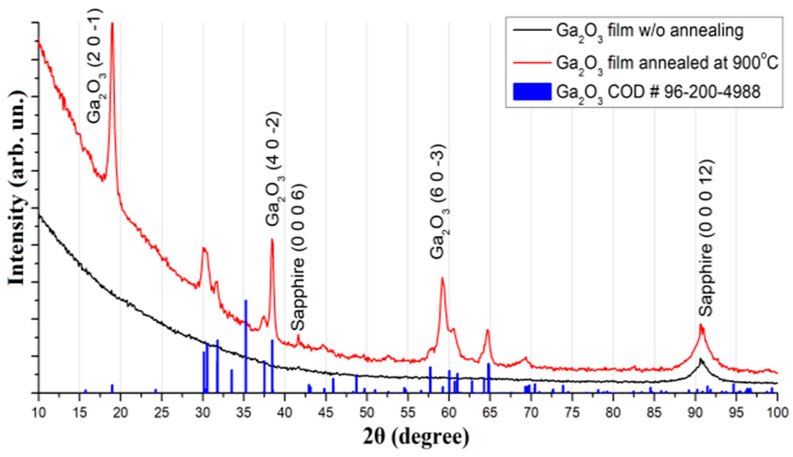
Figure 2 shows the XRD spectra of the gallium oxide film before and after annealing at 900 °C. Peaks at 2θ = 41.7° and 90.7° correspond to (0006) and (00012) crystals planes of sapphire substrates. The gallium oxide thin film without annealing is amorphous (
Figure 2, black line). The film annealed at 900 °C has peaks of the monoclinic β-Ga
2O
3 phase (
Figure 2, red line and blue bars). A partial texture with a preferred orientation of (20-1) Ga
2O
3 planes parallel to the substrate surface is formed in the annealed film.
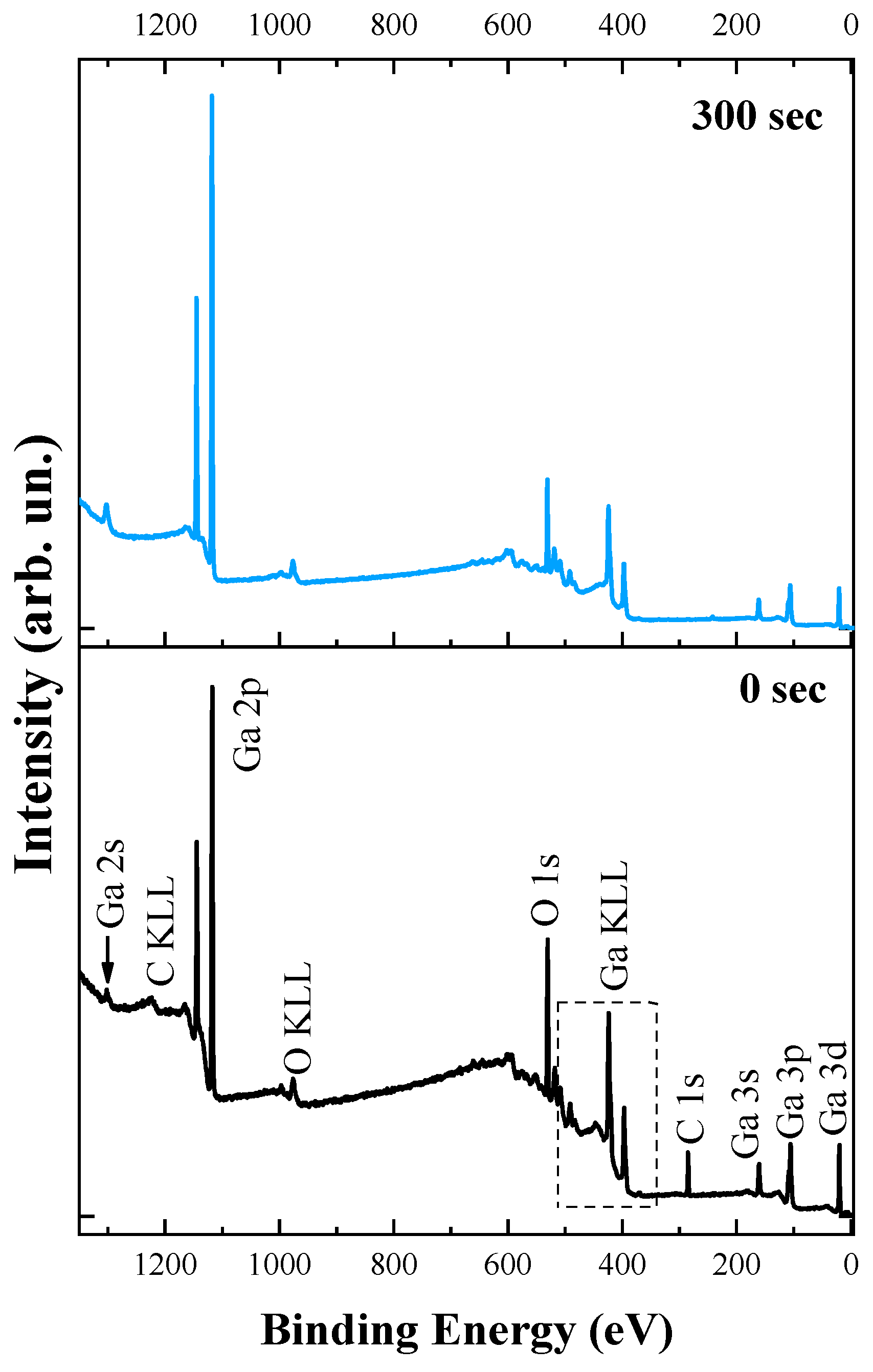
Figure 3 shows the survey spectra of the studied sample before and after 300 s etching with argon ions. In both survey PE spectra, gallium (Ga 2s~1303 eV, Ga 2p~1118.1 eV, Ga LMM~424.5 eV, Ga 3s~161.2 eV, Ga 3p~106.1 eV, and Ga 3d~20.8 eV) and oxygen lines (O KLL~976.5 eV, O 1s~531.4 eV, O 2s~24 eV) are present [
17]. At the same time, the survey spectrum measured from the surface before etching also contains carbon lines (C KLL~1224 eV, C 1s~285 eV). After etching with argon ions, the intensity of the O 1s PE line decreases significantly, and the intensity of the G 2p PE line, on the contrary, increases. This result indicates a change in the [O]/[Ga] ratio. It is important to note that for a more correct quantitative analysis and determination of the [O]/[Ga] ratio, the gallium Ga 3s and the oxygen O 1s lines were used. This is due to the fact that the escape depths of photoelectrons, which are determined by the inelastic mean free path (IMFP) of a photoelectron, for these shells are ~2.2 and ~1.7 nm, respectively, while for the Ga 2p and O 1s shells, the IMFP differs by almost 2 times (see
Table 1). It is clearly seen that the [O]/[Ga] ratio differs before and after ion etching; the reasons for this are outlined in the Discussion section.
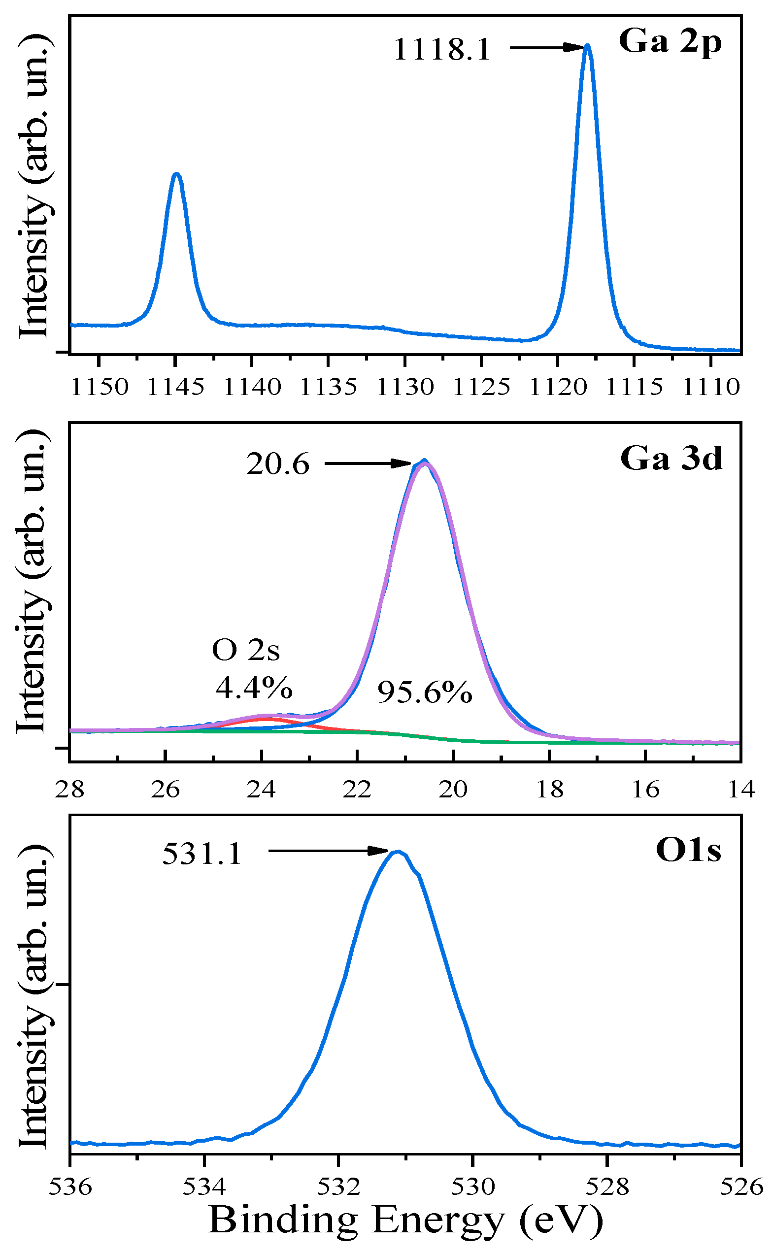
A detailed analysis of the core-level PE spectra measured after 300 s Ar
+ etching showed that the positions of the Ga 2p
3/2, Ga 3d, and O 1s line maxima at the binding energy are 1118.1, 20.6, and 531.1 eV, respectively. This result, together with the [O]/[Ga] ratio, indicates that gallium is in the Ga
2O
3 compound (
Figure 4) [
18].
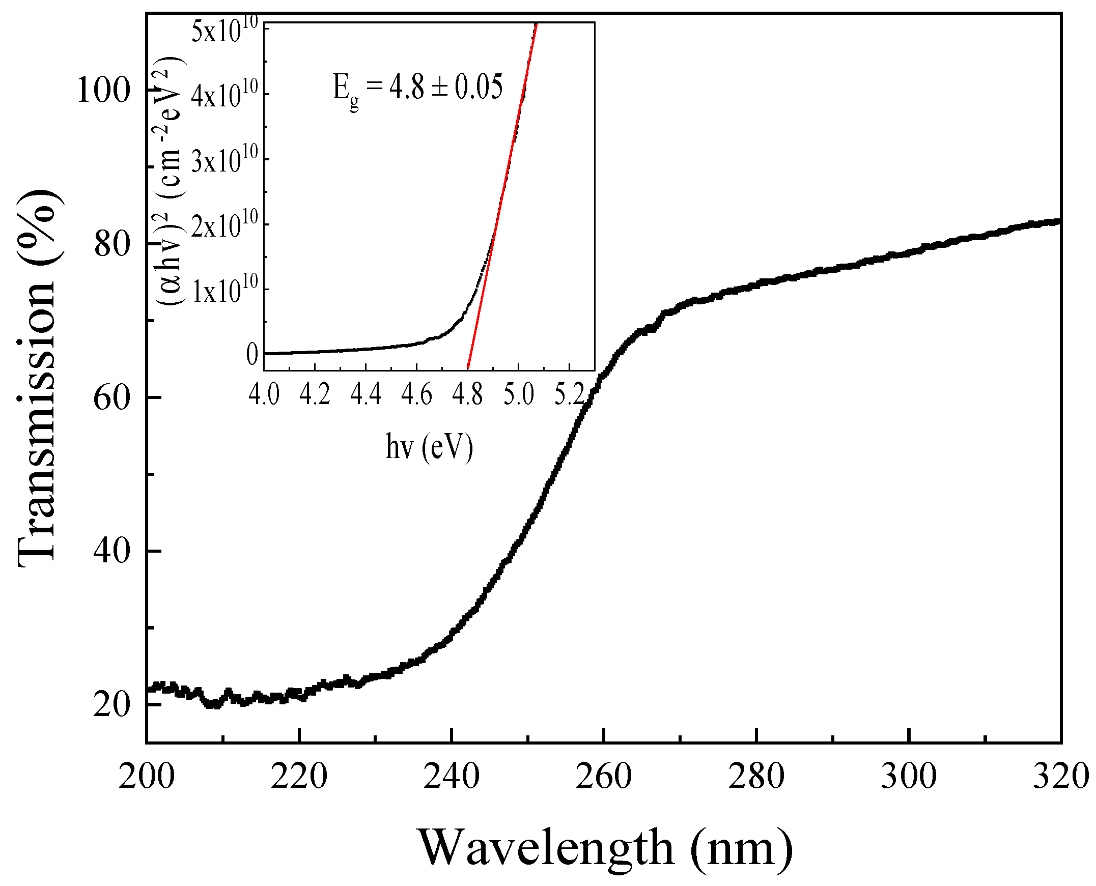
Figure 5 shows the transmission spectrum for β-Ga
2O
3 films. Gallium oxide films are transparent in the near-ultraviolet (UVA) range. The transmittance values T decrease from 83% to 74.5% between wavelengths of 320 nm and 280 nm. The structures are solar-blind. The optical bandgap of the β-Ga
2O
3 film was determined by analyzing the dependence of the absorption coefficient α on photon energy hv, resulting in E
g = 4.8 ± 0.05 eV (
Figure 5, inset).
3.1. Structures of the First Type
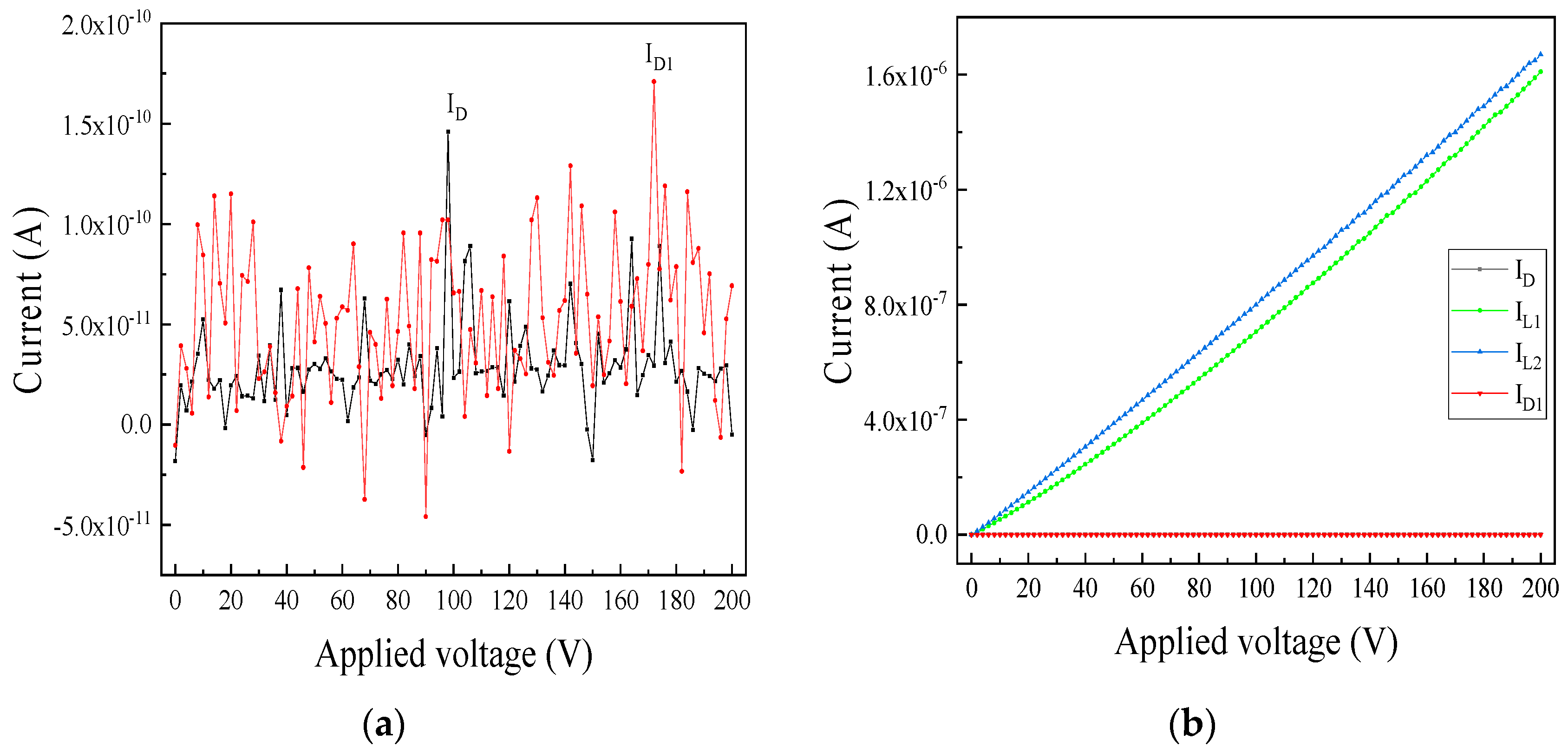
The current–voltage characteristics of both sample types are symmetrical regarding voltage polarity. The dependence of the dark current (I
D) on the voltage (U) is linear for detectors of the first type. I
D values do not exceed 10-180 pA in the voltage range −200 ≤ U ≤ 200 V (
Figure 6a). The current–voltage characteristic maintains a linear shape under UV exposure (
Figure 6b). Ultraviolet radiation with a wavelength of 254 nm leads to an increase in current by 3–4 orders of magnitude. Total current (I
L) values increase linearly under UV exposure to 1.6–1.7 µA with increasing voltage up to ±200 V. In
Figure 6, the I
L1 and I
L2 curves correspond to the currents measured during the first and second measurements of the structures during continuous exposure to UV radiation.
Figure 6a shows that the dark current I
D1 returns to its original values I
D almost immediately after exposure to UV radiation. The dark currents measured before and immediately after turning off the UV light are consistent within experimental error (
Figure 6a). Thus, the structures do not exhibit “persistent conductivity”.
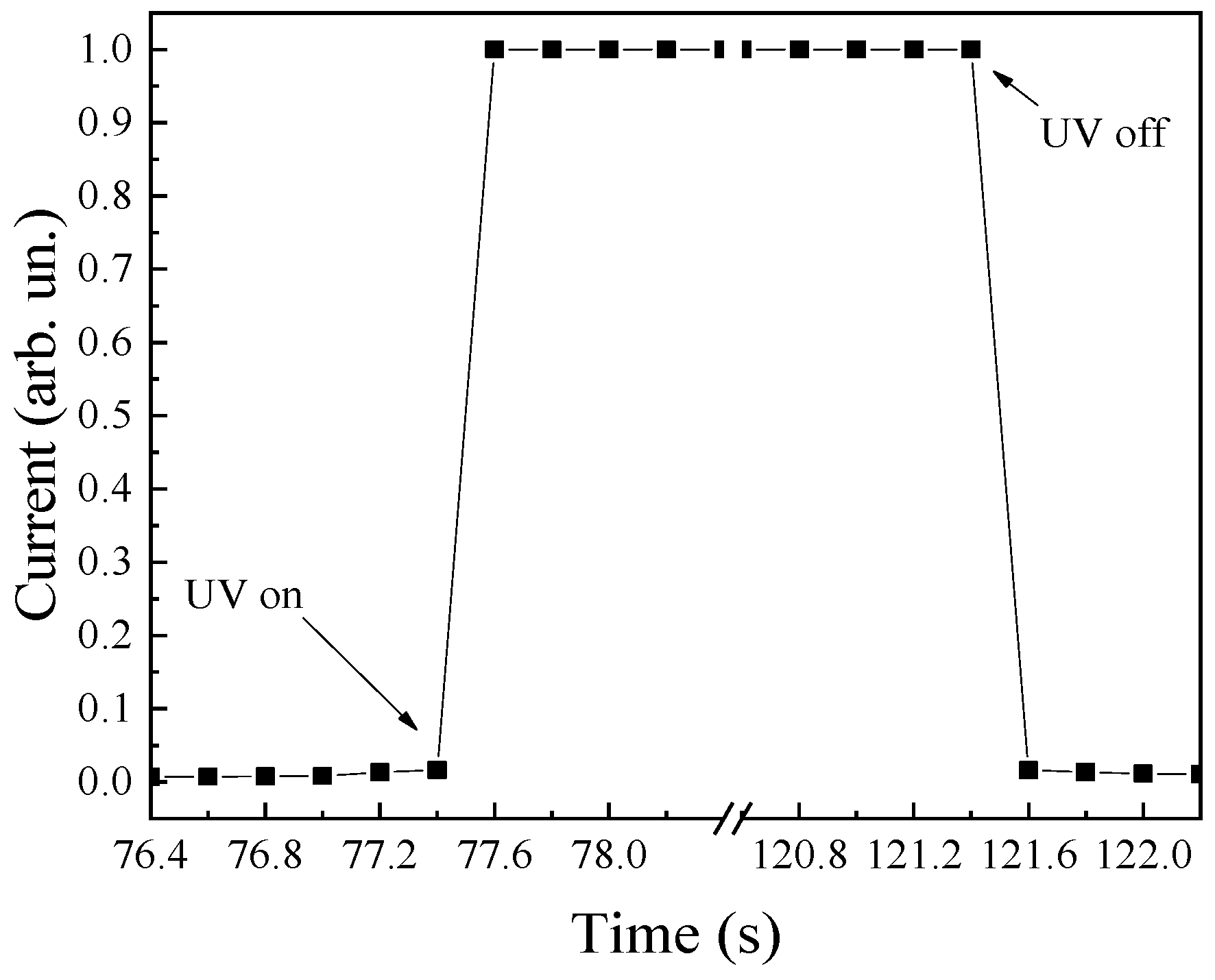
Figure 7 shows the time profile of the current structure under UV exposure with λ = 254 nm. The response times τ
r and recovery times τ
d of the photocurrent are in the millisecond range, confirming the absence of “persistent conductivity” in samples of this type.
3.2. Structures of the Second Type
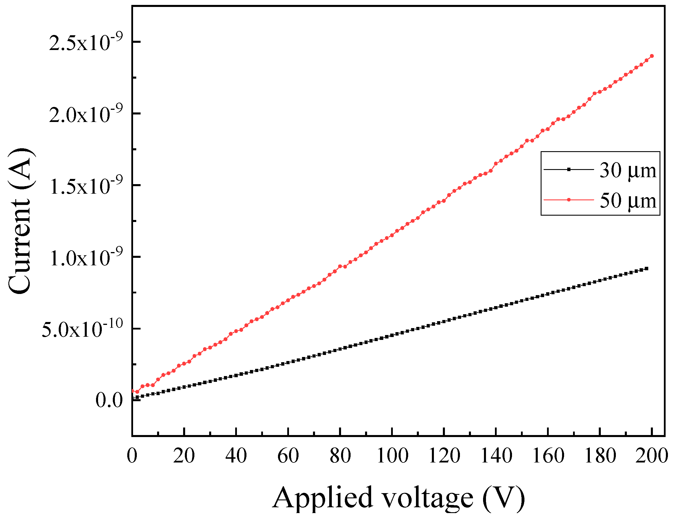
The current–voltage characteristics of structures with interdigitated contacts (structures of the second type) and interelectrode distances of 50 and 30 μm are linear in the range of 0 to 200 V (
Figure 8).
The dark I–V shape changes as the interelectrode distance decreases in structures with interdigitated electrodes. Thus, the dark current–voltage characteristics of the samples with an interelectrode distance of 5 μm and 10 μm cannot be represented by a linear dependence of current I on voltage U in the range of the indicated voltages (
Figure 9, inset).
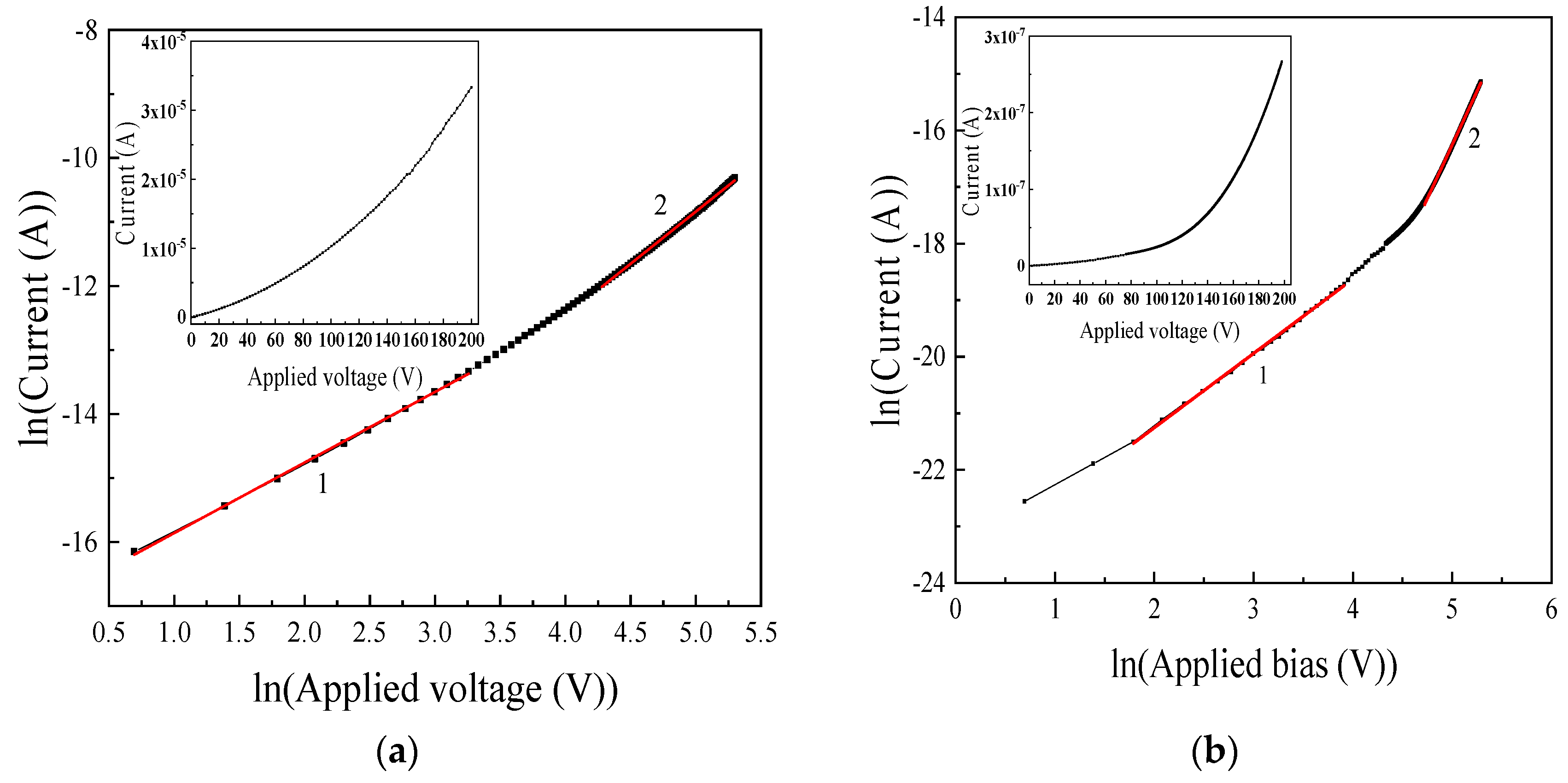
Figure 9 shows the dark current–voltage characteristics on a double logarithmic scale for samples with an interelectrode distance of 5 μm and 10 μm in the voltage range 0 < V ≤ 200 V.
The coordinates ln(I) from ln(U) contain linear sections. The slope of the first section is 1.10 for the structure with an interelectrode distance of 5 μm and 1.63 for the second section. For a structure with an interelectrode distance of 10 μm, the slope of the first section is 1.31, and for the second—3.80. Thus, the dark current–voltage characteristics of samples with interelectrode distances d = 5 and 10 μm can be represented by power law dependence I~U
m, where m = 1 in the range of low voltages and m > 1 at higher electric fields. Thus, the conductivity of structures of the second type in the absence of radiation is determined by space-charge-limited currents (SCLCs) in a semiconductor with traps unevenly distributed in energy (
Figure 9). The relationship between current and voltage in this case is determined by the following expression [
19]:
where N
c is the effective density of quantum states in the conduction band of gallium oxide; ε—the relative permittivity of Ga
2O
3; ε
0—the electrical constant; μ—electron mobility; N
t is the concentration of traps in the Ga
2O
3 film; e—electron charge;
l = m − 1. Exponent
l was determined from the slope of the current–voltage characteristic on a double logarithmic scale. The transition voltage from Ohm’s law to SCLC is described by the following expression:
From experimental data and Expression (2), it was found that the trap concentration N
t was 2 × 10
17 cm
−3 and 6 × 10
17 cm
−3 for structures with d = 5 and 10 μm, respectively. The value of N
t was calculated using
n0 = 1 × 10
17 cm
−3 and N
c = 4 × 10
18 cm
−3 [
20]. The conclusion regarding SCLCs in these samples is consistent with the established concept of multiple traps in the bandgap of β-Ga
2O
3 [
21,
22,
23].
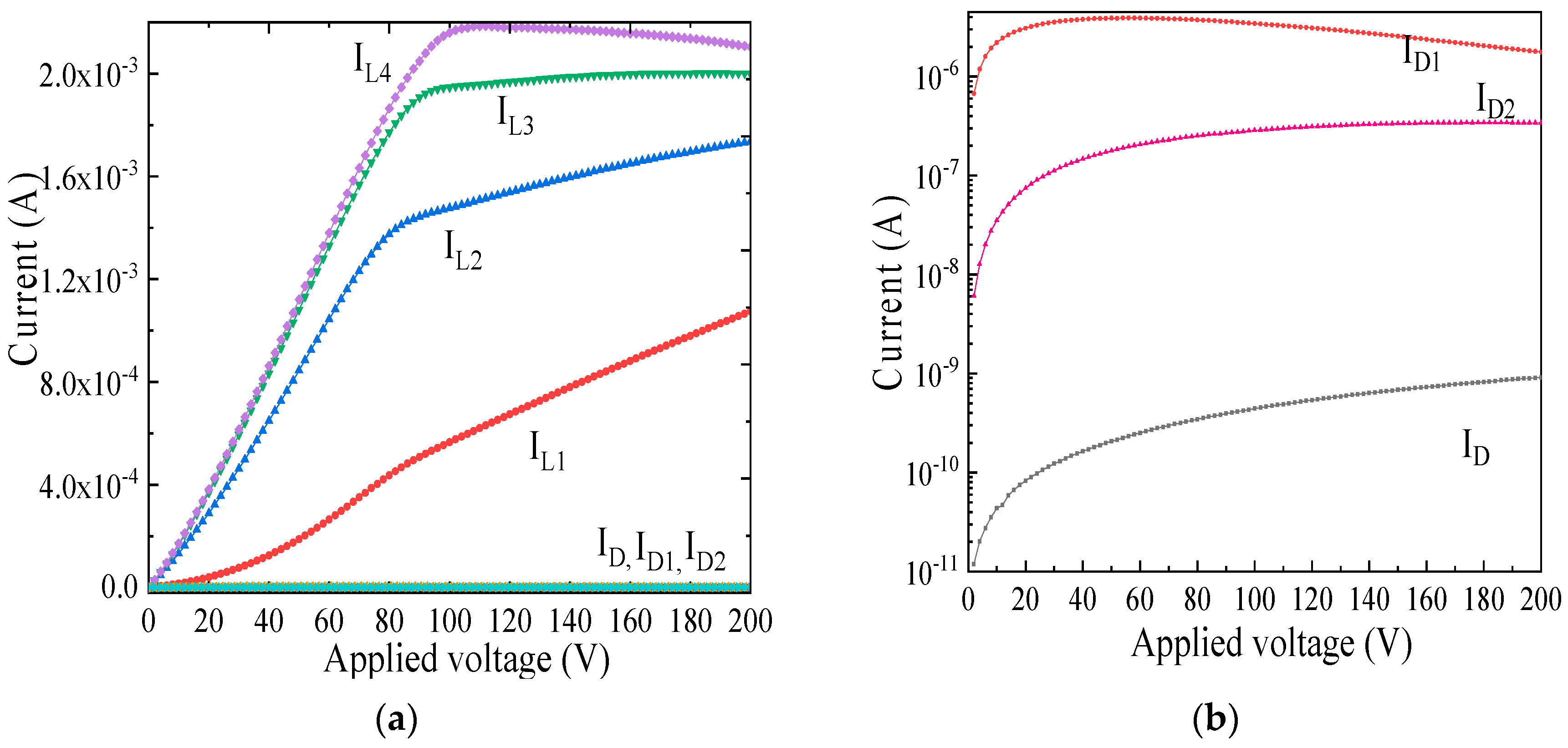
In structures with interdigitated electrodes (structures of the second type), the dependence of current I
L on voltage cannot be represented by a linear dependence, regardless of the interelectrode distance (
Figure 10a).
Initially, I
L increases linearly with increasing voltage, and then a slowdown in the growth of the light current is observed, followed by a decrease, for example, in the
IL4 curve in
Figure 10a.
The light current increases with each subsequent measurement: I
L1 < I
L2 < I
L3 < I
L4 during continuous exposure to radiation with λ = 254 nm (
Figure 10a). Further measurements lead to the stabilization of the light current: it reaches a stationary state.
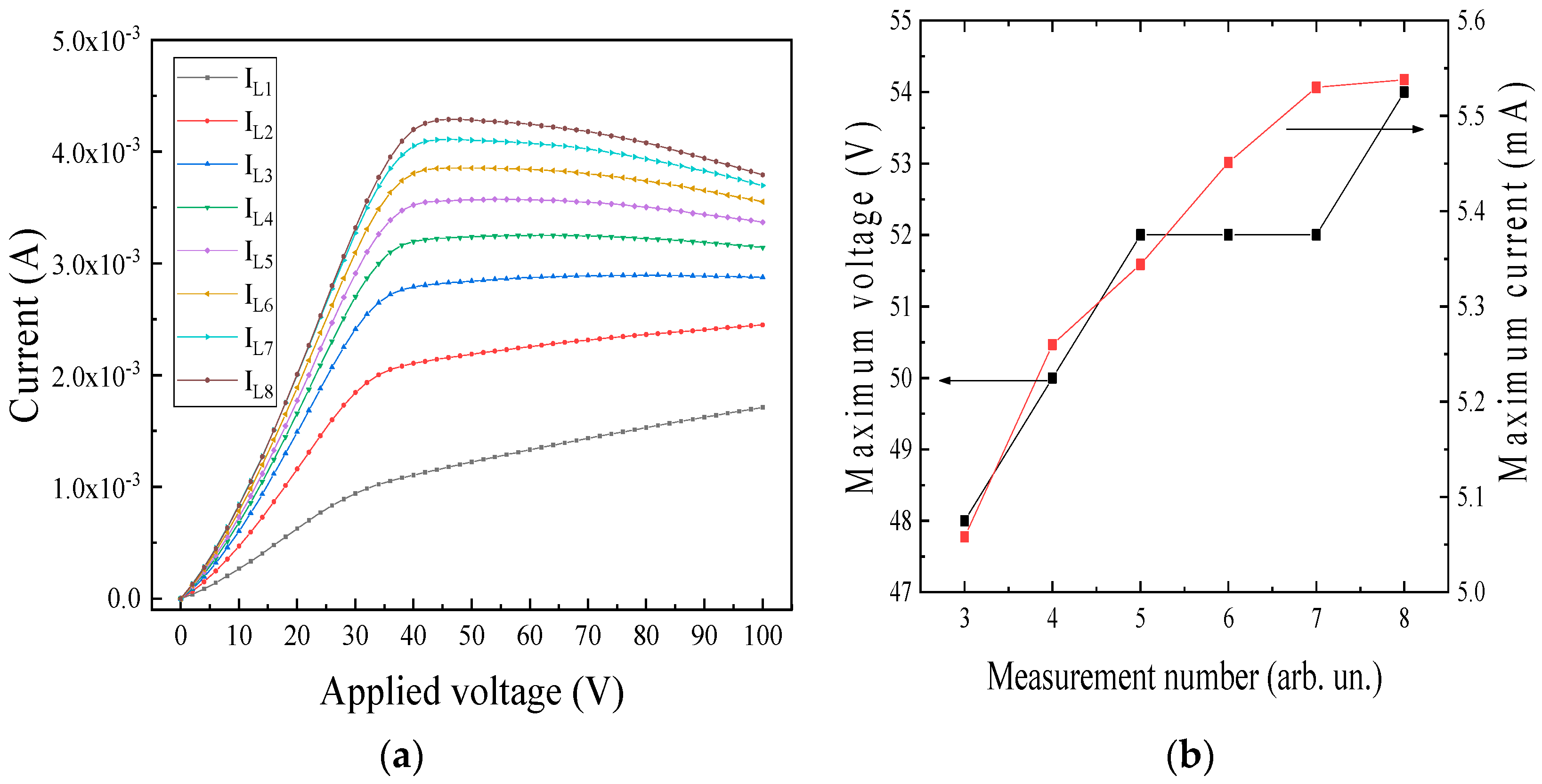
A similar behavior of the current–voltage characteristic under continuous UV exposure is typical for samples with d = 10 μm (
Figure 11a). In the region of strong electric fields, a noticeable decrease in light current is observed with increasing voltage in the structure (
Figure 11a, curves I
L1–I
L8). The maximum points of I
L from U were determined by differentiation (
Figure 11b).
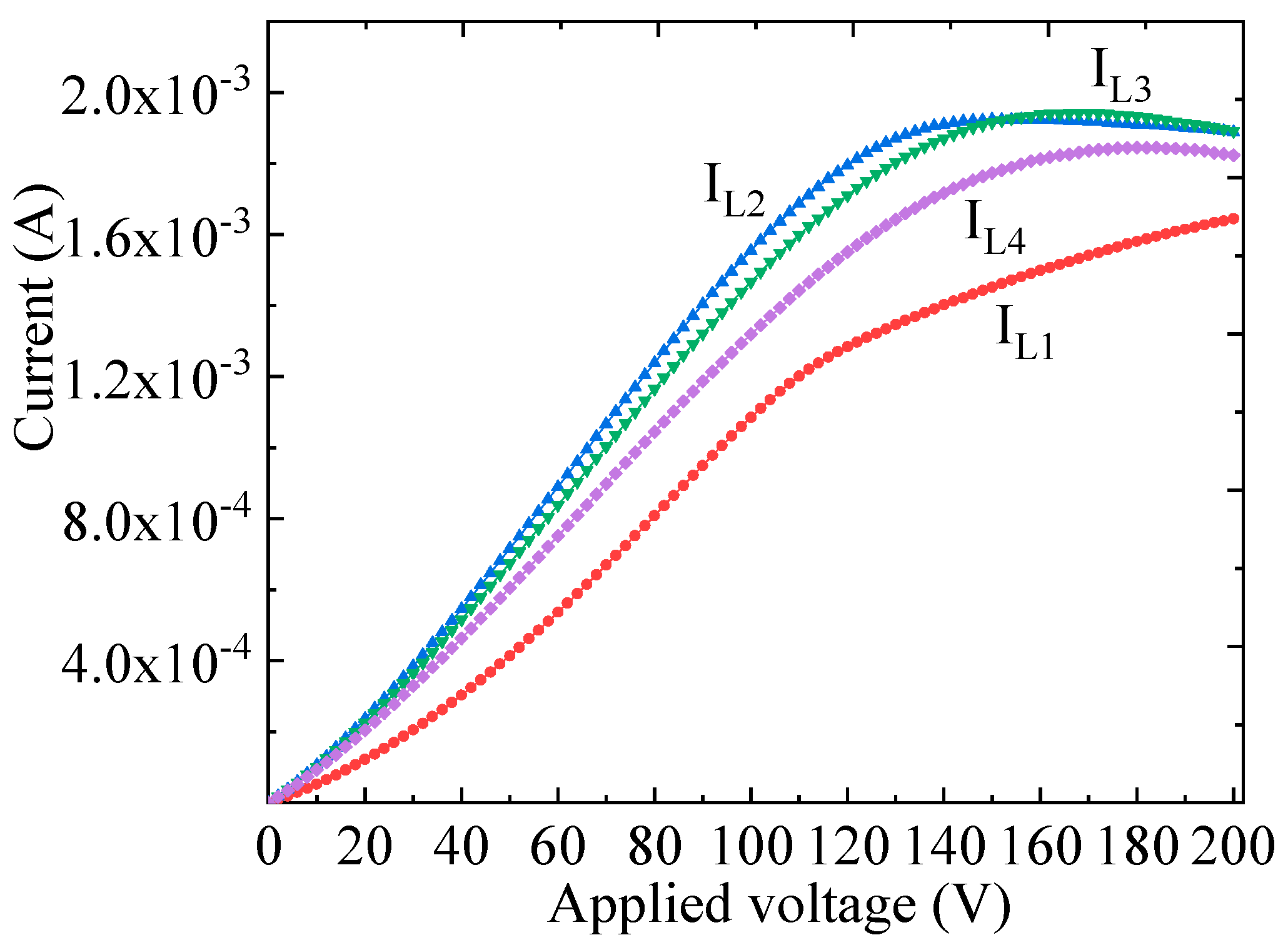
It should be noted that the behavior of the current–voltage characteristic is also affected by radiation with energy hv < E
g. In [
16], the influence of pre-exposure of the structure to radiation with quanta of energy hv less than the bandgap E
g of gallium oxide on the behavior of the current–voltage characteristic is considered. Pre-exposure to broadband radiation increases the photocurrent I
L1 generated by short-wavelength radiation and reduces the deviation of photocurrents I
L2, I
L3, and I
L4 from I
L1 (first measurement) (
Figure 12).
Exposure to radiation with hν < E
g reduces the concentration of active trap centers due to changes in their charge state. This leads to an increase in the photocurrent and stability of detectors in the UV range [
16].
Dark current
ID takes some time to return to its initial value after exposure to UV radiation. In other words, the samples have persistent photoconductivity.
Figure 10b shows dark current–voltage characteristics measured at different times: before UV exposure (I
D); after UV exposure (I
D1); and 30 s after UV exposure (I
D2). The dark current measured immediately after turning off the UV is 3–4 orders of magnitude higher than the initial values of dark current
ID at sample voltages 0 ≤ U ≤ 200 V. The presence of a maximum in the I
D1 curve is explained by the gradual relaxation of the residual current as the voltage across the structure increases.
Thus, characteristics of structures with interdigitated electrodes are a large responsivity value and the presence of “persistent conductivity”.
Table 2 shows the responsivity R and detectivity D* values for structures of the first and second types. The responsivity and detectivity values were calculated using the following expressions [
24]:
where P—light power density,
s—effective area, e—electron charge [
7].
4. Discussions
Based on the XRD and XPS spectra, as well as the dependence of the absorption coefficient α on energy hv, it can be concluded that the film deposited using the RFMS method is β-Ga
2O
3. However, in the XPS data, a significant decrease in the [O]/[Ga] ratio from 1.48 to 1.19 was found after ion beam etching (see
Table 1). This result is not associated with the presence of an oxygen-depleted layer in the Ga
2O
3 film but is explained by the removal of oxygen atoms from the Ga
2O
3 crystal lattice under the influence of argon ions during long-term treatment of the film surface. This effect was previously observed during the etching of various metal oxides with argon ions, as presented in [
25]. Thus, the film obtained in this work is represented by stoichiometric Ga
2O
3 with a low content of oxygen vacancies.
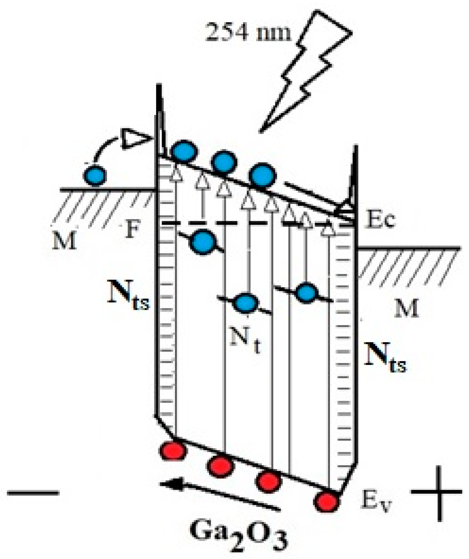
Figure 13 shows the energy diagram of the M/Ga
2O
3/M structure. The energy diagram shown takes into account the ratios of the work function of electrons from metals χ
0 used in our experiments (4.3 eV—Ti, V and 5.7 eV—Pt), and the electron affinity of Ga
2O
3 (4.0 eV) [
26,
27].
The conductivity of structures for both types in the absence of radiation is determined by space-charge-limited currents (SCLCs) in a trap semiconductor. The transition voltage from Ohm’s law to the power law dependence of current on voltage depends on the concentration of traps in the oxide film N
t and is proportional to d
2, as follows from Expression (2). Transition voltage increases with the increasing concentration of free traps (those that have not captured electrons). It is assumed that in structures of the first type with two parallel electrodes, the concentration of free traps is high. Therefore, it is not possible to achieve a transition voltage in the voltage range 0 ≤ U ≤ 200 V. The high concentration of free traps causes low responsivity values R (
Table 2) and relatively short response and recovery times.
It is assumed that structures with interdigitated electrodes have a higher density of surface states (N
ts) at the M/Ga
2O
3 interface, which are divided into fast and slow. The average energy density of surface states should be the same for all samples obtained in one technological cycle. Then, the total number of N
ts is determined by the contact perimeter W. The W values for the studied samples depend on the topology of the contacts and are given in
Table 3. States above the Fermi level are able to trap holes at negative potentials on contact (
Figure 13). Trapped holes do not contribute to recombination. As a result, a high concentration of generated electrons remains in the conduction band, which explains the large responsivity values presented in
Table 3. In addition, the accumulation of holes on the negative electrode leads to the formation of an internal field.
Figure 10a and
Figure 11a demonstrate the significant impact of traps on the response magnitude. The I
L value increases until it reaches a steady-state value with each subsequent measurement. The current–voltage characteristic’s behavior is due to the gradual filling of traps. These traps capture electrons and do not participate in recombination processes during subsequent measurements.
The structures with interdigitated electrodes exhibit a monotonic dependence of current on voltage in the first measurement. However, the shape of the dependence of I
L on U changes with subsequent measurements (
Figure 10a and
Figure 11a). Deviation from the monotonic dependence of light current on voltage occurs at electric fields above a certain critical value E
cr [
28]. The critical field is defined as the electric field strength at which the drift length L
E is equal to twice the hole diffusion length (L
E = 2L
p) [
29].
As the voltage increases, I
L becomes dependent on voltage in the form of a curve with a maximum. The decrease in I
L at voltages exceeding V
max is due to the appearance of an internal electric field E
in, in the opposite direction of the external field E
ex. The voltage V
max, corresponding to the maximum value of the light current, increases with subsequent measurements (
Figure 11b). The effect is explained by an increase in internal field strength E
in with increasing photocurrent, and higher values of E
ex are required to compensate for it. It should be noted that the internal electric field plays a significant role at values of I
L = 10
−4–10
−3 A.
The time dependences of IL(t) are characterized by two processes: fast and slow changes in current. The fast stage of change in IL is determined by processes of generation of electrons from the valence band and excitation of electrons from trap centers located below the Fermi level into the conduction band. The capture of electrons and holes at trap centers occurs simultaneously with the generation process.
Slow processes are caused by recombination (mainly Shockley–Reed–Hall recombination) and capture by traps. The recombination rate Δn/τn depends on the concentration of free holes in the valence band. An increase in the concentration of free holes in the valence band increases the rate of recombination. Thus, the stationary state is established faster, determined by the radiation intensity and the voltage on the structure. In turn, trapped pt holes do not participate in recombination. An increase in pt leads to a decrease in the recombination rate and an increase in the response times τr and recovery times τd. Thus, trapped holes cause high photocurrent values.
It is assumed that free holes are captured not only by defects in the bulk of the gallium oxide film, but also by surface states at the metal/Ga
2O
3 interface.
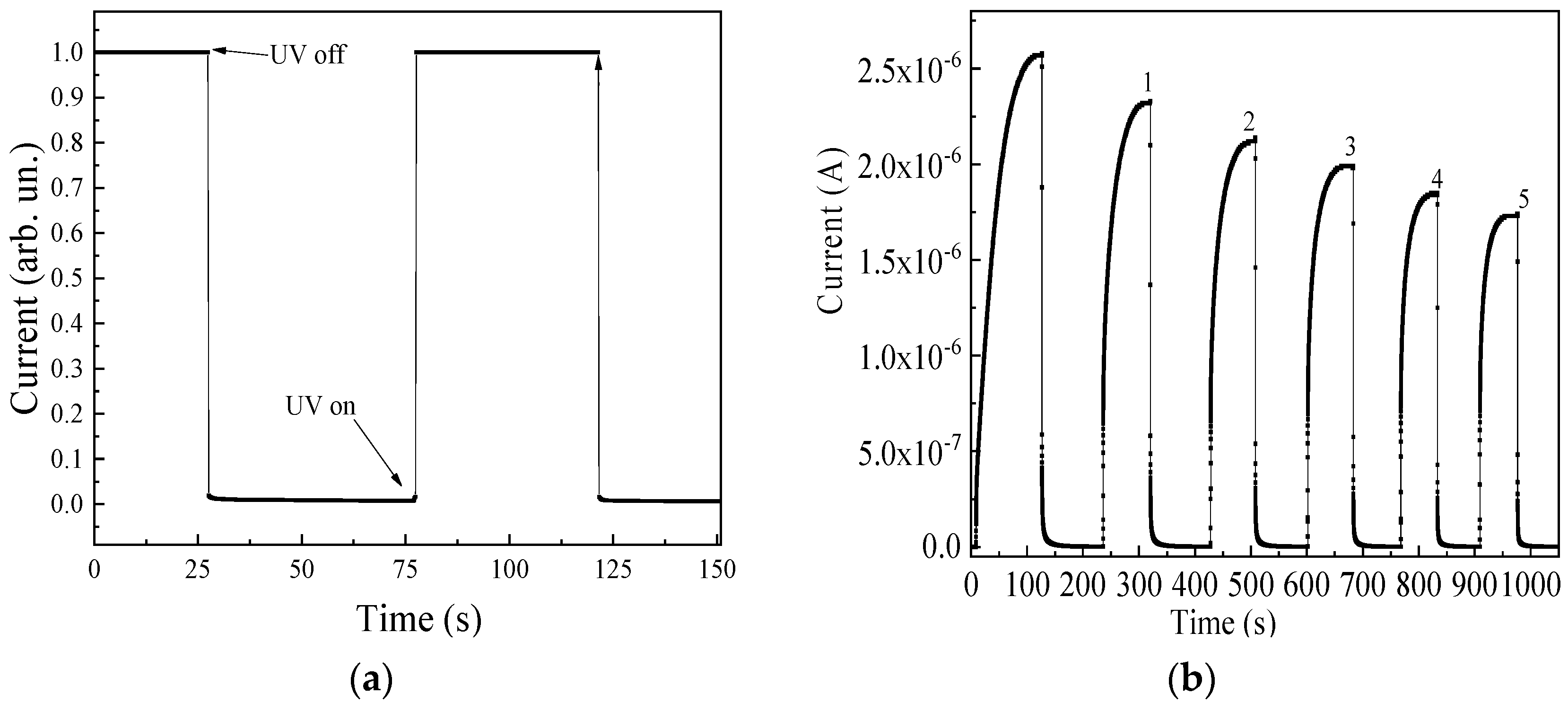
Table 3 shows the response and recovery times for structures with different interelectrode distances. The P parameter determines the perimeter of the contacts used. Times τ
r and τ
d were found as the average value measured for each of the pulses shown in
Figure 14.
The differences in responsivity values and time parameters between structures of the first and second types are explained by the different concentrations of traps that take part in the processes of generation and recombination.
Considering the metal/Ga
2O
3 interface, it is important to take into account the surface states, whose number depends on the perimeter of the contacts W. The
Table 3 shows that the lowest W values were obtained for two-electrode samples. At a low concentration of surface states, a large fraction of the generated holes remain free and are capable of participating in recombination. Thus, there is a low concentration of electrons remaining in the conduction band. Consequently, the response values R (
Table 2) are relatively small, and the values of τ
r and τ
d are fast (
Table 3,
Figure 14a).
Structures with large W values (d = 5 µm) exhibit maximum responsivity R and the longest τ
r and τ
d times (
Table 2 and
Table 3). Increasing the interelectrode distance to 50 µm leads to a fourfold decrease in W. As a result, responsivity is reduced by one order of magnitude, and recovery times are cut in half.
Studies of isotypic and anisotypic Ga
2O
3 semiconductor heterostructures confirm the crucial role of free holes in responding to far-range UV radiation [
31,
32]. The presence of a source of free holes in the valence band of the semiconductor provides a high recombination rate and low values of τ
r compared to similar data for samples with interdigitated electrodes.
5. Conclusions
The electrical and photoelectric characteristics of thin-film M/Ga2O3/M structures with two parallel electrodes (d = 250 μm) and interdigitated contacts with interelectrode distances d = 50, 30, 10, and 5 μm were studied.
The dark currents of the studied structures, regardless of interelectrode distance, were caused by currents limited by the space charge in the semiconductor. Traps were exponentially distributed in the bandgap of gallium oxide. The concentration of trap centers, estimated from experimental data, was (4–6)∙1017 cm−3.
The relationship between the magnitude of responsivity and the time characteristics for structures with different electrode topologies was considered. It was shown that the response and time parameters τr and τd are determined by the concentration of free holes p participating in recombination processes. However, the presence of free holes depends on the concentration of traps that can capture the holes. For the first time, it was proposed to take into account the capture of holes by the surface states of Nts at the metal/Ga2O3 interface in addition to their capture by trap centers in the bulk of the oxide film. The concentration of Nts depends on the topology of the electrodes, in other words, on the perimeter.


 ,
, 


