Article

The Synthesis and Characterization of CdS Nanostructures Using a SiO2/Si Ion-Track Template

by
Aiman Akylbekova
1,
Kyzdarkhan Mantiyeva
1,
Alma Dauletbekova
1,
Abdirash Akilbekov
1,
Zein Baimukhanov
1,*,
Liudmila Vlasukova
2,
Gulnara Aralbayeva
1,*,
Ainash Abdrakhmetova
1,
Assyl-Dastan Bazarbek
1 and
Fariza Abdihalikova
1
1
Faculty of Physics and Technology, L.N. Gumilyov Eurasian National University, 2 Satbaev Str., Astana 010008, Kazakhstan
2
Faculty of Radiophysics and Computer Technologies, Belarusian State University, Kurchatov Street 5, 220045 Minsk, Belarus
*
Authors to whom correspondence should be addressed.
Crystals 2024, 14(12), 1091; https://doi.org/10.3390/cryst14121091
Submission received: 19 October 2024 / Revised: 5 December 2024 / Accepted: 15 December 2024 / Published: 19 December 2024
(This article belongs to the Section Inorganic Crystalline Materials)

Abstract

:
In the present work, we present the process of preparing CdS nanostructures based on templating synthesis using chemical deposition (CD) on a SiO2/Si substrate. A 0.7 μm thick silicon dioxide film was thermally prepared on the surface of an n-type conduction Si wafer, followed by the creation of latent ion tracks on the film by irradiating them with swift heavy Xe ions with an energy of 231 MeV and a fluence of 108 cm−2. As a result of etching in hydrofluoric acid solution (4%), pores in the form of truncated cones with different diameters were formed. The filling of the nanopores with cadmium sulfide was carried out via templated synthesis using CD methods on a SiO2 nanopores/Si substrate for 20–40 min. After CdS synthesis, the surfaces of nanoporous SiO2 nanopores/Si were examined using a scanning electron microscope to determine the pore sizes and the degree of pore filling. The crystal structure of the filled silica nanopores was investigated using X-ray diffraction, which showed CdS nanocrystals with an orthorhombic structure with symmetry group 59 Pmmn observed at 2θ angles of 61. 48° and 69.25°. Photoluminescence spectra were recorded at room temperature in the spectral range of 300–800 nm at an excitation wavelength of 240 nm, where emission bands centered around 2.53 eV, 2.45 eV, and 2.37 eV were detected. The study of the CVCs showed that, with increasing forward bias voltage, there was a significant increase in the forward current in the samples with a high degree of occupancy of CdS nanoparticles, which showed the one-way electronic conductivity of CdS/SiO2/Si nanostructures. For the first time, CdS nanostructures with orthorhombic crystal structure were obtained using track templating synthesis, and the density of electronic states was modeled using quantum–chemical calculations. Comparative analysis of experimental and calculated data of nanostructure parameters showed good agreement and are confirmed by the results of other authors.

1. Introduction

Inorganic composite materials in the nanoscale region have unique electrical and optical properties that make them suitable for versatile applications. Semiconductor thin films have great potential for environmental and energy applications due to their unique characteristics [1,2,3,4].
Cadmium sulfide films are an important and promising semiconductor material used in many technological and industrial applications due to their excellent optical and electrical properties [5]. In addition, CdS is also of considerable interest due to its use in the fabrication of heterojunction solar cells and other optoelectronic devices. In particular, CdS has significant applications in several fields, such as photocatalysis [6], lasers [7,8], light-emitting diodes, and field-effect transistors [9].
In nanotechnological applications, SiO2/Si track templates are of great interest. Nanoporous SiO2/Si layers can be created using irradiation with fast heavy ions followed by the selective etching of silicon dioxide. In [10,11,12,13], the process of irradiation and the formation of nanopores in thermally oxidized SiO2/Si silicon wafers was studied. It was found that, upon applying irradiation with subsequent etching with hydrofluoric acid (HF) in SiO2 layers, nanopores were formed, which provide fast local deposition at low temperatures (and an easily controlled density with sizes ranging from 10 nm to several micrometers).
Recently, semiconductor photocatalysis technology, among the various kinds of photocatalytic systems, has attracted wide attention. CdS is one of the most interesting semiconductor materials because of its narrow bandgap (~2.4 eV) and the corresponding position of the zone structure [14,15]. By integrating a freestanding CdS nanowire into a silicon nitride photonic chip, the authors of [16] created a highly compact single-mode CdS nanowire laser. Moreover, the authors of [17] successfully prepared BiVO4/CdS composites using a two-step ultrasonic precipitation method, which improved the high separation efficiency of photoinduced charge carriers and enhanced the catalytic efficiency of RhB degradation. In [18], CdS nanowires were prepared using a hydrothermal method, and BiOBr/CdS composites with different mass ratios were also successfully prepared using a simple two-step sonication/deposition method employing CdS nanowires as a deposition template. Several researchers showed that the efficiency of many solar cells strongly depends on the property of the CdS buffer layer and that the chemical deposition (CD) method is the most convenient way to deposit these layers [19]. Additionally, in [20], a CdS nanomaterial doped with Pr+3 and Nd+3 was obtained. The ions were synthesized at room temperature using a simple chemical precipitation method. The synthesized sample was characterized using powder X-ray diffraction (XRD), scanning electron microscopy, transmission electron microscopy, and energy-dispersive X-ray spectroscopy. The authors of [21] synthesized CdS nanoparticles doped with Mn via CD using different concentrations of Mn in Cd1−xMnxS.
In [17,18,21], methods of obtaining nanomaterials were developed using two-cycle deposition, which requires a long time period and great effort; to address these problems, we considered obtaining CdS nanostructures in a track template SiO2 nanopores/Si using CD, which allows us to obtain CdS nanocrystals in a relatively short time and at low temperatures. This method also makes it possible to control the density of nanopores with sizes ranging from 10 nm to several micrometers.
After CD, SEM images were acquired for the samples using a Zeiss Crossbeam 540 scanning microscope (Carl Zeiss AG, Oberkochen, Germany) at Nazarbayev University, and the morphology of the structural CdS features was investigated using a Rigaku Smartlab SE diffractometer (Rigaku Corporation, Tokyo, Japan), also at Nazarbayev University and Raman spectroscopy was performed using a Solver Spectrum spectrometer from NT-MDT (NT-MDT, Zelenograd, Russia) at Al-Farabi Kazakh National University. In this study, we report on the structural, morphological, optical, and electrical properties of CdS nanocrystals.

2. Materials and Methods

The CdS nanostructures used in this study were grown via CD on a SiO2 nanopores/Si substrate. A ~700 nm thick silicon dioxide film was thermally grown on an n-Si (100) wafer. Latent ion tracks in the SiO2 layer were created by irradiating them with 231 MeV swift heavy Xe ions to a fluence of 108 cm−2. SiO2/Si samples of 5 × 5 mm and 20 × 20 mm were cut from an oxidized Si wafer. Etching latent tracks in a 4% hydrofluoric acid solution for 5–10 min resulted in the formation of stochastically distributed pores in the form of truncated cones with different diameters.
SiO2 nanopores were filled with cadmium sulfide using templated synthesis via CD methods on the SiO2 nanopore/Si substrate. The solution contained 3.66 g of cadmium chloride and 0.26 g per 100 mL of distilled water of ammonium chloride. The nanopores were then heated at 45 °C until they became clear. A total of 38 mL of ammonia was added dropwise to maintain the pH at 9. The formation of CdS started after the addition of 0.38 g of thiourea, and the color of the solution changed from transparent to orange while the temperature of the solution was already brought to 75 °C, as in [22]. The deposition time varied from 20 to 40 min. In chemical bath deposition, ammonia is a complexing agent that controls the release of metal (Cd2+) and sulfur (S2−) in an alkaline solution [23,24].
The surface morphology of nanoporous SiO2/Si before and after CdS synthesis was investigated using a Zeiss Crossbeam 540 scanning electron microscope (SEM). The crystal structure of the filled silica nanopores was investigated using XRD on a Rigaku SmartLab diffractometer (Tokyo, Japan). The measurements were carried out at room temperature in the range of 2θ angles from 40° to 70° in the scanning mode with a step of 0.01°. The measurement of the lattice period value and the refinement of structural parameters were performed using the TOPAS 4.2 program and the international ICDD database (PDF-2 Release 2020 RDB).
Photoluminescence (PL) spectra were recorded at room temperature using a CM 2203 spectrofluorometer (SOLAR, Minsk, Belarus) in the spectral range from 300 to 800 nm under excitation at a wavelength of 240 nm at L.N. Gumilyov Eurasian National University.
The CVCs for different deposition times of CdS/SiO2/Si were measured using an HP 66312A current source and an Agilent 34401A multimeter (Santa Clara, CA, USA). Current volt–ampere characteristics (CVCs) were measured from a 400 mm2 array of filled nanopores. The setup for measuring the CVCs is as follows: The nanopore-filled sample was placed between two conductive metal electrodes so that the electrodes overlapped only at the nanopore locations. The electrodes were then connected to a constant voltage source with a series connection of a multimeter.

3. Results

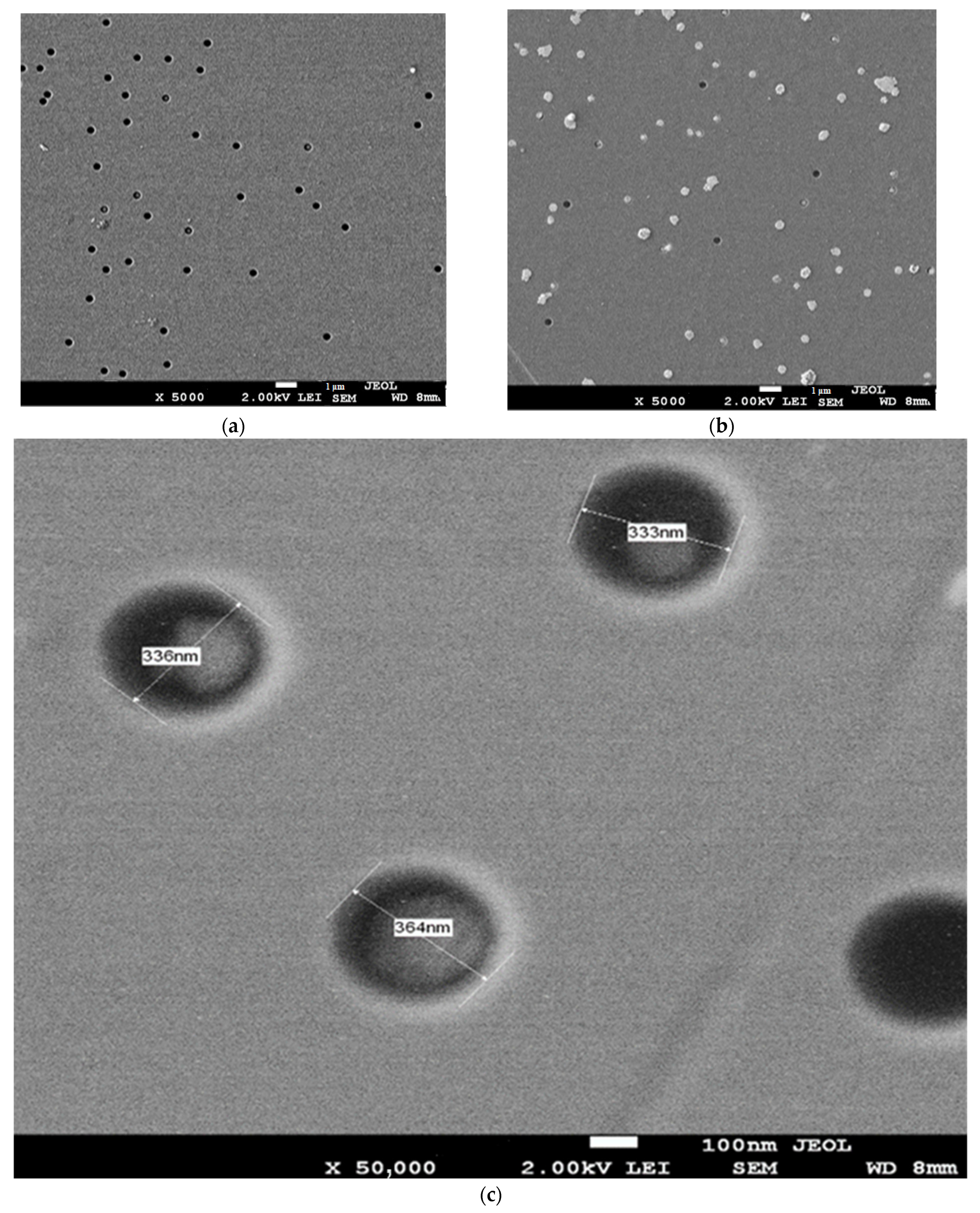
3.1. Surface Morphology

To characterize the size and surface shape of silicon nanopores (SiO2) before and after filling, we used a double-beam SEM. It should be noted that the degree of nanopore filling depends on the deposition time and the temperature of the chemical solution.
Thus, to achieve the highest degree of nanopore filling, the deposition process was carried out for between 20 and 40 min at the deposition temperatures of 50 °C and 75 °C. It is important to note that a slightly alkaline environment (pH) should be created for complete deposition. The results of the surface morphological study of the deposited CdS nanostructures are shown in Figure 1b,c. The SEM image of the sample before CD (Figure 1a) shows that the pores are well defined, spherical in shape, and uniform in size, and the surface density of the nanopores is 108 cm−2. Figure 1b shows the SEM image of the surface of silica nanopores at a 75 °C solution temperature after 30 min of CD, in which the filling degree was approximately 85% and the average diameter of the nanopores was 364 nm.
The structural properties of the synthesized CdS nanostructures were studied using XRD analysis. The structural identification of the CdS nanostructures was carried out using XRD in the range of 2θ angles from 40° to 70°.
The XRD results showed the formation of CdS nanocrystals with an orthorhombic crystal structure and space group 59 Pmmn (Figure 2 and Table 1). Peaks at 2θ of 61.48° and 69.25° were observed for all samples (Graphs 1, 3). The intensity of the observed peak strongly depends on the amount of deposition time. Also, the analytical results showed that the CdO phase with cubic structure was formed in the crystal in a small quantity during the synthesis process (Graph 2). This phase is considered by the authors [25,26] as the phase of impurities.
It is well known that CdS is a Raman-active nanomaterial. The Raman scattering of CdS nanostructures was observed in the backscattering configuration and analyzed using a Solver Spectrum spectrometer from NT-MDT at room temperature. Figure 3 shows the Raman light scattering spectrum of the CdS nanostructures; this spectrum is dominated by the progression in the longitudinal optical (LO) phonon mode. Two LO phonon peaks of CdS were observed: the first, stronger peak is the longitudinal optical mode (LO1) at 301 cm−1; the other, weaker one is the LO mode overtone (LO2) at 600 cm−1, which agrees with the well-known results of past studies. The mode peak surface of small 1 µm CdS crystallites at 296 cm−1 and its second-order peak at 592 cm−1 were observed, which agrees with the fact that one of the striking features of the Raman spectra of CdS is a remarkable series of longitudinal optical phonon overtones [25]. The peak corresponding to the first-order optical background mode (LO1) is intrinsic to the hexagonal (wurtzite) modification of CdS, and the peak at 600 cm−1, corresponding to the second-order optical background mode of CdS (LO2), corresponds to the cubic (sphalerite) modification of CdS.
In addition to experiments, computer calculations of pure CdS crystals were also carried out. To describe the exchange-correlation energy of the electronic subsystem, a functional in the generalized gradient approximation (GGA) and the periodic supercell model was used. The calculations were performed using CRYSTAL 17 software [26]. Figure 4a,b shows a complete zone energy diagram of the CdS nanostructures along the highly symmetric lines of the tetragonal Brillouin zone, together with the density of electronic states. The valence band maximum appeared near the G point, while the conduction band minimum appeared at the T point. In [27,28], it is stated that the smallest energy gap of the forbidden zone is localized in the center of the Brillouin zone (G point). This means that the crystal is characterized by a direct forbidden zone. The calculated width of the forbidden zone for the CdS nanostructures was 2.39 eV, which agrees well with the results in [29].
CdS is also halite, a rock salt structured and crystallized in the orthorhombic space group Pmmn. Cd2+ is bonded to six equivalent S2 atoms, forming a mixture of CdS octahedra with common edges and angles.
There are two shorter (2.75 Å) and four longer (2.76 Å) Cd–S bond lengths. S2− is bonded to six equivalent Cd2+ atoms, forming a mixture of CdS octahedra with common edges and angles that range from 0 to 2°. The calculated values of lattice constants are presented in Table 2, and they are in good agreement with the experimental observations (Table 1).

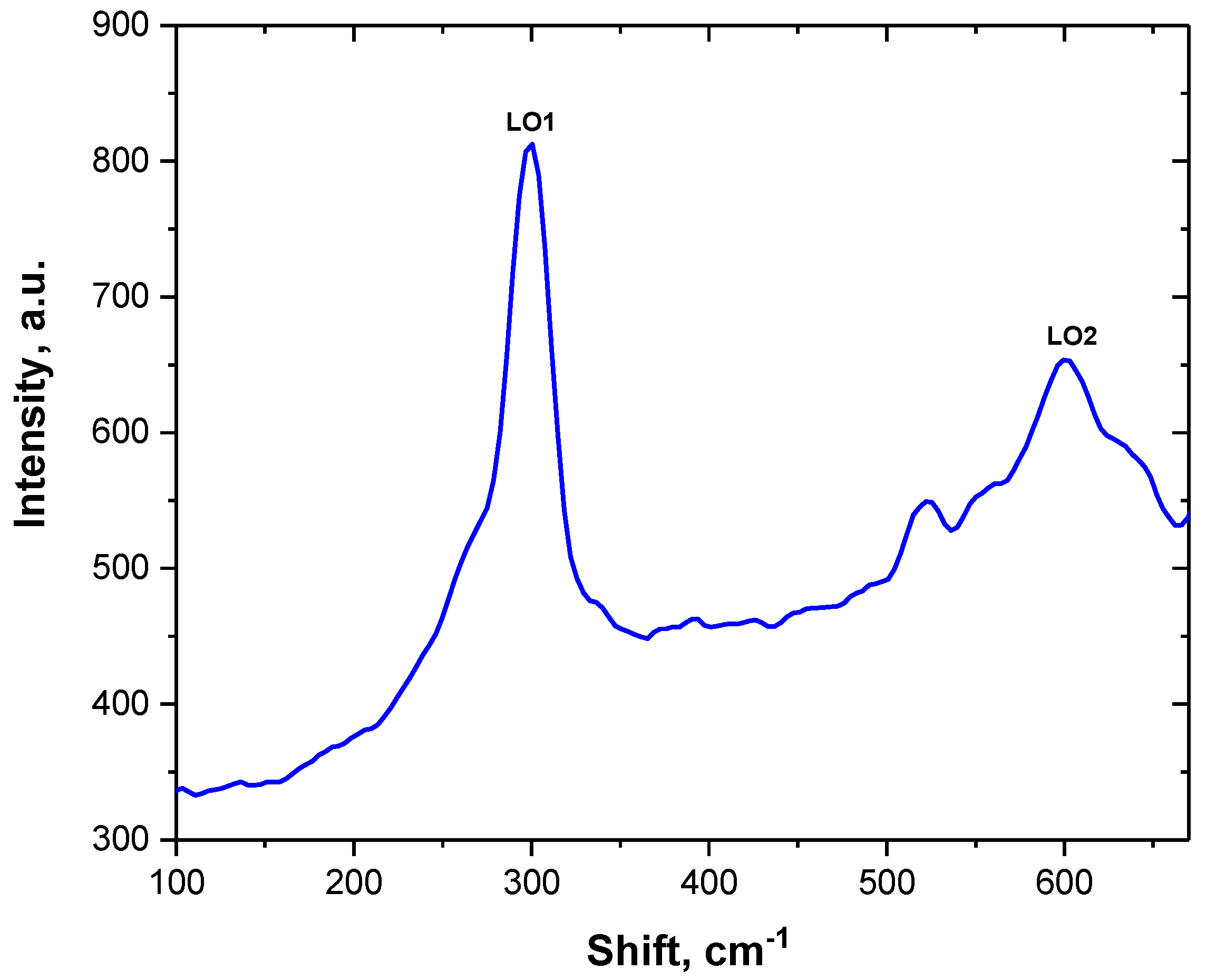
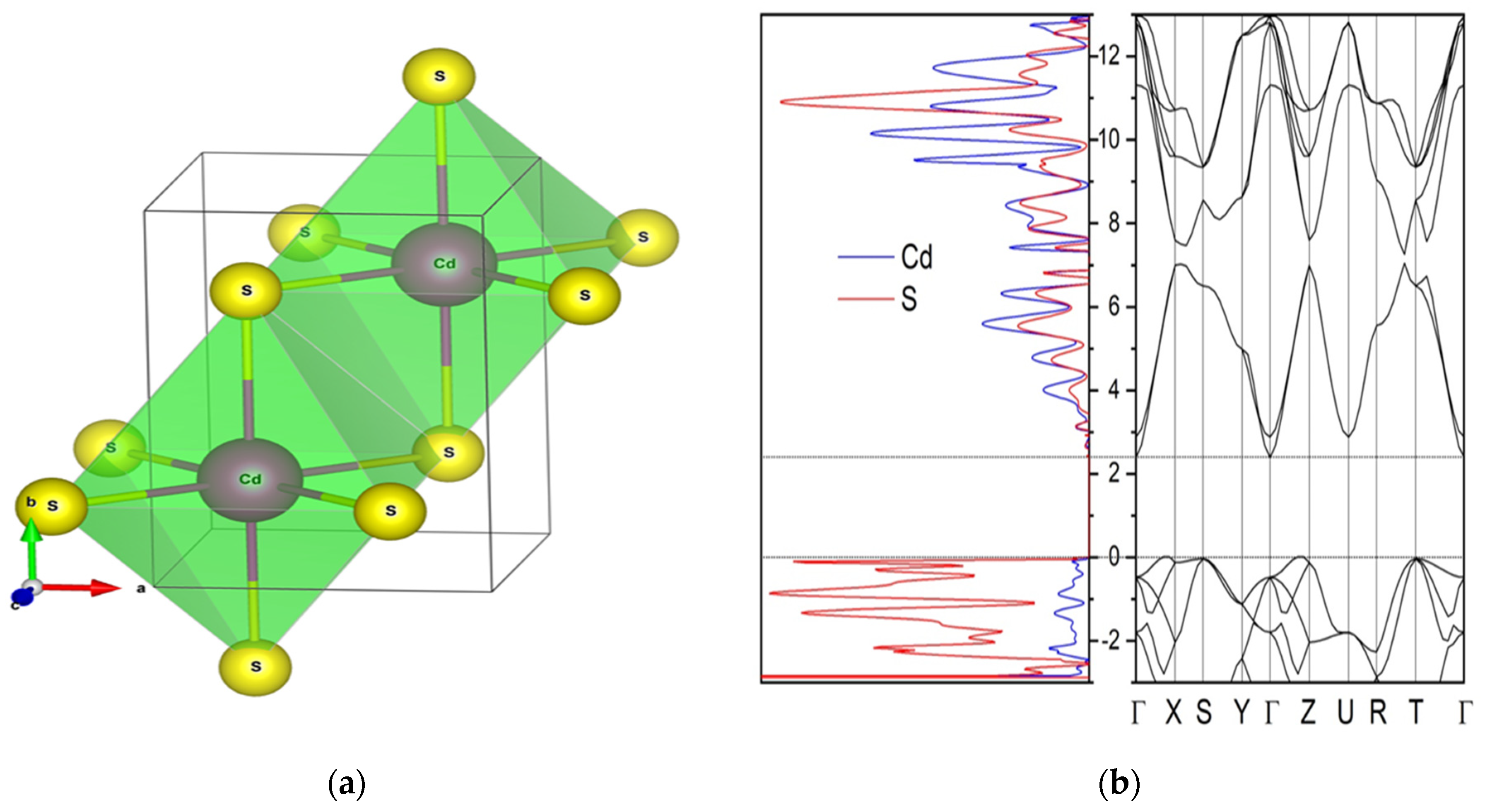
3.2. Optical Properties and CVCs of CdS/SiO2/Si Nanocrystals

Optical studies were carried out by measuring the PL of CdS nanostructures deposited in SiO2 nanopores/Si on a CM2203 spectrofluorometer (SOLAR) in the spectral range from 300 to 800 nm at an excitation wavelength of 240 nm. Several visible light lines were observed in the FL spectra of the CdS nanostructures (Figure 5). The decomposition of the complex experimental FL spectrum into several independent Gaussians was performed using the Origin software package. The nanostructures have a blue band at 2.53 eV and green bands at 2.37 eV and 2.45 eV. Generally, two types of emission, exciton emission, and trap luminescence, are observed from semiconductor nanoparticles, as in [30,31]. Exciton emission is located near the absorption edge of CdS particles and usually has two emission bands, including a green band around 2.37 eV (522 nm), which agrees well with our data [30,32]. High-aspect-ratio CdS nanocrystals have many surface and subsurface defects, such as grain boundaries and sulfur/cadmium-related defects. These defects influence the PL properties of CdS nanocrystals [29,30].
In Figure 5, the peak at 2.37 eV (522 nm) shows weak and sharp emissions. The weak emission band at shorter wavelengths is explained by the direct transition from the conduction zone to the valence zone [33]. This indicates a sufficiently high degree of crystallinity of the particles. The main luminescence band is broad and is attributed to CdS emission by trap emission. The peak at energy 2.45 eV belongs to the “green” interval of the visible spectrum. If the crystal is grown in excess sulfur, only a weak series with a head line at 2.45 eV is observed. In [29], the peaks corresponding to 2.37 eV and 2.45 eV were attributed to the transition of sulfur vacancy (VS) into the valence zone and the recombination of donor/acceptor pairs. The peak at 2.53 eV (490 nm) is responsible for exciton scattering, as in [34] (Table 3).
In this study, the silicon substrate for growing nanostructures in nanopores SiO2 has n-type conductivity. It is known that, for a direct current to appear, the magnitude of the potential barrier must be reduced. For this purpose, it is necessary to apply a direct voltage close to the value of the contact potential difference to the p–n junction φ к in a silicon-based p–n junction φ к = ( 0.6 ÷ 0.8 ) , as in [35]. From the graph shown in Figure 6 (curve 4), the forward voltage exceeds the value of the potential barrier ( U > φ к ) in the junction, drops to almost zero and then becomes quasi-linear ohmic (CVCs) (curve 4 in Figure 6). Thus, as the forward bias increases (U > 0), a significant increase in forward current is observed (Figure 6 curves 2, 3, 4). It can be seen from the graph that the fourth sample (curve 4) has better conductivity than the rest (curves 2, 3), and this is probably because the template is filled with CdS nanoparticles well (Figure 1b). Additionally, at reverse bias (U < 0), a slight increase in leakage current is observed, which is probably due to the lower contact efficiency between the CdS nanostructures and the SiO2 layer than that between the Si layer and SiO2 layer. It is important to note that the leakage current is negligible in the current p-junction fabrication technology. According to the results of CVC analysis, the CdS/SiO2/Si nanostructures have one-sided electronic conductivity.

4. Conclusions

In this study, CdS nanostructures based on templating synthesis using a CD method were synthesized and studied for the first time. During the preparation of the CdS nanostructures, the CD method was the most convenient and accessible, making it possible to fill almost all nanopores. The best degree of nanopore filling (95%) was possible at a deposition temperature of T = 75 °C for 40 min. The structural identification of the CdS nanostructures showed the formation of CdS nanocrystals with an orthorhombic crystal structure and space group 59 Pmmn.
The computer calculations of pure CdS crystals were conducted using CRYSTAL software, and the forbidden bandwidth for CdS nanostructures was 2.39 eV; the values of the lattice constants were also calculated. The calculated data are in good agreement with the experimental observations.
The PL spectra at room temperature showed a broad emission band in the spectral range of 490–530 nm. The CdS nanostructures exhibited blue and green PL bands. The weak emission band at 2.37 eV (522 nm) is attributed to a direct transition from the conduction band to the valence band. Additionally, the peak with an energy of 2.53 eV is responsible for exciton scattering. According to the results of CVC analysis, it can be noted that the CdS/SiO2/Si nanostructures exhibit one-way conductivity.

Author Contributions

Conceptualization, A.A. (Aiman Akylbekova) and K.M.; methodology, A.D. and A.A. (Abdirash Akilbekov); software, L.V.; investigation, A.A. (Aiman Akylbekova), Z.B. and G.A.; formal analysis, L.V.; resources, Z.B., G.A. and A.A. (Abdirash Akilbekov); data curation, A.A. (Ainash Abdrakhmetova) and A.-D.B.; writing—original draft preparation, Z.B., G.A. and L.V.; funding, A.D.; writing—review and editing, Z.B., G.A., F.A. and A.-D.B. All authors have read and agreed to the published version of the manuscript.

Funding

This research was funded by the Ministry of Science and Higher Education of the Republic of Kazakhstan under grant number AP14871479: “Template synthesis and experimental-theoretical study of a new type of heterostructures for nano- and optoelectronic applications”.

Data Availability Statement

The data presented in this study are available on request from the corresponding author due to privacy.

Acknowledgments

The work was carried out within the framework of the grant project AP14871479 of the Ministry of Science and Higher Education of the Republic of Kazakhstan.

Conflicts of Interest

The authors declare no conflicts of interest.

References

  1. Atourki, L.; Vega, E.; Mollar, M.; Marí, B.; Kirou, H.; Bouabid, K.; Ihlal, A. Impact of iodide substitution on the physical properties and stability of cesium lead halide perovskite thin films CsPbBr3−xIx (0 ≤ x ≤ 1). J. Alloys Compd. 2017, 702, 404–409. [Google Scholar] [CrossRef]
  2. Atourki, L.; Ihalane, K.H.; Bouabid, K.; Elfanaoui, A.; Laanab, L.; Portier, X.; Ihlal, A. Characterisation of nanostructured ZnO grown by linear sweep voltammetry. Sol. Energy Mater. Sol. Cells 2016, 148, 20–24. [Google Scholar] [CrossRef]
  3. Atourki, L.; Vega, E.; Marí, B.; Mollar, M.; Ait Ahsainec, H.; Bouabida, K.H.; Ihlal, A. Shedding light on the effect of chloride and bromide ions on structural and photoluminescence properties. Appl. Surf. Sci. 2016, 390, 744–750. [Google Scholar] [CrossRef]
  4. Ouafi, M.; Jaber, B.; Atourki, L.; Bekkari, R.; Laânab, L. Improving UV stability of MAPbI3 perovskite thin films by bromide incorporation. J. Alloys Compd. 2018, 746, 391–398. [Google Scholar] [CrossRef]
  5. Jaber, B.; Laânab, L. One step synthesis of ZnO nanoparticles in free organic medium: Structural and optical characterisations. Mater. Sci. Semicond. Process. 2014, 27, 446–451. [Google Scholar] [CrossRef]
  6. Yılmaz, S.; Töreli, S.B.; Polat, İ.; Olgar, M.A.; Tomakin, M.; Bacaksız, E. Enhancement in the optical and electrical properties of CdS thin films through Ga and K co-doping. Mater. Sci. Semicond. Process. 2017, 60, 45–52. [Google Scholar] [CrossRef]
  7. Antoniadou, M.; Daskalaki, V.M.; Balis, N.; Kondarides, D.I.; Kordulis, C.; Lianos, P. Photocatalysis and photo electrocatalysis using (CdS-ZnS)/TiO2 combined photocatalyst. Appl. Catal. B Environ. 2011, 107, 188–196. [Google Scholar] [CrossRef]
  8. Sorokin, E.; Klimentov, D.; Frolov, M.P.; Korostelin, Y.V.; Kozlovsky, V.I.; Podmar’kov, Y.P.; Skasyrsky, Y.K.; Sorokina, I.T. Continuous-wave broadly tunable high-power Cr: CdS laser. Appl. Phys. 2014, 117, 1009–1014. [Google Scholar] [CrossRef]
  9. Bartlome, R.; Strahm, B.; Sinquin, Y.; Feltrin, A.; Ballif, C. Laser applications in thin-film photovoltaics. Appl. Phys. B 2010, 100, 427–436. [Google Scholar] [CrossRef]
  10. Komarov, F.; Vlasukova, L.A.; Milchanin, O.M.; Gaiduk, P.I.; Yuvchenko, V.N.; Grechnyi, S.S. Ion-beam formation of nanopores and nanoclusters in SiO2. Vacuum 2005, 78, 361–366. [Google Scholar] [CrossRef]
  11. Akylbekova, A.; Dauletbekova, A.; Baimukhanov, Z.; Vlasukova, L.A.; Usseinov, A.; Saduova, N.; Akilbekov, A.T.; Pankratov, V.A.; Popov, A.I. Annealing Effect on Structural, Optical and Electrophysical Properties of ZnSe Nanocrystals Synthesized into SiO2/Si Ion Track Template. Materials 2024, 17, 4149. [Google Scholar] [CrossRef] [PubMed]
  12. Aralbayeva, G.; Sarsekhan, G.; Akylbekova, A.; Vlasukova, L.A.; Baimukhanov, Z.; Yuvchenko, V.; Bazarbek, A.-D.; Dauletbekova, A.; Kabdrakhimova, G.; Akilbekov, A.T. The Thermal Stability and Photoluminescence of ZnSeO3 Nanocrystals Chemically Synthesized into SiO2/Si Track Templates. Crystals 2024, 14, 730. [Google Scholar] [CrossRef]
  13. Skupiński, M.; Johansson, A.; Jarmar, T.; Razpet, A.; Hjort, K.; Boman, M.; Possnert, G.; Jensen, J. Deposition of carbon nanopillar matrix on SiO2 by ion irradiation through a porous aluminium oxide template. Vacuum 2007, 82, 359–362. [Google Scholar] [CrossRef]
  14. Li, Y.; Chen, S.; Zhang, K.; Gu, S.; Cao, J.; Xia, Y.; Yang, C.; Sun, W.; Zhou, Z. Highly efficient and stable photocatalytic properties of CdS/FeS nanocomposites. New J. Chem. 2020, 44, 14695–14702. [Google Scholar] [CrossRef]
  15. Rajbongshi, H.; Kalita, D. Morphology-dependent photocatalytic degradation of organic pollutants and antibacterial activity with CdS nanostructures. J. Nanosci. Nanotechnol. 2020, 20, 5885–5895. [Google Scholar] [CrossRef] [PubMed]
  16. Bao, Q.; Li, W.; Xu, P.; Zhang, M.; Dai, D.; Wang, P.; Tong, L. On-chip single-mode CdS nanowire laser. Sci. Appl. 2020, 9, 42. [Google Scholar] [CrossRef]
  17. Guo, R.; Yan, A.; Xu, J.; Xu, B.; Li, T.; Liu, X.; Luo, S. Influence of morphology on visible light-induced photocatalytic and bactericidal properties of BiVO4/CdS heterojunctions: Discussion on the mechanism of photocatalysis. J. Alloys Compd. 2020, 817, 153246. [Google Scholar] [CrossRef]
  18. You, J.; Wang, L.; Bao, W.; Yan, A.; Guo, R. Synthesis and visible light photocatalytic properties of BiOVr/CdS nanomaterials. J. Mater. Sci. 2021, 56, 6732–6744. [Google Scholar] [CrossRef]
  19. Sagadevan, S.; Pandurangan, K. Synthesis, Structural, Optical and Electrical Properties of Cadmium Sulphide Thin Films by Chemical Bath Deposition Method. Int. J. ChemTech Res. 2014, 7, 3748–3752. [Google Scholar]
  20. Singh, J.P.; Pal, S.; Nag, A.; Sharma, Y.K. Structural Properties, Energy Interaction, and Applications of CdS Nanomaterial Doped with Rare-Earth Ions. Macromol. Symp. 2024, 413, 2300169. [Google Scholar] [CrossRef]
  21. Azab, A.A.; Ibrahim, R.S.; Seoudi, R. Investigation of the effect of Mn content on morphology and dielectric properties of CdS nanoparticles. Appl. Phys. A 2024, 130, 294. [Google Scholar] [CrossRef]
  22. Ghosh, B.; Singh, B.K.; Banerjee, P.; Das, S. Nucleation and growth of CBD-CdS thin films on ultrathin aluminium layers and annealing induced doping. Optik 2016, 127, 4413–4417. [Google Scholar] [CrossRef]
  23. Rami, M.; Benamar, E.; Fahoume, M.; Chraibi, F.; Ennaoui, A. Effect of the cadmium ion source on the structural and optical properties of chemical bath deposited CdS thin films. Solid State Sci. 1999, 1, 179–188. [Google Scholar] [CrossRef]
  24. Kumar, V. Sb2Se3 Thin-Film Solar Cells via Low-Temperature Thermal Evaporation Technique. Ph.D. Thesis, Universita’ degli studi di Verona, Verona, Italy, 2018. [Google Scholar]
  25. Aliyev, A.S.; Majidzade1, V.A.; Soltanova1, N.S.; Tagiyev1, D.B.; Fateev, V.N. Some features of electrochemically deposited CdS nanowires. KimyaProblemleri 2018, 2, 178–185. [Google Scholar] [CrossRef]
  26. Lei, M.; Qian, L.Q.; Hu, Q.R.; Wang, S.L.; Tang, W.H. Fabrication of CdS/Cd-Sn heterostructure nanowires and their photoluminescence property. J. Alloys Compd. 2009, 487, 568–571. [Google Scholar] [CrossRef]
  27. Perdew, J.P.; Burke, K.; Ernzerhof, M. Generalised gradient approximation made simple. Phys. Rev. Lett. 1996, 77, 3865. [Google Scholar] [CrossRef] [PubMed]
  28. Ray, S.K.; Mondal, S.P. Synthesis of CdS nanowires using nanoporousa luminium oxide template. Int. J. Nanofabr. 2008, 2, 583–597. [Google Scholar]
  29. Il’chuk, G.A.; Kusnezh, V.V.; Rud’, V.Y.; Rud’, Y.V.; Shapowal, P.Y.; Petrus’, R.Y. Photosensitivity of n-CdS/p-CdTe heterojunctions obtained by chemical surface deposition of CdS. Semiconductors 2010, 44, 318–320. [Google Scholar] [CrossRef]
  30. Xu, H.J.; Li, H.J. Preparation, structural and photoluminescence properties of CdS/silicon nanoporous array. J. Phys. Condens. Matter 2007, 19, 056003. [Google Scholar] [CrossRef]
  31. Lozada-Morales, R.; Zelaya-Angel, O.; Torres-Delgado, G. Photoluminescence in cubic and hexagonal CdS films. Appl. Surf. Sci. 2001, 175–176, 562–566. [Google Scholar] [CrossRef]
  32. Tao, G.; Meng, G.-W.; Wang, T.-H. Blue luminescence of CdS nanowires synthesised by sulfurization. Chin. Phys. Lett. 2004, 21, 959. [Google Scholar] [CrossRef]
  33. Levy, L.; Feltin, N.; Ingert, D.; Pileni, M.P. Three Dimensionally Diluted Magnetic Semiconductor Clusters Cd1-yMnyS with a Range of Sizes and Compositions: Dependence of Spectroscopic Properties on the Synthesis Mode. J. Phys. Chem. B 1997, 101, 9153–9160. [Google Scholar] [CrossRef]
  34. Pan, A.L.; Liu, R.B.; Yang, Q.; Zhu, Y.C.; Zuo, J.; Zou, B.S. Stimulated emission behaviours from Excitons in CdS nanoribbons. J. Phys. Conf. Ser. 2006, 28, 12. [Google Scholar]
  35. Magde, D.; Mahr, H. Exciton-exciton interaction in CdS, CdSe, and ZnO. Phys. Rev. Lett. 1970, 24, 890. [Google Scholar] [CrossRef]
Figure 1. SEM images of nanopores: (a) before nanopore deposition, (b) after 30 min of CD at T = 75 °C, and (c) size of nanopores filled with CdS.
Crystals 14 01091 g001
Figure 2. X-ray patterns of CdS nanostructures after CD deposition times of 20 min (1), 30 min (2), and 40 min (3).
Crystals 14 01091 g002
Figure 3. Raman light scattering spectrum of CdS nanostructures after CD time 40 min.
Crystals 14 01091 g003
Figure 4. (a)—Primitive unit cell of CdS; (b)—The density of states and the zone structure of orthorhombic CdS.
Crystals 14 01091 g004
Figure 5. Decomposition of (PL) spectra of CdS/SiO2 nanopores/Si after 30 min of CD into independent Gaussians.
Crystals 14 01091 g005
Figure 6. CVCs of CdS/SiO2 nanopores/Si nanostructures after different CD times: 1—initial template SiO2 nanopores/Si; 2—20 min; 3—30 min; 4—40 min.
Crystals 14 01091 g006
Table 1. Calculated crystallographic parameters of nanostructures in SiO2/Si templates from XRD data.
Type of
Structure
Spatial
Group
Phase2θ°V (Å3) VolumeCell Parameter,
Å
Full Width at Half Maximum
Orthorhombic (1)59: PmmnCdS61.4855.0803.484591
4.750555
3.327354
0.20
0.147
Cubic (1, 2)225: Fm-3mCdO65.72 104.6604.712610
4.712610
4.712610
0.19
0.147
Orthorhombic (3)59: PmmnCdS69.25 65.7257.0203.536320
4.799425
3.359600
0.22
0.14
Table 2. Experimental (XRD) and calculated data of CdS nanostructures.
ParameterThis Work, Calc.This Work, Exp.
Space groupPmmnPmmn
a, Å3.963.98
b, Å3.963.98
c, Å5.65.63
d (Cd-S), Å2.82.5–2.7
V (Å)387.8683.75
ρV (g/cm)35.55.73
Eg (eV)2.392.42
qeff (Cd/S)+1.26/−1.26-
Table 3. Calculated crystallographic parameters of nanostructures CdS in SiO2/Si templates from XRD data.
PhaseWavelength Range of Visible Radiation,
λ (nm)
Visible Radiation Energy Range,
E (eV)
ImpuritiesRadiation Spectrum
CdS4902.53VSBlue
CdS5062.45 Green
CdS5222.37VSGreen
Disclaimer/Publisher’s Note: The statements, opinions and data contained in all publications are solely those of the individual author(s) and contributor(s) and not of MDPI and/or the editor(s). MDPI and/or the editor(s) disclaim responsibility for any injury to people or property resulting from any ideas, methods, instructions or products referred to in the content.

