Article

Considerations for Differences in Melt Growth Kinetics Between II–VI and III–V Compound Crystals

by
Peter Rudolph
Crystal Technology Consulting, 12529 Schönefeld, Germany
Crystals 2024, 14(12), 1067; https://doi.org/10.3390/cryst14121067
Submission received: 4 November 2024 / Revised: 2 December 2024 / Accepted: 3 December 2024 / Published: 11 December 2024
(This article belongs to the Section Inorganic Crystalline Materials)

Abstract

:
The difference in the crystallization kinetics during growth from the melt between II–VIs (CdTe, Cd1−xZnxTe, ZnSe, and ZnTe) and III–Vs (GaAs and InP) is discussed. At the melt growth of II–VI crystals, the most important difference is the lack of controllability of seeding and achievement of a desired growth orientation. A pronounced tendency of self-orientation toward <111>, <110>, and sometimes <112> and <122>, but almost never toward <100> direction, has been observed regardless of whether a seed has been used or not. The main reason proves to be the tetrahedral coordination due to the high binding ratio of ionicity remaining in the II–VI melts but not occurring in III–Vs. As a result, the general effect of pre-ordering into density layers, forced by the solid surface, is in the II–VI liquids superimposed by a {111} self-orientation via tetrahedral in-plane alignment. Fitting growth kinetics seem to only be possible when this melt configuration conforms to the crystal structure, like the {111} but hardly the {100}. Otherwise, the liquid self-orientation determines the continuing crystal orientation. Additionally, an <100>-oriented seed abruptly changed into an <122> direction via a congruent twin plane. Although such considerations still need verifying atomistic simulations, they are helpful to optimize the growth methodology even for larger crystal diameters.

1. Introduction

If the temperature–pressure conditions allow, the most effective crystal production method for semiconductor compounds proves to be the growth from the melt. This applies industrially to important III–V materials, such as GaAs, InP, and GaP for optoelectronics and high-frequency communications, which are crystallized by using liquid-encapsulated Czochralski (LEC), vertical Bridgman (VB), or vertical gradient freeze (VGF) techniques. In principle, the next most important group of semiconductor II–VI compounds, including CdTe, (Cd,Zn)Te, and ZnSe for applications in γ-, X-ray, IR radiation detectors and lasers, show feasibility of growing from the melt. However, their structural quality has not yet reached that of the III–Vs. For instance, VGF-grown GaAs crystals with diameters of up to 6 (8) inches show a high single crystallinity without large-angle grains and twins having dislocation densities <103 cm−2. When doped with silicon, the obtained etch pit densities (EPD) are even markedly below 100 cm−2. There are no problems with seeding and maintenance of predetermined crystallographic orientation along the entire III–V crystal volume. In contrast, it does not yet succeed in producing 4–6 inch CdTe crystals reproducibly as grain- and twin-free with EPDs distinctly below 104 cm−2. Beyond that, one of the most significant drawbacks of the II–VIs is the lack of controllability of the artificial seeding and achievement of a desired orientation. Typically, a pronounced tendency towards self-orientation is observed, regardless of whether a seed has been used or not. What are the reasons for this? This paper attempts to give an educated guess for these often-described but still unexplained phenomena.

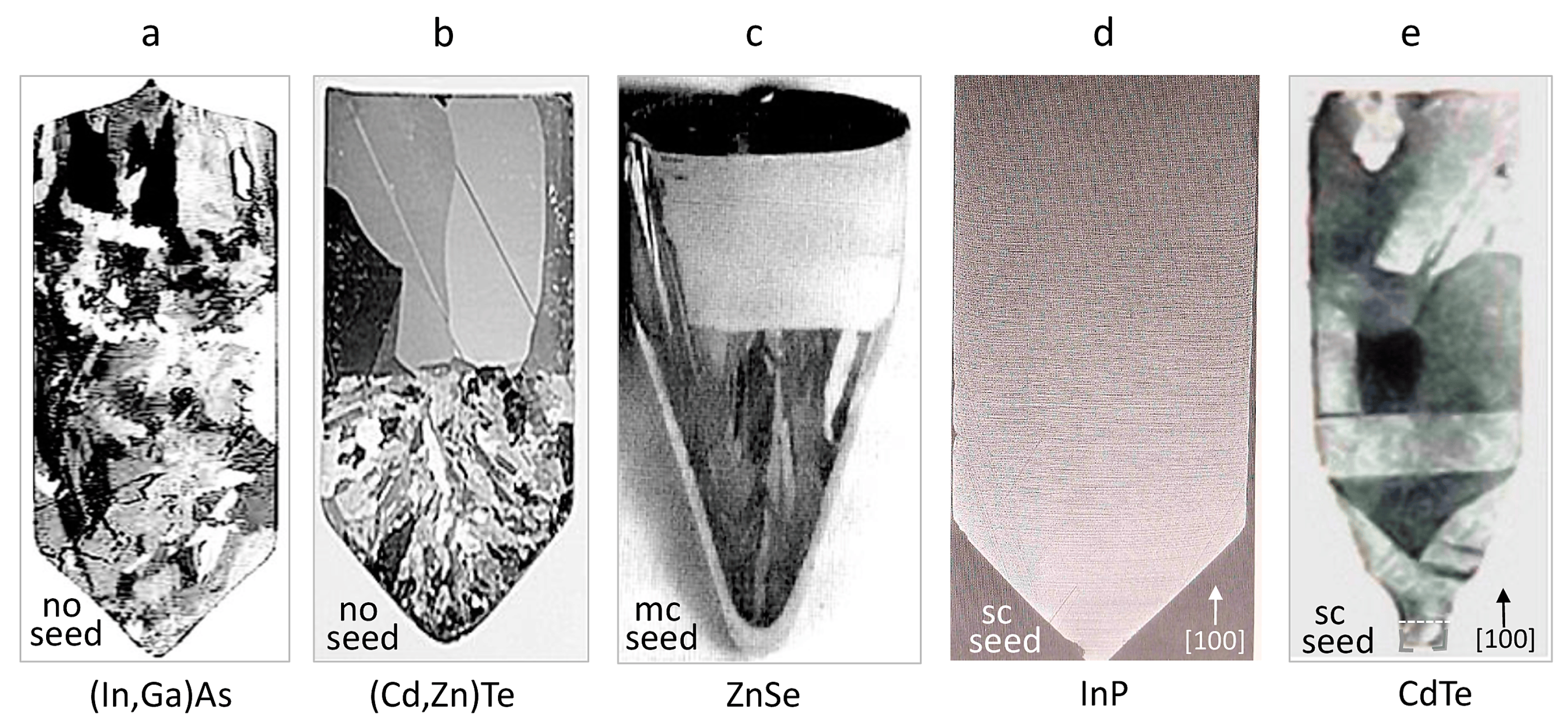
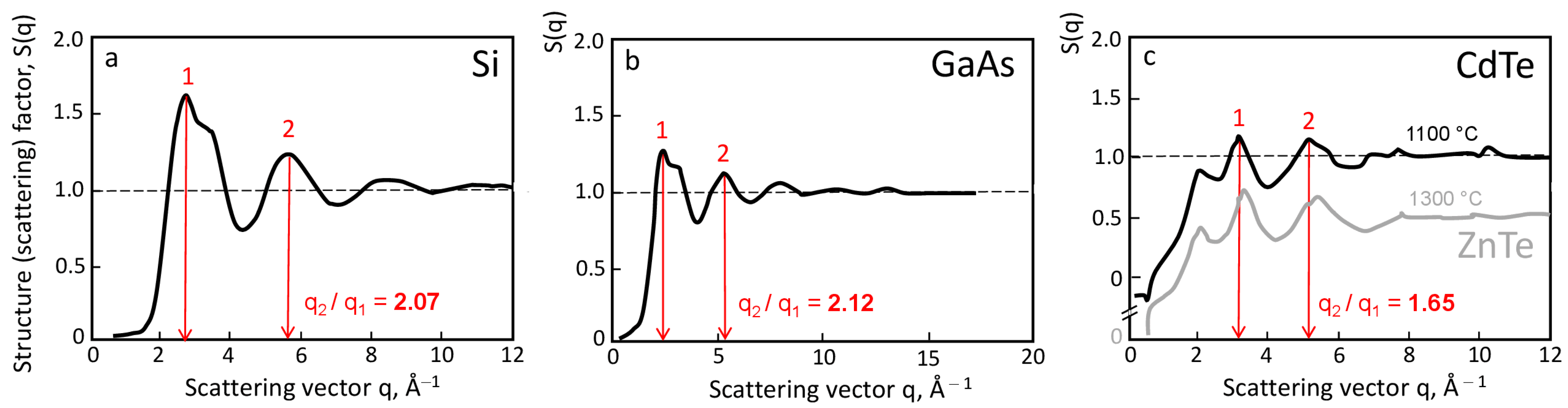
2. Experimental Facts

Figure 1 demonstrates typical features of III–V and II–VI crystals produced without and with a single crystalline seed. Seed-less crystallization of III–V melts always leads to a polycrystalline structure (a) [1] as we know it from the seed-less solidification of silicon ingots for photovoltaics too [2]. On the other hand, crystallization with a seed of any orientation always ensures the correspondingly oriented single-crystal growth (d) [3,4], being the absolute prerequisite for crystal production of high quality and yield. On the contrary, the situation proves to be quite different for II–VI materials. At first, during seed-less crystallization, many spontaneous nuclei are formed in the container tip, but then, as the melting point isotherm is reached, a single crystalline growth abruptly continues on the polycrystalline basis, occasionally consisting of only a few large-angle grains (b) (e.g., [5,6,7,8]). Various authors unanimously observed growth of CdTe, ZnSe, and ZnTe at the unseeded VB or VGF, which was self-orientated mostly towards the <111>, <110>, and sometimes <121> and <122> directions of the prevailing single crystalline region [6,9,10,11,12,13,14]. Even when an intentionally polycrystalline seed is used, like at VB of ZnSe, the growth onto it proceeds as an almost single crystalline structure (c) [9]. And even more so, when a [100]-oriented seed is used, a sudden re-orientation towards divergent orientations takes place (e) [10,15,16]. A quite reasonable agreement between both seed and crystal orientations at VB and VGF of (Cd,Zn)Te has been reported by using the {111} and {211} seeds [8,17,18,19].
As the author of this paper has already emphasized in numerous earlier papers [6,9,20,21,22], such different behavior has to do primarily with the structuring of the melt, which essentially correlates with the binding character. While III–Vs (IVs) show pronounced covalent bonds with a low percentage of ionicity (GaAs: ~30%, Si: 0), the II–VIs are characterized by a markedly higher ionic ratio (CdTe: ~72%, ZnSe: ~63%) [23]. Although both material groups exhibit a binding structure based on the characteristic sp3 hybridization in the II–VI compounds, the center of gravity of the electron bridge between both atomic types is shifted closer to the anion (Te, Se) [24]. As a result, more heteropolarity in the bond strengths with an enhanced degree of ionicity is caused. This is the reason why the mean lattice bond energy in II–VI crystals is about 20% greater than in silicon and III–V crystals [25]. Such binding specificities prove to also be responsible for the high degree of association within the II–VI melts yielding more than 95% at moderate superheating over the congruent melting point Tm [26]. In comparison, the III–V melts show a very small degree of association, i.e., ~5% only [27]. Hence, in II–VI melts, the tetrahedral coordination and, thus, semiconductor behavior remained at an overheating ΔT+ = T – Tm ≤ 10 – 20 K. This has been experimentally proven by neutron diffraction measurements [28] and confirmed by Monte Carlo (MC) [29] as well as molecular dynamic (MD) simulations [30]. Figure 2 compares the structural factor S and scattering vector q of molten silicon, GaAs, and two II–VI materials obtained by neutron diffraction analysis [28,31,32]. Furthermore, Si and GaAs show a ratio of positions of the two first peaks of scattered intensity q2/q1 = 2.07 and 2.12, respectively, which are typical for a sixfold (near liquid metallic) coordinated structure. Moreover, in CdTe and ZnTe liquids the corresponding q2/q1 ratios are 1.72 and 1.70. This indicates that there is a fourfold coordination Z ≈ 4 due to the remained tetrahedral environment compared to the close-packed liquid silicon, III–Vs, and most metals showing coordination numbers near Z ≈ 6.
As has been experimentally proven, a melt association is influenced by the degree and duration of overheating. First, moderate overheating ΔT+ ≤ 10 K of CdTe independently with no undercooling ΔT = TmT = 0 was observed [20,33]. Obviously, the reason is the presence of short-range order associates, which eliminate the energy barrier for nucleation of the solid phase directly at Tm (the differential thermal analysis (DTA) in ref. [33] even indicated “pre-historical” fragments of the solid phase during low overheating). In such cases, the tip of a VB or VGF growth container without an artificial seed consists of only one or very few nuclei that grow into large grains [6,20]. It should be noted that this process is quite impractical because of the permanent uncontrollability of the incorporation kinetics of such associated fragments within a low overheated melt. In fact, in such cases the following crystal structure consists almost entirely of enhanced grains [6]. In contrast, during overheating (markedly over 10 K), a significant structural change of liquid takes place, and the coordination number increases to 6.5 [29]. Obviously, there is a destruction of associates and, at common cooling rates of such melt state, a recovery of conglomerates is depressed by an overly high reactivation energy (this still needs to be proven by proper atomic simulations). As a result, the melt solidifies spontaneously at undercooling values around ΔT ≈ 30 – 40 K [20,33]. Then, after the multinucleated region reached the equilibrium isotherm Tm, the remaining melt volume continues to crystallize to an almost monocrystalline structure if the growth conditions are appropriate. Currently, such procedure is used for CdTe and (Cd,Zn)Te crystal production [8,34,35]. Why this is likely to succeed will be discussed in the next section.
Destruction of the melt association is also possible by dissolution within the excess of anion components as solvents. As it was demonstrated experimentally in marked non-stoichiometric Te- or Se-enriched melt-solutions, the supercooling in seedless CdTe and ZnSe liquids increases markedly compared to that of the stoichiometric melt composition [22,36]. Obviously, a tetrahedrally coordinated melt is closely connected to exact stoichiometry. Otherwise, during Te or Se excess the associated structures become dissolved into molecular or even single atomic configurations. This was confirmed by an ab initio molecular-dynamic simulation [37] (apart from the certain probability of Te cluster [37] and CdTe2 complex generation [29]). Such diluted quasi-unstructured melt benefits the melt solution growth of II–VIs by the traveling heater method (THM), which shows no difficulties with controlled seeding of each orientation. Hence, THM always proceeds successfully by using a single crystalline seed mostly of the same diameter as the growing crystal [38,39,40,41,42].

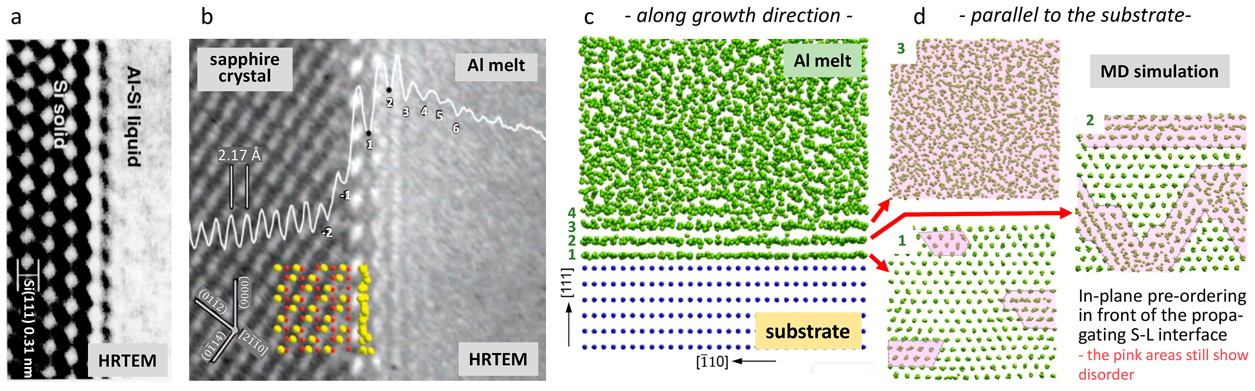
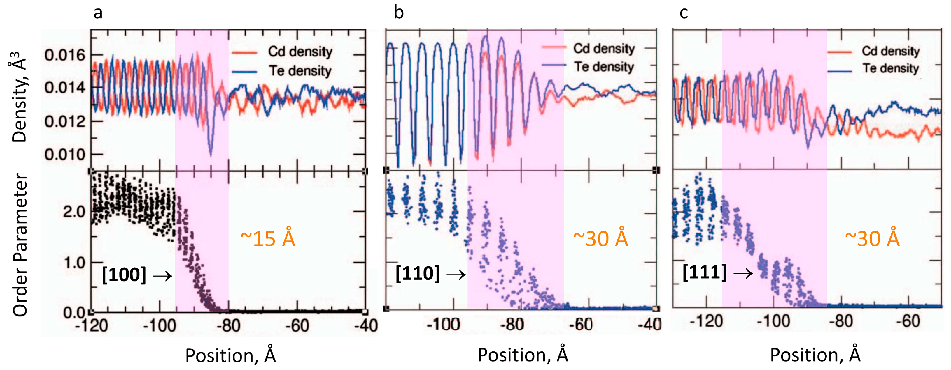
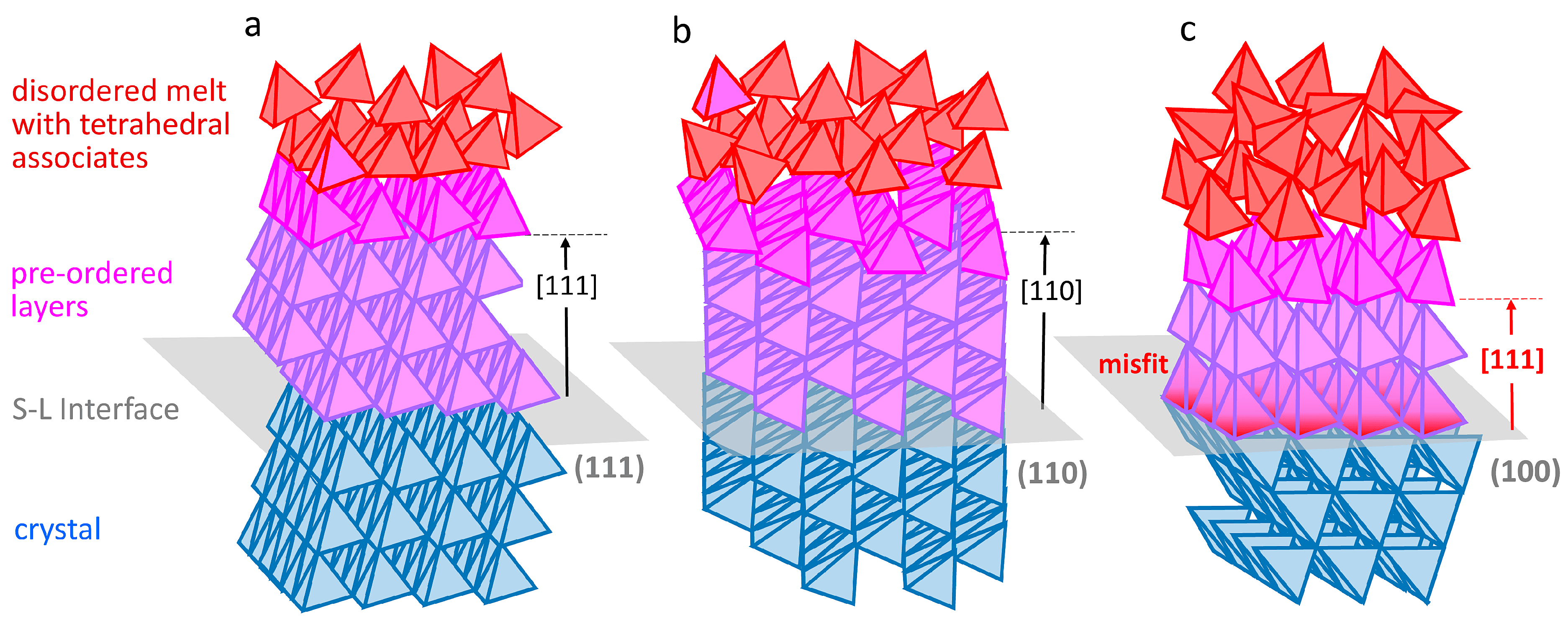
3. Consideration of Melt Pre-Ordering in Front of the Solid–Liquid Interface

The above-mentioned special crystallization behavior of the II–VI crystals must be discussed while taking into account both the self-orientation in the melt caused by high bond ratio of ionicity and the phenomenon of pre-ordering that occurs immediately in front of a propagating solid-liquid (S-L) interface. Generally, during the past few decades, the observation of pre-ordered regions in the melt of diverse materials and alloys has raised great interest in better understanding the interaction between structuring of the liquids and crystallization kinetics [43,44]. In the classical treatment there is the absence of long-range order in liquids as the basic structural difference between liquids and solids. However, it has been ascertained by the continuously improving analytical and simulation techniques that liquid atoms can arrange into a few atomic layers ahead of the S-L interface, resulting in a formation of a structural interstate between the solid and liquid. Such a pre-ordered liquid state is not just a short-lived fluctuation of the liquid, but it proves to be quite a stable intermediate mesophase between the liquid and solid phases.
Meanwhile, there has been an increasing number of high-temperature, high-resolu-tion transmission electron microscopy (HRTEM) images of S-L interfaces, such as molten Al-Si at silicon [45], Al at sapphire [46], or X-ray scattering analyses on crystallizing Au-Si eutectics [47] and ZrCuAl alloys combined with MD simulations [48]. These images deepened our view into the liquid atom arrangements near a solid substrate compared to a seed crystal surface. There are two spatial features of pre-ordering within the liquid to be considered [49]: (i) the formation of layers in the form of liquid density waves transverse to the growth direction with interlayer spacing approaching the crystal’s periodicity, which was already predicted by Mikheev and Chernov [50], and (ii) the in-plane atomic ordering parallel to the solid substrate or seed surface. This detailed study of both effects considered the crystallographic misfit of a given substrate, which revealed the remarkable fact that the atomic layering (i) does not have to necessarily fit the solid lattice, while the transversal in-plane atomic ordering (ii) is strongly dependent on the lattice misfit, meaning it increases with decreasing misfit. Hence, the physical origin of atomic layering within the melt is largely a geometrical effect comparable with granular material against a hard wall [49]. Figure 3 presents two HRTEM images taken from S-L interfaces of Al-Si melt at the Si crystal [45] (a) and liquid Al at the solid Al2O3 [43] (b). Figure 3a shows a relatively small thickness of the still molten transition layer reflecting the crystal structure of the (111)-oriented Si substrate. Moreover, as seen in Figure 3b, several periodic contrast waves indicate a corresponding multi-layer pre-ordering over about six atomic rows. Figure 3c,d show the results of MD modeling of liquid fcc Al on an fcc substrate with a -2% misfit [49]. Again, the Al atoms in the liquid adjacent to the interface exhibit a periodic structure within a few atomic layers according to the above viewpoint (i) (c). Figure 3d represents the in-plane ordering obtained by MD modeling of the time-averaged atomic positions in the first, second, and third interfacial layers according to the above viewpoint (ii). As can be seen, whereas the first and second layers exhibit a still mixed structure of ordered and disordered regions (separated by colored regions), the third layer has a largely disordered structure. This means that in the immediate first layer the influence of the substrate structure is already most evident.
Unfortunately, the author does not yet know any similar high-resolution measurements on the S-L interface of semiconductor compounds, which has to do with their relatively high fugacity. Nevertheless, we can obtain some hints for the III–V and II–VI compounds from Figure 3. First, pre-ordering must be expected in all compounds. However, this effect is less pronounced in III–Vs than in II–VIs due to their missing melt association. Thus, the image (a) showing small transition region should apply to III–Vs too. In comparison, the pre-ordering region in the II–VIs must be broader, like in (b), due to the pronounced effect of melt associations. The pre-ordering is now superimposed by a strong effect of self-orientation caused by tetrahedrally coordinated atomic associates. Therefore, ahead of the S-L interface, i.e., near Tm, a transversal in-plane alignment of these species within the pre-ordered layers takes place, whereby the mutual connection at the imaginary tetrahedral edges is energetically favored. This way, an {111}-oriented layering is already pre-programmed in the melt. Thus, favored growth kinetics will occur if the solid surface orientation approximates such a melt configuration. Otherwise, the pre-orientation of the melt will determine the continuing growth orientation. Of course, with an increasing distance from the interface and temperature, the thermal oscillation and, thus, the deflection from the in-plane arrangement increases, comparable with sequences 1–3 in Figure 3d.
Thus far, to the author’s knowledge, there are only two publications about MD simulation of the atomistic situation at the S-L interface of CdTe by Henager and Morris [51] and partly by Sundaram et al. [11] (Zhou et al. [52] also presented similar modellings but with a focus on the defect formation within the crystal). Figure 4 shows the MD-simulated courses of density and order parameters (being large in the solid phase and small in the liquid phase) along the S-L transition at the {100}, {110}, and {111} interfaces of CdTe [51]. In agreement with the neutron diffraction measurements [28] and melt volume structure simulations [29,30,51], it was confirmed that the CdTe melt retains tetrahedral coordination for temperatures above Tm. Although electrostatic effects, which are due to ionic charges at polar interfaces, were not yet included in this model. The width of the transition region characterized by the decreasing order parameter in front of the {100} interface is of about five atomic rows only. In comparison, at the {110} and {111} interfaces this transition region is about two times larger.
At a first glance, the plots in Figure 4 contradict the simulation results by Freitas and Reed, which were derived from silicon [44], whereupon the interaction between the crystal surface and liquid is mediated by the amount of dangling bonds on the crystal surface. They concluded that the strong liquid pre-ordering should be observed at atomically rough interfaces, such as (100), due to their stronger interface interaction with the liquid, as they present more dangling bonds when compared to atomically smooth interfaces, such as (111), and related vicinals. This is certainly correct for silicon and III–Vs showing dissociated melts of an atomic sixfold package without any tetrahedral coordination (see Figure 2a,b). However, at a fourfold coordination with tetrahedral self-structuring, like in the II–VI liquids (see Figure 2c), the growth kinetics are no longer determined solely by the number of dangling bonds to be saturated by adsorption of molecules or single atoms, but predominantly by the adaptability of the tetrahedrally patterned melt layers. Thus, in agreement with Figure 5, the {111} and partially the {110} solid surface orientations are best able to adopt pre-layered and {111} pre-oriented tetrahedrally aligned melt configurations. Therefore, the width of the order parameter is extented further into the melt (Figure 4b,c). Certainly, such melt structuring always retains its statistical character of being temporally built-up and broken down even with increasing temperature. Then, it is possible that such oscillating behaviors of the pre-oriented layers can often cause {112} and {122} re-orientations, resulting in a vicinal surface configuration with favorable step-by-step growth kinetics.
It is important to note that in the II–VI melts one has to distinguish between the statistical average of tetrahedral coordination proven by neutron diffraction analysis [29,30,51] and the presence of rudimentary fractions at low superheating as was pointed out by Shcherbak [33]. The rudimentary fractions are irrecoverably destroyed by high superheating [20,29,33], while the tetrahedral melt coordination is driven back by the decreasing melt temperature Tm.
In Figure 5 the tetrahedral imaginations of {111}-, {110}-, and {100}-oriented crystal interfaces of CdTe in contact with the probable pre-ordered and pre-oriented melt are sketched. A layered arrangement of in-plane aligned tetrahedrons is presented in the melt ahead of the S-L interface, i.e., near Tm. Obviously, both the effect of pre-ordering and the self-orientation are in accordance and, thus, such liquid configuration best fits the {111} interface (a) and, with tilting, fits the {110} interface too (b). The often experimentally observed slight re-orientations of the grown CdTe and (Cd,Zn)Te crystals along <112> and <122> directions (see Section 2), with small inclination angles to the <111> direction of 19°47′ and 15°79′, respectively, favors the step-by-step growth instead of impeding it at an atomically smooth (singular) {111} plane. In contrast, at the {100} interface the situation is more complex. Following the experimental results that indicate that an artificial [100] seeding almost failed, the quasi {111} pre-orientation of the pre-ordered melt layers showed the continuing growth direction. Of course, this results in a lattice compression at the interface with a probable generation of misfit dislocations (it is well known from heteroepitaxy of the (111)-oriented CdTe on (100) foreign substrates). Hence, the growth orientation is also determined by melt pre-orientation on a polycrystalline basis, as shown in Figure 1b,c.
A further well-known effect of orientation change must also be taken into account. Due to the extremely low stacking fault energy, even at stoichiometric Tm of CdTe (10 × 10−7 J cm−2 compared to 55 × 10−7 J cm−2 in GaAs), the twinning probability is very high. As a result, the <100> orientation is abruptly changed into the <122> direction via a congruent twin plane of first order [53]. Of course, that also happens in III–Vs but with a lower probability due to the higher stacking fault energy (the exception is InP with a comparable value to that of CdTe).
One of the recommendations of the present author supports the partial previously mentioned hypotheses, which states that the transfer into exact evidences with the help of proper atomistic simulation is achieved by considering the long-range force fields of the high bond ionicity ratio of the II–VI melts.

4. Selected Consequences for Crystal Growth Methodology

As it was mentioned in Section 2, due to the lack of strong associations within the non-stoichiometric melt solutions, the growth of CdTe and (Cd,Zn)Te crystals from a Te-rich zone by THM seems to be favored. In fact, the THM at reduced growth temperature around 800 °C is widely practiced [38,39,40,41,42]. Successful artificial seeding of each quasi-orientation (mostly in <111> direction), the elimination of twinning due to the increased stacking fault energy, and the reduction in dislocation density (e.g., the mean EPD of undoped THM Cd0.96Zn0.04Te crystals amounts to ~104 cm−2) are the decisive advantages. Currently, the monocrystalline yield of as-grown THM ingots shows >80% compared to VB/VGF at the stoichiometric melt with a much lower yield of <50%. However, the maximum achievable THM crystal diameter of 3 inches (4 inch in test) is only adequate for devices of relatively small dimensions, such as photo counting detectors for computer tomography. Moreover, much larger diameters of 5–6 inches are necessary to produce large-area (Cd,Zn)Te substrates for epitaxial (Hg, Cd)Te thin films used in IR photoconductor devices (for example, [54]). Consequently, such case improvements must be found in the crystallization from melts.
As it was demonstrated in Section 1 and Section 2, conventional VB and VGF growth of 6–8 inch crystals from the stoichiometric melt succeeds with the III–Vs, but has so far proven to be less suitable for II–VI growth of same diameters. Especially the recommended high superheating of the II–VI melt volume before the crystallization induces a marked melting back or even complete melting of an artificial seed. Therefore, large-area {111}- and {122}-oriented CdTe and (Cd,Zn)Te wafers are mostly cut out from the largest grain of un-seeded former high-overheated VB/VGF ingots and result in enhanced costs. Hence, more efforts should be made to find a clever combination between melt superheating and artificial <111> and <112> seedings. For instance, a quite good result of 80% single crystallinity was obtained by Xu et al. [18] using 40 mm long seed crystals of such orientation in order to remelt it partially. Saucedo et al. [55] applied a modified Bridgman setup, which enabled high melt superheating before the subsequently cooled melt that contacted the seed crystal by a swiveling furnace. Also, the liquid-encapsulated Czochralski growth (LEC) with inherent melt overheating before the seed is dipped was used by Hobgood et al. [56]. However, it failed for CdTe by multi-twinning due to the extraordinarily high and inhomogeneous axial and radial temperature gradients and oscillations. Actually, affected by this result, no more improved LEC was reported in the following period up until today. A low-temperature gradient vapor pressure-controlled Czochralski method (VCz) is much more promising [57], as it is used successfully for high-quality 6-inch GaAs but not yet for CdTe and (Cd,Zn)Te. Such a project would have the additional advantage of an in situ stoichiometry control by an extra integrated Cd source.
Finally, a modified method of contactless directional crystallization of 4 inches and larger CdTe crystals, introduced by Ivanov [58], attracts the attention. The crystallization starts by self-seeding on the free surface of the previously superheated melt and proceeds by slowly cooling along a small inverse temperature gradient, in a top-to-bottom pattern. Compared with the Kyropoulos method (successfully applied in the ZnTe single-crystal growth [59]), there is no contact with the container wall during the whole growth process, which results in markedly reduced danger of the grain and twinning generation. Obviously, there is a favorable condition of contactless nucleation by {111} self-orientation in the center of a free melt surface promoted by the tetrahedral in-plane alignment. Furthermore, the enhanced buoyancy convection proves to be helpful in keeping residual conglomerates away from the growing S-L interface. The recent numeric simulation of such a whole-growth process of 4-inch (Cd,Zn)Te crystals showed that there are favorable convective conditions for a slightly convex-to-flat interface and axial composition homogeneity [60]. Consequently, single crystals with a yield of 80–100% are obtained. For instance, Franc et al. [61] reported the growth of 4-inch (Cd,Zn)Te crystals by the same method showing 80% single crystallinity. They controlled the stoichiometry in situ by an additional Cd source over the melt volume. Recently this in site growth principle after annealing was claimed by JX Nippon Mining & Metals Co. [62].

5. Conclusions

The nucleation behavior, self-orientation and subsequent growth at crystallization of II–VI compounds from the melt, differing markedly from III–Vs, was discussed. Some experimentally proven and modeled explanations were given. It is safe to assume that decisional influence proves to be the characteristic high percentage of bond ionicity of II–VIs. Both neutron diffraction measurements and molecular dynamic simulations revealed that CdTe melts, when moderately superheated over the congruent melting point Tm, keep its tetrahedral coordination consistent with the crystalline phase. Also, superheating–supercooling experiments indicate the still presence of associates, even pre-historical conglomerates of up to at least 10 K over Tm.
After higher superheating of the melt at seedless VB or VGF growth, a multi-nucleated polycrystalline region is formed within the container tip. The remaining melt volume continues to crystallize in an monocrystalline fashion, often consisting of a few large grains with predominantly <110> and <111>, and sometimes <112> and <122> orientations, but almost never in a <100> direction. Even the artificial <100> seeding fails by a sudden reorientation. Obviously, the following two effects are superimposed: (i) pre-ordering forced by the solid surface that generates transverse density layering in front of the S-L interface, and (ii) {111} self-orientation via tetrahedral in-plane alignment along the pre-ordered layers. A fitting growth kinetics seems to only be possible when such a melt configuration conforms to the crystal structure, like the {111} but hardly the {100}. Otherwise, the liquid self-orientation determines the continuing crystal orientation. Due to the extremely low stacking fault energy, the twinning probability is also enhanced and creates an abrupt change of the <100> orientation into the <122> direction by a congruent twin plane.
It is the emphatic recommendation of the author such partly hypothetic considera-tion to transfer into exact evidences with the help of more proper atomistic simulation by considering the high ratio of bond ionicity.
In conclusion, better understanding of the II–VI melt configuration and its controllability will help improve the growth methodology of 4–6-inch crystals from the stoichiometric melt. It seems that the fine-tuning of contactless self-seeding on the free surface of the previously superheated melt and the subsequent crystallization in an inverse low-temperature gradient, accompanied by in situ stoichiometry control and in situ annealing, seems to be quite a suitable growth concept.

Funding

This research received no external funding.

Data Availability Statement

The original contributions presented in the study are included in the article, further inquiries can be directed to the author.

Conflicts of Interest

The author declares no conflicts of interest.

References

  1. Hashio, K.; Tatsumi, M.; Kato, H.; Kinoshita, K. Directional Solidification of InxGa1−xAs. J. Cryst. Growth 2000, 10, 471–477. [Google Scholar] [CrossRef]
  2. Kiessling, F.-M.; Büllesfeld, F.; Dropka, N.; Frank-Rotsch, C.; Müller, M.; Rudolph, P. Characterization of mc-Si directionally solidified in travelling magnetic fields. J. Cryst. Growth 2012, 360, 81–86. [Google Scholar] [CrossRef]
  3. Monberg, E. Bridgman and Related Growth Techniques. In Handbook of Crystal Growth, Growth Techniques; Hurle, D.T.J., Ed.; Elsevier Science B.V.: Amsterdam, The Netherlands, 1994; Volume 2A, pp. 99–212. [Google Scholar]
  4. Rudolph, P.; Matsumoto, F.; Fukuda, T. Studies on interface curvature during vertical Bridgman growth of InP in a flat-bottom container. J. Cryst. Growth 1996, 158, 43–48. [Google Scholar] [CrossRef]
  5. Casagrande, L.G.; Di Marzio, D.; Lee, M.B.; Larson, D.J.; Dudley, M.; Fanning, T. Vertical Bridgman growth and characterization of large-diameter single-crystal CdTe. J. Cryst. Growth 1993, 128, 576–581. [Google Scholar] [CrossRef]
  6. Rudolph, P. Fundamental studies on Bridgman growth of CdTe. Progr. Cryst. Grow. Charact. Mat. 1994, 29, 275–381. [Google Scholar] [CrossRef]
  7. Choi, B.W.; Wadley, H.N.G. In situ studies of Cd1−xZnxTe nucleation and crystal growth. J. Cryst. Growth 2000, 208, 219–230. [Google Scholar] [CrossRef]
  8. Kakkireni, S.; Murugesan, M.; Montag, B.; McCloy, J. Seeded Crystal Growth of Cd-Zn-Te (CZT) Assisted via Numerical Modelling. In Emerging Materials; Thoutam, L.R., Tayal, S., Ajayan, J., Eds.; Springer Nature Singapore Pte Ltd.: Singapore, 2022; pp. 103–133. [Google Scholar] [CrossRef]
  9. Rudolph, P.; Schäfer, N.; Fukuda, T. Crystal Growth of ZnSe from the melt. Mater. Sci. Eng. Rep. 1995, 15, 85–133. [Google Scholar] [CrossRef]
  10. Feigelson, R.S.; Route, R.K. Improved Techniques for the Growth of High Quality Cadmium Telluride Crystals; Final Rep. CMR-85-3. Center for Mat. Res.; Stanford University: Stanford, CA, USA, 1985; pp. 1–52. [Google Scholar]
  11. Sundaram, S.K.; Henager, S.K., Jr.; Edwards, D.J.; Schemer-Kohrn, A.L.; Bliss, M.; Riley, B.R. Electron backscatter diffraction analysis of a CZT growth tip from a vertical gradient freeze furnace. J. Cryst. Growth 2011, 329, 12–19. [Google Scholar] [CrossRef]
  12. Kulakov, M.P.; Kulakovskii, V.D.; Fadeev, A.V. Twinning in ZnSe crystals obtained from melt under pressure. Izv. Akad. Nauk. SSSR Neorgan. Mater. 1976, 12, 1867–1869. [Google Scholar]
  13. Kikuma, I.; Furukoshi, M. Direct Observation of the 3c-2h Transformation in ZnSe by High-Temperature X-Ray Diffraction. J. Cryst. Growth 1985, 71, 136–140. [Google Scholar] [CrossRef]
  14. Asahi, T.; Arakawa, A.; Sato, K. Growth of large-diameter ZnTe single crystals by the vertical gradient freezing method. J. Cryst. Growth 2001, 229, 74–78. [Google Scholar] [CrossRef]
  15. Balbaşı, Ö.B.; Ünal, M.; Genç, A.M.; Çelik, G.; Parlak, M.; Turan, R. Investigation of seeded vertical gradient freeze (VGF) growth of CdZnTe bulk crystals. J. Cryst. Growth 2022, 584, 126573. [Google Scholar] [CrossRef]
  16. Sato, K.; Seki, Y.; Matsuda, Y.; Oda, O. Recent developments in II–VI substrates. J. Cryst. Growth 1999, 197, 413–422. [Google Scholar] [CrossRef]
  17. Wang, T.; Jie, W.; Xu, Y.; Zha, G. Characterization of CdZnTe crystal grown by bottom-seeded Bridgman and Bridgman accelerated crucible rotation techniques. Trans. Nonferrous Met. Soc. China 2009, 19, s622–s625. [Google Scholar] [CrossRef]
  18. Xu, Y.; Jie, W.; Sellin, P.J.; Wang, T.; Fu, L.; Zha, G.; Veeramani, P. Characterization of CdZnTe Crystals Grown Using a Seeded Modified Vertical Bridgman Method. IEEE Trans. Nucl. Sci. 2009, 56, 2808–2813. [Google Scholar] [CrossRef]
  19. Chao, X.; Juan, Z.; Changhe, Z.; Shangshu, L.; Ruiyun, S. Advancements in Iso-Diameter seeded growth of CdZnTe crystals: A numerical modeling approach and applications in liquid phase Epitaxy. J. Cryst. Growth 2024, 633, 127670. [Google Scholar] [CrossRef]
  20. Mühlberg, M.; Rudolph, P.; Laasch, M.; Treser, E. The correlation between superheating and supercooling in CdTe melts during unseeded Bridgman growth. J. Cryst. Growth 1993, 128, 571–577. [Google Scholar] [CrossRef]
  21. Rudolph, P.; Umetsu, K.; Koh, H.J.; Fukuda, T. Correlation between ZnSe Crystal Growth Conditions from Melt and Generation of Large-Angle Grain Boundaries and Twins. Jpn. J. Appl. Phys. 1994, 33, 1991–1994. [Google Scholar] [CrossRef]
  22. Rudolph, P.; Koh, H.J.; Schäfer, N.; Fukuda, T. The crystal perfection depends on the superheating of the mother phase too—Experimental facts and speculations on the “melt structure” of semiconductor compounds. J. Cryst. Growth 1996, 166, 578–582. [Google Scholar] [CrossRef]
  23. Adachi, S. Properties of Group-IV, III–V and II–VI Semiconductors; John Wiley & Sons, Ltd.: Chichester, UK, 2005. [Google Scholar] [CrossRef]
  24. Merad, A.E.; Kanoun, M.B.; Merad, G.; Cibert, J.; Aourag, H. Full-potential investigation of the electronic and optical properties of stressed CdTe and ZnTe. Mater. Chem. Phys. 2005, 92, 333–339. [Google Scholar] [CrossRef]
  25. Pattanaik, A.; Tripathy, S.K.; Naik, P.; Meher, D.K. Structural and elastic properties of binary semiconductors from energy gaps. Appl. Phys. 2021, 127, 14. [Google Scholar] [CrossRef]
  26. Jordan, A.S. A Theory of Regular Associated Solution Applied to the Liquidus Curves of the Zn-Te and Cd-Te System. Metall. Trans. 1970, 1, 239–249. [Google Scholar] [CrossRef]
  27. Weiser, K. Pressure-Temperature-Composition (P-T-x) Diagrams. In Compound Semiconductors, Preparation of III–V Compounds; Willardson, R.K., Goering, K.H.L., Eds.; Reinhold: New York, NY, USA, 1962; Volume 1, pp. 472–481. [Google Scholar]
  28. Gaspard, J.P.; Raty, J.Y.; Céolin, R.; Bellissent, R. Local orders in II–VI liquid compounds. J. Non-Cryst. Solids 1996, 205–207, 75–78. [Google Scholar] [CrossRef]
  29. Godlevsky, V.V.; Jain, M.; Derby, J.J.; Chelikowsky, J.R. First principles calculations of liquid CdTe at temperatures above and below the melting point. Phys. Rev. 1999, 60, 8640–8649. [Google Scholar] [CrossRef]
  30. Dalgic, S.; Colakogullari, M. The structural properties of the liquid CdTe based on Reverse Monte Carlo modelling. J. Cryst. Growth 2007, 353, 1936–1940. [Google Scholar] [CrossRef]
  31. Gaspard, J.P. Structure of Melt and Liquid Alloys. In Handbook of Crystal Growth, 2nd ed.; Fundamentals: Thermodynamics and Kinetics; Nishinaga, T., Ed.; Elsevier: Amsterdam, The Netherlands, 2015; Volume IA, pp. 401–443. [Google Scholar] [CrossRef]
  32. Bergman, C.; Bichara, C.; Chieux, P.; Gaspard, J.P. On The Atomic Structure Of Liquid GaAs. J. Phys. Colloq. 1985, 46, C8-97. [Google Scholar] [CrossRef]
  33. Shcherbak, L. Pre-transition phenomena in CdTe near the melting point. J. Cryst. Growth 1999, 197, 397–405. [Google Scholar] [CrossRef]
  34. Crocco, J.; Bensalah, H.; Zheng, H.; Carcelén, V.; Diéguez, E. Influence of SiC pedestal in the growth of 50 mm CZT by Vertical gradient freeze method. J. Cryst. Growth 2012, 360, 92–94. [Google Scholar] [CrossRef]
  35. Zappettini, A. Cadmium Telluride and Cadmium Zinc Telluride. In Single Crystals of Electronic Materials—Growth and Properties; Fornari, R., Ed.; Woodhead Publishing, imprint Elsevier: Duxford, UK, 2019; pp. 273–301. [Google Scholar] [CrossRef]
  36. Kikuma, I.; Sekine, M.; Furukoshi, M. Growth of ZnSe Crystals Free From Rod-Like Low Angle Grain Boundaries from the Melt Under Argon Pressure. J. Cryst. Growth 1986, 75, 609–612. [Google Scholar] [CrossRef]
  37. Moskvin, P.; Khodakovskya, V.; Rashkovetskyi, L.; Stronski, A. Polyassociative model of A2B6 semiconductor melt and p-T-x equilibria in Cd–Hg–Te system. J. Cryst. Growth 2008, 210, 2617–2626. [Google Scholar] [CrossRef]
  38. Shiraki, H.; Funaki, M.; Ando, Y.; Tachibana, A.; Kominami, S.; Ohno, R. THM growth and characterization of 100 mm diameter CdTe single crystals. IEEE Trans. Nucl. Sci. 2009, 56, 1717–1723. [Google Scholar] [CrossRef]
  39. Mackenzie, J.; Kumar, F.J.; Chen, H. Advancements in THM-Grown CdZnTe for Use as Substrates for HgCdTe. J. Electron. Mat. 2013, 42, 3129–3132. [Google Scholar] [CrossRef]
  40. Prokesch, M.; Soldner, S.A.; Sundaram, A.G. CdZnTe detectors for gamma spectroscopy and x-ray photon counting at 250 × 106 photons/(mm2 s). J. Appl. Phys. 2018, 24, 044503. [Google Scholar] [CrossRef]
  41. Zhou, B.; Jie, W.; Wang, T.; Yin, L.; Yang, F.; Zhang, B.; Xi, S.; Dong, J. Modification of growth interface of CdZnTe crystals in THM process by ACRT. J. Cryst. Growth 2018, 483, 281–284. [Google Scholar] [CrossRef]
  42. Vijayakumar, P.; Amaladass, E.P.; Ganesan, K.; Sarguna, R.M.; Roy, V.; Ganesamoorthy, S. Development of travelling heater method for growth of detector grade CdZnTe single crystals. Mat. Sci. Semicond. Proc. 2024, 169, 107897. [Google Scholar] [CrossRef]
  43. Kaplan, W.D.; Kauffmann, Y. Structural Order in Liquids Induced by Interfaces with Crystals. Annu. Rev. Mater. Res. 2006, 36, 1–48. [Google Scholar] [CrossRef]
  44. Freitas, R.; Reed, E.J. Uncovering the effects of interface-induced ordering of liquid on crystal growth using machine learning. Nat. Commun. 2020, 11, 3260. [Google Scholar] [CrossRef] [PubMed]
  45. Arai, S.; Tsukimoto, S.; Muto, S.; Saka, H. Direct observation of the atomic structure in a solid–liquid interface. Microsc. Microanal. 2000, 6, 358–361. [Google Scholar] [CrossRef] [PubMed]
  46. Gandman, M.; Kauffmann, Y.; Koch, C.T.; Kaplan, W.D. Direct Quantification of Ordering at a Solid-Liquid Interface Using Aberration Corrected Transmission Electron Microscopy. Phys. Rev. Lett. 2013, 110, 086106. [Google Scholar] [CrossRef]
  47. Schülli, T.U.; Daudin, R.; Renaud, G.; Vaysset, A.; Geaymond, O.; Pasture, A. Substrate-enhanced supercooling in AuSi eutectic droplets. Nature 2010, 464, 1174–1177. [Google Scholar] [CrossRef]
  48. Zhao, J.; Tang, Z.; Kelton, K.F.; Liu, C.T.; Liaw, P.K.; Inoue, A.; Shen, X.; Pan, S.; Johnson, M.L.; Chen, G.; et al. Evolution of the atomic structure of a supercooled Zr55Cu35Al10 liquid. Intermetallics 2017, 82, 53–58. [Google Scholar] [CrossRef]
  49. Men, H.; Fan, Z. Prenucleation Induced by Crystalline Substrates. Metall. Mater. Trans. A 2018, 49, 2766–2777. [Google Scholar] [CrossRef]
  50. Mikheev, L.V.; Chernov, A.A. Mobility of a diffuse simple crystal-melt interface. J. Cryst. Growth 1991, 112, 591–596. [Google Scholar] [CrossRef]
  51. Henager, C.H., Jr.; Morris, J.R. Atomistic simulation of CdTe solid-liquid coexistence equilibria. Phys. Rev. 2009, 80, 245309. [Google Scholar] [CrossRef]
  52. Zhou, X.W.; Ward, D.K.; Wong, X.W.; Doty, F.P. Melt-Growth Dynamics in CdTe Crystals. Phys. Rev. Lett. 2012, 108, 245503. [Google Scholar] [CrossRef]
  53. Durose, K.; Russell, G. Twinning in CdTe. J. Cryst. Growth 1990, 101, 246–250. [Google Scholar] [CrossRef]
  54. Rogalski, A. HgCdTe Photodetectors. In Mid-Infrared Optoelectronics. Materials, Devices, and Applications; Tournié, E., Laurent, C., Eds.; Elsevier Ltd.: Amsterdam, The Netherlands, 2020; pp. 235–335. [Google Scholar] [CrossRef]
  55. Saucedo, E.; Rudolph, P.; Dieguez, E. Modified Bridgman growth of CdTe crystals. J. Cryst. Growth 2008, 310, 2067–2071. [Google Scholar] [CrossRef]
  56. Hobgood, H.M.; Swanson, B.W.; Thomas, R.N. Czochralski growth of CdTe and CdMnTe from liquid encapsulated melts. J. Cryst. Growth 1987, 85, 510–520. [Google Scholar] [CrossRef]
  57. Neubert, M.; Rudolph, P. Growth of semi-insulating GaAs crystals in low temperature gradients by using the vapour pressure controlled Czochralski method (VCz). Progr. Cryst. Growth Charact. Mat. 2001, 43, 119–185. [Google Scholar] [CrossRef]
  58. Ivanov, Y.I. Preparation of CdTe and CdZnTe Single-Crystalline Ingots 100 mm in Diameter by a Modified Obreimov–Shubnikov Method. Russ. J. Inorg. Chem. 2015, 60, 1816–1823. [Google Scholar] [CrossRef]
  59. Asahi, T.; Yabe, T.; Sato, K.; Arakawa, A. Growth of large diameter ZnTe single crystals by the LEK method. J. Alloys Compd. 2004, 33, 651–653. [Google Scholar] [CrossRef]
  60. Pavlyuk, M.D.; Sukhanov, E.A.; Zykov, M.P.; Volchkov, I.S.; Kanevskii, V.M.; Subbotin, I.A.; Podurets, K.M.; Pavlyuk, B.F.; Ivanov, Y.M. Mathematical Simulation of the Process of Growing a CdTe Single Crystal by the Obreimov–Shubnikov Method. Phys. Solid State 2020, 62, 1–7. [Google Scholar] [CrossRef]
  61. Crocco, J.; Franc, J.; Zazvorka, J.; Hlidek, P.; Dieguez, E.; Babentsov, V.; Sochinskyi, M.V.; James, R.B. Semi-Insulated Cd1−xZnxTe Grown by the Vertical Gradient Freeze Method. IEEE Trans. Nucl. Sci. 2012, 59, 1516–1521. [Google Scholar] [CrossRef]
  62. Itani, K.; Murakami, K.; Yamada, K. Compound Semiconductor and Method for Producing the Same. U.S. Patent US11552174B2, 1 October 2023. [Google Scholar]
Figure 1. Longitudinal cut of unseeded and seeded III–V and II–VI crystals: (a) In0.3Ga0.7As polycrystal directionally solidified without seed [1]; (b) Cd0.96Zn0.04Te VGF crystal spontaneously multi-nucleated without the seed, but continued its monocrystalline growth with a few large grains (courtesy of Y. Ergunt from Aselsan Inc., Ankara, Türkiye); (c) ZnSe VGF crystal grown on a multicrystalline (mc) seed [9] (a thin layer of condensate formed around the seed); (d) transmission X-ray topography of an InP slice taken from a VGF crystal grown on a single-crystalline (sc) [100]-oriented seed [3]; (e) X-ray synchrotron topography of a CdTe slice taken from a VB boule crystallized on a [100]-oriented seed (courtesy of R.S. Feigelson, Stanford, CA, USA); (a,c,d) with permission from Elsevier.
Crystals 14 01067 g001
Figure 2. Structure factors of liquid silicon [31] (a), GaAs [32] (b), and II–VI compounds CdTe and ZnTe [28] (c) just above the congruent melting point Tm obtained by neutron-scattering analysis. The ratio of two first peaks of the scattered intensity q2/q1 indicate the coordination number Z in a molten state (~2 and ~1.7 stand for Z = 6 and 4, respectively); adapted with permission from Elsevier (a,c) and IOP Publishing Ltd. (b).
Crystals 14 01067 g002
Figure 3. Images demonstrating the principle of pre-ordering in front of propagating S-L interfaces: (a) HRTEM of a solid Si–liquid Al–Si alloy, viewed along the Si-[110]-direction. A pre-ordered atomic row in front of the solid Si (111) plane is visible [45]; (b) HRTEM snapshot showing pre-ordered molten aluminum at the interface with a sapphire crystal. The atom positions in Al2O3 (red for O and yellow for Al) were determined by contrast matching between simulated and experimental images. Six rows in front of the IF show liquid density waves with interlayer spacing approaching the crystal’s periodicity [43]; (c,d) MD-simulated aluminum melt structure on a solid fcc substrate with a lattice misfit of −2%. The Al atoms in the liquid adjacent to the interface exhibit a layered structure within of few atomic rows 1–4 (c). The areas parallel to the substrate of the first and second layers already show a mixed structure of ordered and still disordered regions prior to the third layer with a largely disordered liquid structure [49] (d); adapted with permission from Microscopy Soc. of America (a), AAAS (b), and the Minerals, Metals, and Mat. Soc. (c,d).
Crystals 14 01067 g003
Figure 4. MD-simulated fine-scale density and order-parameter plots as functions of position normal to the S-L interface for [100] (a), [110] (b), and [111] (c) directions in CdTe (adapted from ref. [51] with permission from the American Physical Soc.): (a) sharp [100] IF with a few remnants of tetrahedral pre-ordering for ~15 Å into the melt; (b) and (c) [110] and [111] IFs with broader tetrahedrally pe-ordered transition regions of ~30 Å, respectively.
Crystals 14 01067 g004
Figure 5. Sketch of the probable order sequence near the S-L interface of CdTe according to experimental findings drawn in a tetrahedral imagination: (a,b) adaptation of the pre-ordered layers to the (111)- and (110)-oriented interface, respectively; (c) abrupt orientation change due to the disagreement of the in-plane aligned tetrahedral shape in front of the interface of (100) orientation saturating three dangling bonds insteat of only two. This results in a compressive lattice misfit. Because of the lack of orientation inducement of the crystal in (c), the width of the pre-ordered region is much smaller than in other cases (a,b).
Crystals 14 01067 g005
Disclaimer/Publisher’s Note: The statements, opinions and data contained in all publications are solely those of the individual author(s) and contributor(s) and not of MDPI and/or the editor(s). MDPI and/or the editor(s) disclaim responsibility for any injury to people or property resulting from any ideas, methods, instructions or products referred to in the content.

