1. Introduction
Semiconductor self-assembled quantum dot (QD) nanostructures have garnered significant attention due to their potential in a wide range of opto-electronic applications, including light-emitting diodes [
1], lasers [
2], and solar cells [
3]. QDs are of significant interest in research as ideal candidates for high-quality single-photon sources [
4,
5] and crucial for applications like polarization-based two-photon entanglement [
6,
7] and nanolasers [
8]. Key performance metrics for these applications include near-transform-limited emission and near-indistinguishable photons, which are essential for ensuring high-quality quantum optical processes [
4].
Various growth techniques and material systems are employed to fabricate QDs that emit at different wavelengths. For instance, GaAs QDs and InAs QDs are widely studied for their distinct properties. GaAs QDs are typically created by filling nanoholes, which are formed in an AlGaAs matrix via local droplet etching (LDE), with GaAs [
9,
10]. These QDs emit in the 700 nm to 800 nm wavelength range [
11], and they possess highly symmetrical, strain-free structures with low fine structure splitting [
11,
12]. Charge control finally makes these QDs excellent single-photon sources emitting highly indistinguishable photons [
13], even from remote emitters [
14]. However, the telecom O-band and C-band, critical for technological applications due to minimal absorption losses in optical fibers, cannot be achieved with GaAs QDs.
In contrast, the mechanism behind InAs QD growth on GaAs is based on strain relaxation, owing to the 7% lattice mismatch between InAs and GaAs [
15]. This mismatch results in a transition from the Frank–Van der Merwe to the Stranski–Krastanov (SK) growth mode, which occurs after the critical layer thickness of about 1.5 monolayers (ML) of InAs is exceeded [
15]. InAs QDs typically emit at longer wavelengths, with ground-state emissions around 1200 nm. However, in situ growth techniques have been developed to tune the emission wavelength. The indium flush technique [
16] enables blueshifting of the emission down to 900 nm [
17] by partially capping the QDs with GaAs and ramping up the temperature to remove uncovered InAs. Another approach involves capping InAs QDs with an InGaAs strain-reduction layer (SRL), which further redshifts their emission, allowing for operation in the telecom O-band at 1310 nm and beyond [
18].
InAs QDs have been established as high-quality single-photon sources [
5]. However, compared to locally droplet-etched (LDE) QDs, they exhibit some notable disadvantages. Strain within InAs QDs [
19], as well as slight asymmetries in their confinement potential, result in higher fine structure splitting [
20], which can limit their performance in certain applications. Additionally, controlling the density of InAs QDs is more challenging, and their emission wavelength is harder to fine-tune compared to LDE QDs. In contrast, LDE QDs offer more precise emission wavelength control simply by varying the amount of material used to fill the nanoholes [
21], making them a promising candidate for tailored photonic devices.
Research efforts have already explored the development of LDE QDs for the telecom C-band. For example, Cao et al. [
22] investigated LDE growth on an InAlAs matrix grown on InP substrates, and Deutsch et al. [
23] demonstrated QDs created by filling nanoholes with InGaAs. However, the suitability of these QDs as high-quality single-photon sources has not yet been confirmed. In this work, a different approach is introduced, combining both LDE and SK growth methods. Specifically, nanoholes are etched into a GaAs matrix, followed by the deposition of InAs into the holes. Although previous attempts at using this concept have been made [
24,
25], these studies did not focus on creating large QDs capable of emitting in the telecom O-band.
In this study, InAs QDs grown using this new technique are referred to as LDE QDs, while InAs QDs fabricated through the standard SK growth mode are labeled as standard QDs. The work presents and analyzes atomic force microscopy (AFM), photoluminescence (PL), and capacitance-voltage (C-V) measurements for these QDs and compares the results with those of standard QDs. Furthermore, it examines the impact of different growth techniques, such as the indium flush procedure and the use of SRL, in shifting the emission energy of the QDs, with the goal of improving their applicability in the telecom O-band.
2. Materials and Methods
The self-assembled QDs were grown using molecular beam epitaxy (MBE) on undoped (100)-oriented 3” GaAs wafers with a miscut of less than 0.1°. All growth processes were carried out in a modified Riber Epineat III/V S solid-source MBE system, equipped with effusion cells positioned at an inclination angle of 49° between the substrate plane and the cells. This inclination leads to a material gradient across the wafer, resulting in higher deposition rates on the side of the wafer closest to the cells.
Prior to growth, the GaAs wafers were deoxidized at a temperature of 640 °C under an arsenic beam equivalent pressure (BEP) of 9.6 × 10⁻⁶ Torr. This arsenic pressure was maintained during the growth process, unless otherwise specified. The substrate temperatures were monitored using a combination of pyrometry and band-edge measurements. The standard growth rates used were 0.2 nm/s for GaAs, 0.1 nm/s for AlAs and 0.3 nm/s for Al0.33Ga0.67As, while the growth rate for InAs was approximately 0.012 nm/s. The rates were determined by reflective high energy electron diffraction oscillations.
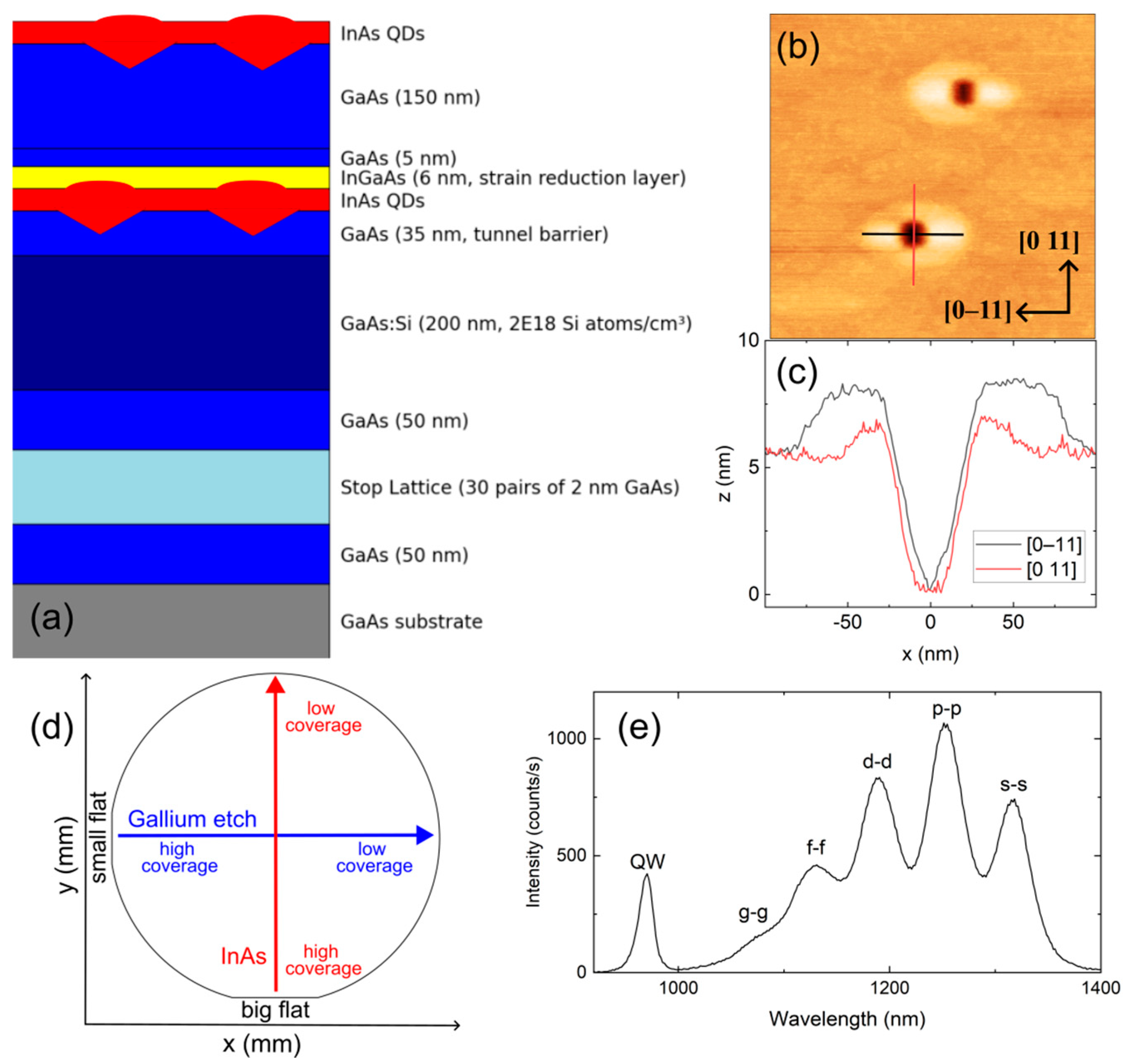
For all samples, the initial growth steps up to the optically active region were the same. As depicted in
Figure 1a, the typical layer structure of an LDE QD sample is shown. The standard QD samples share the same structural design, with the key distinction being the absence of LDE before the QD layer. The substrate temperature was lowered to 600 °C, followed by the growth of a 50 nm GaAs buffer layer. Subsequently, either a 2 nm GaAs stop layer or an AlAs/GaAs short-period superlattice was deposited, followed by a 10 s annealing pause to smooth the surface and serve as a buffer against impurities in the wafer. Another 50 nm of GaAs was then grown, followed by 200 nm of Si-doped GaAs (2 × 10
18 atoms/cm
3) and a 30 nm to 35 nm thick GaAs tunnel barrier to enable C-V spectroscopy measurements.
The process for LDE was initiated by decreasing the arsenic flux to a BEP of about 1.7 × 10
−7 Torr measured with a flux monitoring tube, and lowering the temperature to 530 °C. A four-minute stabilization break allowed for the flux, chamber pressure, and temperature to equilibrate. Gallium was then deposited as the etchant for the LDE process, equivalent to 3 ML GaAs, followed by a three-minute annealing break. Nanoholes formed by this method were characterized by AFM, as shown in
Figure 1b,c, displaying their shape and line profile. The arsenic BEP was then increased to 6.8 × 10
−6 Torr, and the temperature was lowered to 515 °C for InAs deposition.
InAs QDs were grown in cycles, with the shutter opened and closed at four-second intervals. We used 11–12 cycles for LDE QDs, while approximately 12–15 cycles were used for standard QDs. AFM measurements of the LDE QDs are presented in
Figure 2b and
Figures S1–S3. All QD growth was conducted partially without substrate rotation, resulting in a gradient in InAs material thickness. When rotation was halted, the indium cell was aligned towards the wafer’s big flat (BF), as shown in
Figure 1d. After InAs deposition, a 20-s break allowed for additional QD nucleation. The temperature was reduced by 50 K, and either a GaAs capping layer or a 6 nm InGaAs SRL was applied to samples targeting telecom O-band emission. A 5 nm GaAs layer was then deposited, and the temperature was increased to 590 °C with an arsenic BEP of 9.6 × 10
−6 Torr. A final 175 nm GaAs layer was grown before repeating the LDE and QD growth processes for the surface. A comprehensive overview of all samples is provided in
Table 1. Detailed growth protocols can be found in the
supplementary materials (see
Figures S4–S12).
Optical characterization was performed using a self-built PL spectroscopy setup capable of mapping the entire 3” wafer. The samples were cooled in a cryostat using liquid nitrogen, with all measurements conducted at approximately 80–85 K. Excitation was provided by a 516 nm laser, with a spot size of 100 µm in diameter and laser powers ranging from 2 to 5 mW. The PL spectrum of O-band QDs is shown in
Figure 1e. Based on their transitions, the ground and excited states are labeled as s-s, p-p, d-d, etc., and are subsequently referred to as s-, p-, and d-states or peaks. The emission of the quantum well (QW) formed with the SRL is labeled as QW.
For the C-V measurements, n-i-Schottky diodes were fabricated using 100 nm or 25 nm thick gold gates as Schottky contacts, with gate sizes of 300 × 300 µm
2 or 160 × 120 µm
2. The measurements were taken at 4.2 K. For C-V spectroscopy, a small AC signal (10 mV sine wave) is applied to the gate and superimposed on a DC voltage sweep. As the QDs come into resonance with the Fermi energy, tunnel processes occur, leading to the charging of QD levels with electrons. This charging is observed as changes in capacitance between the gate and the back contact. The gate voltage can be translated into energies
E(
UG) based on the lever arm [
26,
27], calculated using the following formula [
28]:
where
L1 is the thickness of the tunneling barrier,
L2 is the distance between the QDs and the gate,
e represents the elementary charge,
UG is the gate voltage, and
Ubi is the built-in voltage, with a value of 1.03 V in this work.
3. Results and Discussion
To shift the ground state emission of the QDs into the telecom O-band, the QDs were capped with 6 nm of In
0.3Ga
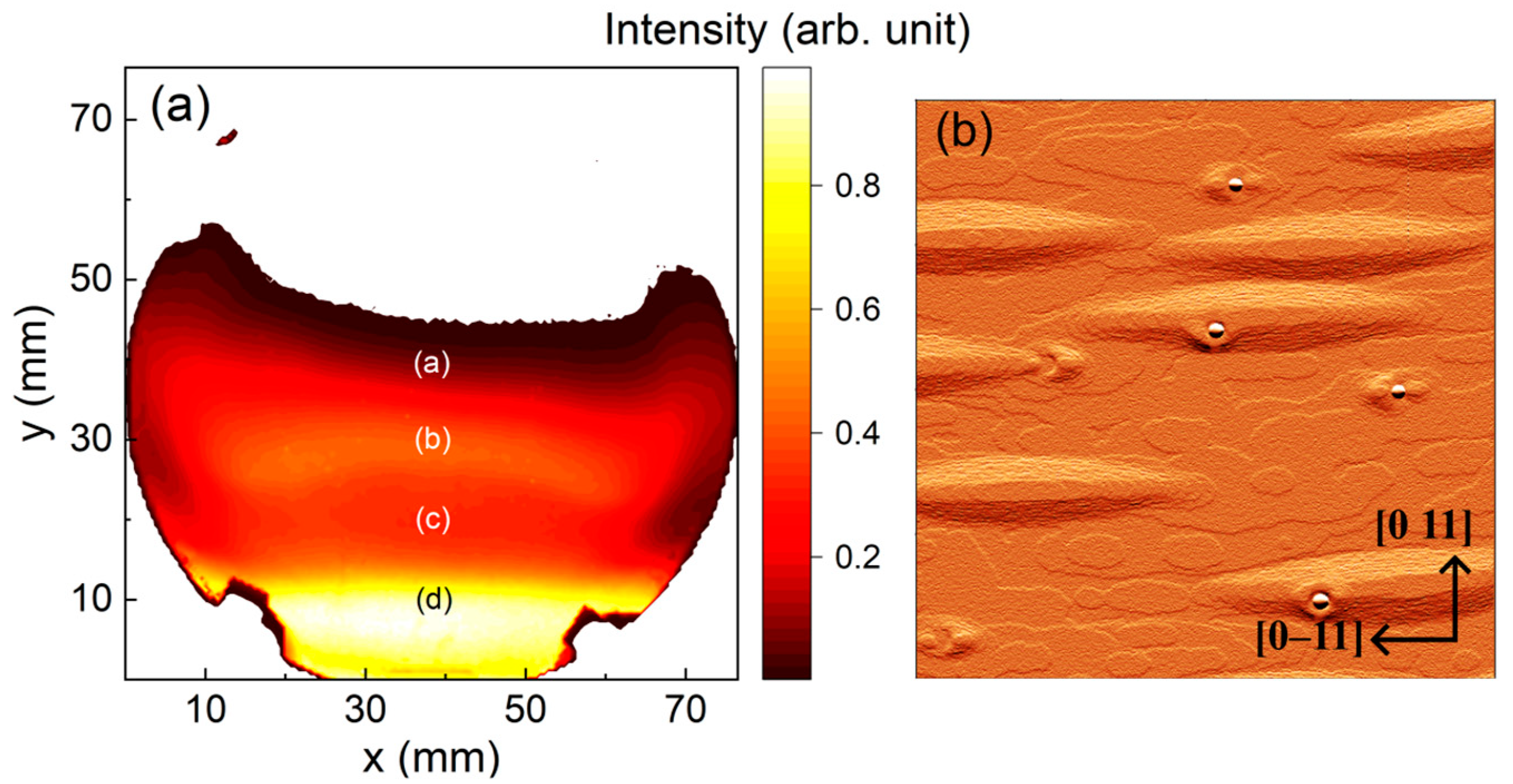
0.7As SRL instead of GaAs. The PL map of sample A
LDE, SRL, shown in
Figure 2a, displays the integrated spectrum over a wavelength range of 1000 nm to 1400 nm. The intensity is highest near the BF and decreases with distance, though not continuously. A notable dip in intensity occurs around y = 20 mm, where the intensity is lower than in the surrounding area, and sharp transitions in intensity are observed, such as at y = 10 mm.
Figure 3a–d shows the spectra from the corresponding positions highlighted in the PL map in
Figure 2a. At position (a), both the ground state and first excited state are visible, with the ground state emission at 1050 nm, which is not yet within the O-band. In contrast, the spectrum at position (b), located at coordinates (38|30), shows a ground state emission around 1150 nm with two excited states visible. This is attributed to the increased InAs deposition resulting from the material thickness gradient.
At position (c), the ground state emission reaches 1300 nm, which falls within the O-band. In this region, five distinct peaks can be seen, with the s- and p-peaks having a minimum full-width at half-maximum (FWHM) of 33 meV. The AFM image in
Figure 2b shows the surface in the region of the O-band QDs. The image displays QDs encircled by a ring, which is a clear indicator of SK growth within the nanoholes. Additional elongated mounds along the [0–11] direction represent buried QDs, useful for localization and processing. An analysis of further AFM images, which are listed in the
Supplementary Section (see
Figures S1–S3), shows that the density of buried and surface QDs is consistent.
At position (d), a significant change in the spectrum is observed, with a broader FWHM and fewer peaks. The s-s emission is at 1265 nm, and the separation between peaks increases, likely due to the critical layer thickness of approximately 1.5–1.7 ML of InAs being exceeded. This results in the nucleation of conventional SK QDs, which emit concurrently with the LDE QDs, thereby broadening the emission spectrum.
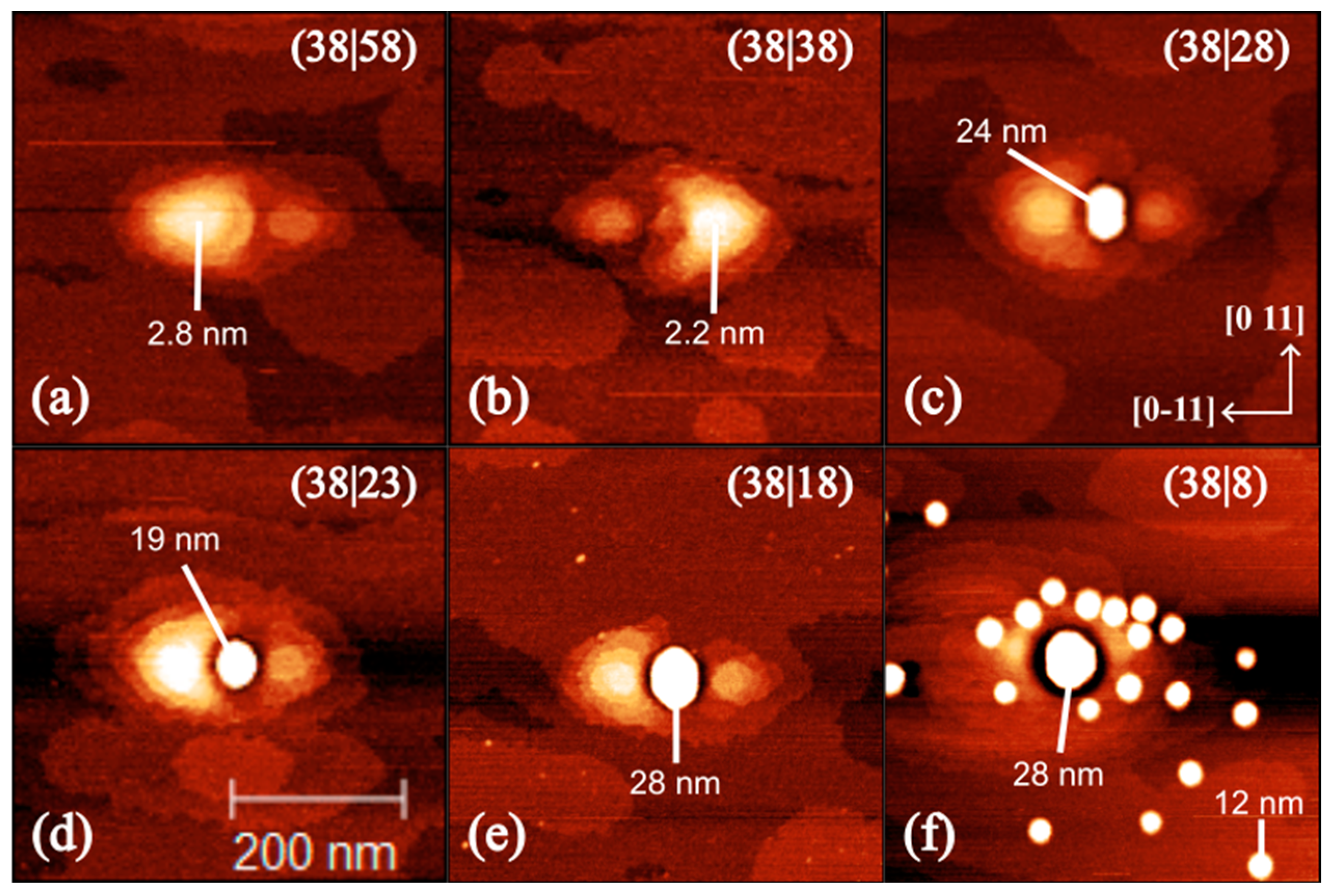
AFM images were taken of sample B
LDE, which had the same QD growth process on the surface as sample A
LDE, SRL. The optically active QDs in this sample were capped with GaAs, making them unobservable at the surface in contrast to sample A
LDE, SRL. Six AFM measurements, each 500 × 500 nm
2 in size, show individual QDs as can be seen in
Figure 4a–f. These images explain the differences in the spectra of
Figure 3a–d. Surprisingly, even in regions with the lowest amount of InAs deposited (around 1 ML), such as in
Figure 4a, the nanoholes are fully filled, leaving only a ring visible, elongated along the [0–11] direction. The high mobility and migration ability of indium atoms on GaAs and InAs surfaces [
29,
30] explain why the nanoholes are no longer visible, as they are filled by diffusion. PL measurements show a significant redshift in emission wavelength as y-values decrease, corresponding to an increase in the amount of InAs deposited in that direction. As a result, the QDs in this region exhibit a uniform size, as the nanoholes have been fully filled with material.
In contrast, positions between y = 18–28 mm displayed in
Figure 4c–e have sufficient InAs to nucleate QDs in the nanoholes, with critical layer thickness only reached within the holes. This induces SK growth exclusively within the holes. At position (e), the InAs deposition is sufficient to form “predots,” small white features with a height of 1–2 nm, which eventually develop into larger QDs with additional indium deposition. The shape and size of the QDs change noticeably across these positions, with heights ranging from about 20 nm in (d) to 28 nm in (e). There are also significant differences in QD shape, with those in (c) and (e) being asymmetric. This suggests there is an optimal InAs amount for maximizing QD symmetry and homogeneity, particularly in the area around (d), confirmed by PL measurements in
Figure 3c and
Figure 5, where numerous clearly separated peaks indicate high homogeneity.
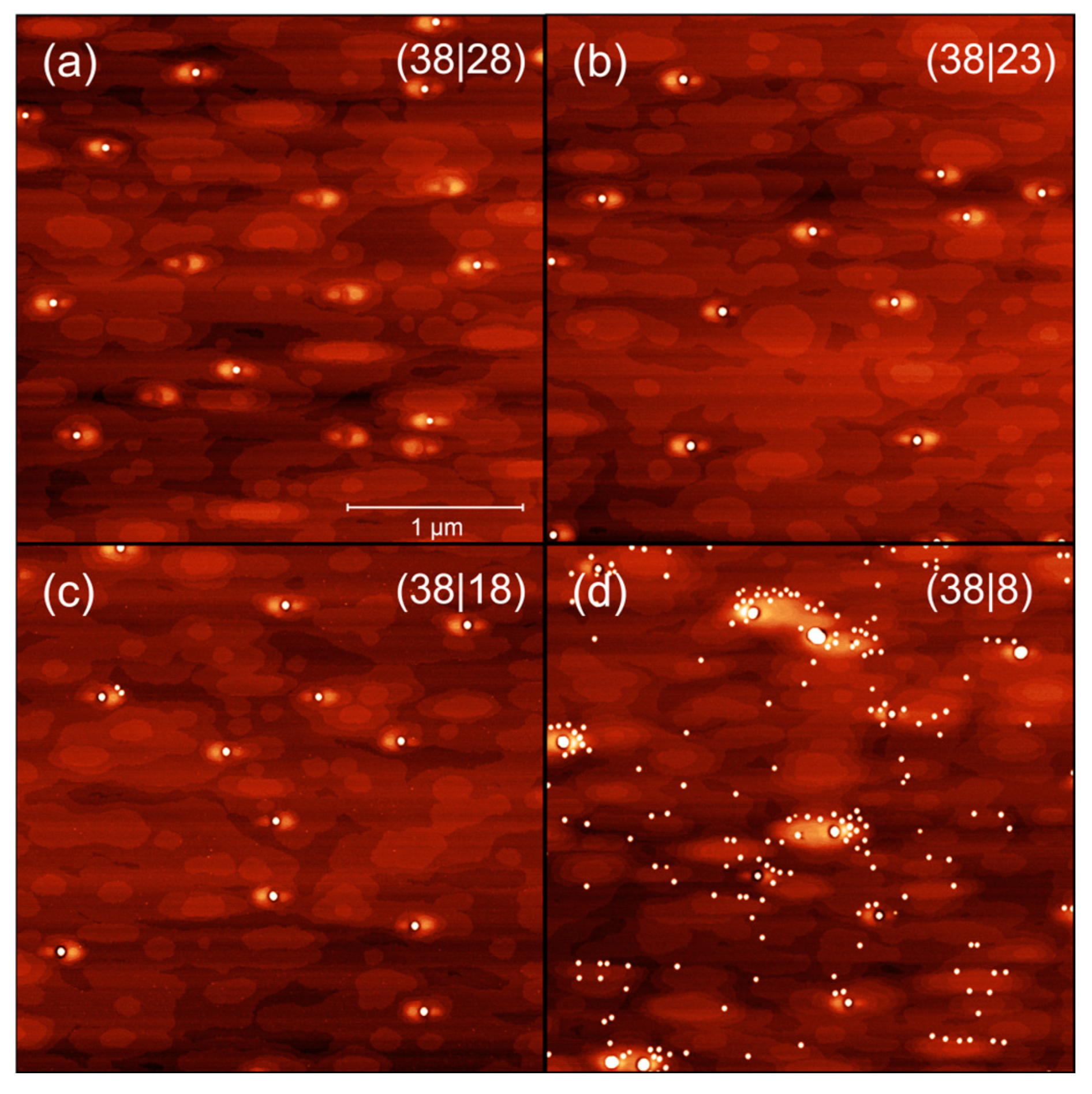
A statistical analysis of QD sizes was performed based on 3 µm x 3 µm AFM images in
Figure A1 in the
Appendix A. The average heights of the LDE QDs at each position are as follows: (38|28) (13.6 ± 3.6) nm, (38|23) (18.3 ± 1.4) nm, (38|18) (19.5 ± 2.7) nm, and (38|8) (24.6 ± 7.8) nm. These results clearly indicate that QD size is strongly influenced by the amount of deposited InAs. Notably, with an uncertainty of ±1.4 nm, the QDs at position (38|23) (also shown in
Figure 4d) exhibit the lowest height variations, indicating particularly high uniformity.
In regions where the InAs amount exceeds 1.5 ML, as seen in
Figure 4f, QD nucleation occurs outside of the nanoholes. This accounts for the increased intensity observed in region (d) of the PL map shown in
Figure 2a and the corresponding spectral changes illustrated in
Figure 3d. The QDs tend to align around the nanoholes, likely due to higher indium concentration in these areas and an increased number of step edges [
31]. PL measurements in
Figure 3d indicate that the large QDs within the nanoholes are no longer optically active. Based on their size and height, one would expect them to emit in the O-band or beyond; however, no emission is observed in this wavelength range. This could suggest that the QDs have exceeded a critical size, where excessive strain or even dislocations prevent optical emission.
Figure 5 shows the waterfall plot of the PL spectra for sample A
LDE, SRL, recorded along the InAs gradient at position x = 38 mm, within the range where LDE QDs are expected. Between the coordinates 20 mm and 25 mm, the spectra remain nearly identical despite the presence of the gradient, suggesting that QD growth within this region has entered a parameter window where highly similar QDs are consistently formed. Beyond 25 mm however the peaks shift strictly monotonically towards shorter wavelengths, eventually becoming indistinguishable from the InGaAs QW emission caused by the SRL that caps the QDs. Notably, the ground state emission wavelength shifts from approximately 1300 nm to 1050 nm in a narrow range of only 15 mm on the wafer.
Studies have demonstrated similar shifts in QD emission wavelengths [
32]; however, with this new method, it is now possible to achieve such a broad spectral range on a single wafer. By progressively filling the nanoholes with InAs, the gradient growth results in significant variations in the size of the quantum dots. This tunability highlights a key advantage of LDE QDs: the emission energy can be easily adjusted over a wide range.
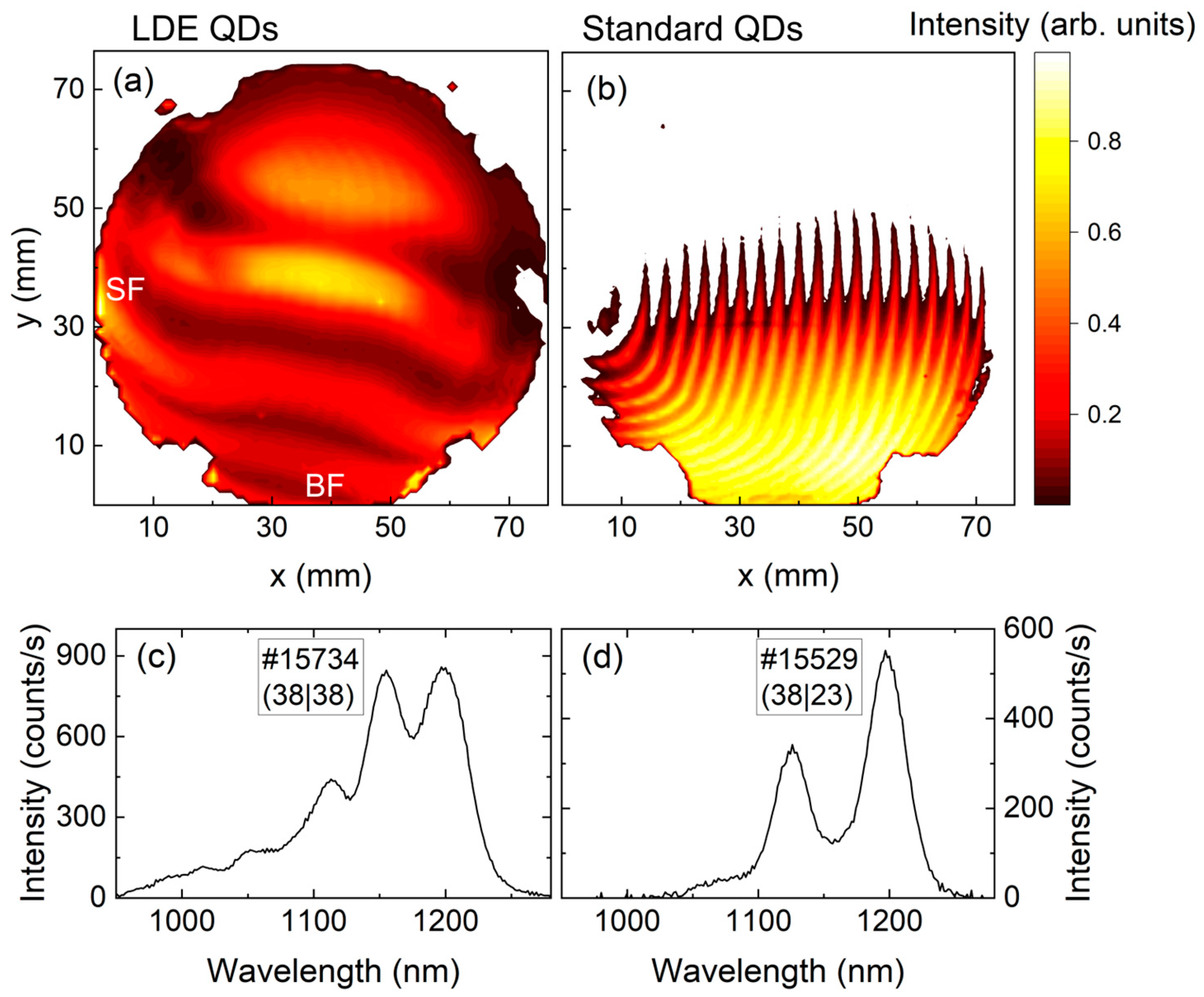
In
Figure 6, the PL spectra for samples C
LDE, PDL (LDE QDs) are displayed in panels (a) and (c), while panels (b) and (d) show the measurements for D
St, SRL (standard QDs). The GaAs layer beneath the QDs was grown without wafer rotation, leading to a material thickness gradient, referred to as a pattern definition layer (PDL) which modulates QD density on the wafer [
33]. Rougher surfaces increase the likelihood of QD nucleation, compared to atomically smooth surfaces. During layer-by-layer growth, atomically flat substrates experience cycles of roughening and smoothing as the fractional completion of each monolayer changes. When a monolayer is complete, the surface roughness is minimized, while non-integer layer coverage increases atomic roughness. This characteristic is used in reflection high-energy electron diffraction growth rate analysis, a common technique in MBE.
We exploit the effect of surface roughness on QD nucleation by growing thickness gradients, known as the PDL [
33], before QD formation. This process introduces controlled in situ transitions between integer and non-integer atomic layer completions, resulting in modulated surface roughness. By orienting the substrate relative to the gallium effusion cell—specifically pointing it toward the small flat—we can precisely control the surface roughness profile. This adjustment facilitates the formation of crescent shaped QD density patterns across the wafer, as illustrated in
Figure 6a,b. The wafer maps illustrate the integrated intensity of the QD emissions in the wavelength range of 950 nm to 1300 nm, with representative spectra embedded for both samples. Both samples contain InAs QDs embedded in a GaAs matrix, with the InAs deposited using the gradient method, starting from the BF.
For sample CLDE, PDL, the effects of the PDL on the emission intensity are minimal, whereas in sample DSt, SRL, the influence of the PDL is clearly visible, significantly affecting the intensity. Another notable difference between the two samples is the position of the maximum intensity. For sample CLDE, PDL, it is found in the middle of the wafer, whereas in sample DSt, SRL, it is located near the BF, which is attributable to the amount of deposited InAs.
A comparison of the spectra from both samples, shown in (c) and (d), reveals that the energy separation between the s- and p-states differs. For the LDE QDs in sample CLDE, PDL, the energy difference is 42 meV, while for the standard QDs in sample DSt, SRL, it is 66 meV. However, the FWHM values are comparable, at around 35 meV. Additionally, more excited states are visible in sample CLDE, PDL, though differences in QD density and laser power make direct comparison difficult.
The smaller energy separation between the s- and p-states in the LDE QDs could be attributed to two mechanisms. The first is interdiffusion during and after nucleation, which leads to a higher gallium content within the QDs [
34]. The second is the larger volume and height of the QDs, both of which contribute to the reduced energy separation [
34,
35]. It is also possible that a combination of these two factors is responsible. A larger QD volume results in a stronger oscillator strength, leading to improved quantum efficiency [
36,
37]. Additionally, larger QDs tend to exhibit smaller fine-structure splitting [
38], a crucial property for their use as single-photon sources.
Figure 7 presents the PL measurements of two samples that were produced under identical conditions, except for the QD growth method, and grown on the same day to ensure optimal comparability. The QDs in sample E
LDE, SRL were grown using the novel LDE method, whereas sample F
St, SRL used the standard method.
Figure 7a,b show wafer maps illustrating the ground state emission wavelength, with the data derived from Gaussian fits to the s-peak. Plot (a) shows pronounced differences in the ground state emission wavelength along the
y-axis, ranging from 1000 nm to 1320 nm. In the red region between y = 20 mm and 27 mm, only homogeneous LDE SK QDs emitting in the O-band are found. Sharp boundaries above and below this area show abrupt shifts in emission energy. Below this area, QDs nucleate outside of the nanoholes, while above it, the QD size progressively decreases until the filling of nanoholes occurs in the Frank–Van der Merwe growth mode, as the indium amount further decreases.
While sample ELDE, SRL displays a modulation in emission wavelength in the lower region up to y = 15 mm, reaching its maximum redshift at y = 20 mm before subsequently decreasing, the reference sample FSt, SRL, shown in Plot (b), exhibits a wavelength modulation that varies between 1230 nm and 1310 nm. This variation is attributed to the cyclic deposition of InAs during QD growth. These effects are caused by the cyclic deposition of InAs with halted rotation, leading to different maturation behaviors of the QDs. In each cycle, the amount of InAs gradually increases until nucleation occurs near the BF. The density of this initial QD generation decreases from the BF onwards, until it reaches a point where the amount of InAs is just enough for SK growth. At this transition, the QD density reaches a minimum and drops to zero in more distant regions.
In the following cycle, when additional InAs is deposited, the extra material distributes across regions of lower density over fewer QDs compared to the underlying region with higher density. The QDs in the low-density regions have larger Voronoi cells and can thus incorporate more indium, causing them to grow larger. The differences in density remain intact. Consequently, in each generation, there is a gradual transition from blue-shifted QDs with high density to red-shifted QDs with low density. After the initial nucleation, each new cycle shifts the transition where no QDs are present further out, effectively creating a new generation of QDs. This again leads to a gradient from high to low density. These various QD generations result in a modulation of emission energy and wavelength [
39].
Figure 7c,d displays heatmaps of the PL intensity along the
y-axis at an x-position of 38 mm. A key feature is the position of the InGaAs-QW, which provides insights into the width and composition of the QW layer, functioning as an SRL. The LDE sample emits at around 950 nm, while the QW of the standard sample emits at approximately 980 nm. Both SRLs have a width of 6 nm; however, as shown in
Table 1, the LDE sample required less indium to reach the O-band. This reduction in indium is advantageous as it minimizes strain within the sample.
The spectra of both samples are displayed in
Figure 7e,f. The energy difference between the s- and p-peaks is smaller for the LDE sample, with the energy difference for sample F
St, SRL being 60 meV, while for sample E
LDE, SRL, it is reduced to 47 meV.
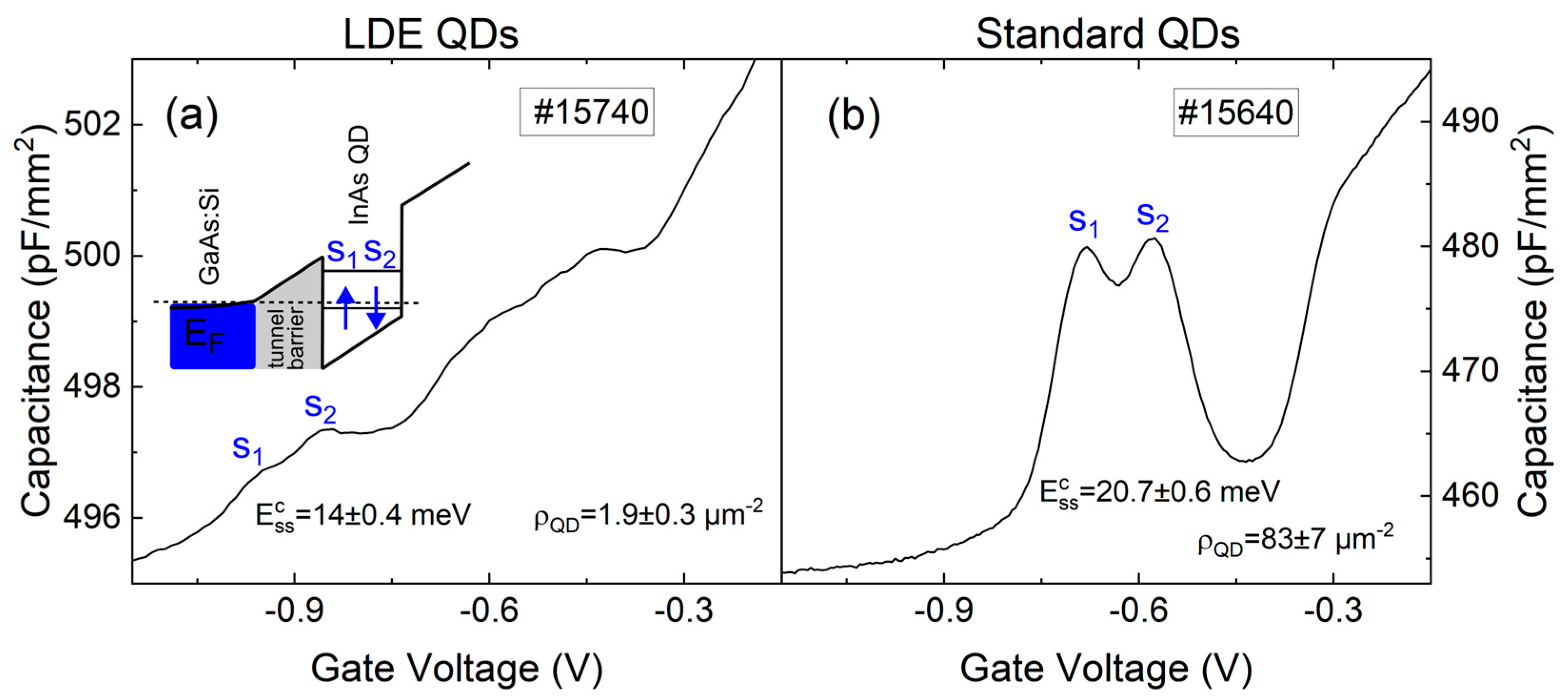
C-V measurements were conducted on both LDE QDs (sample A
LDE, SRL) and standard QDs (sample G
St, SRL, PDL), as shown in
Figure 8. Both samples emit in the O-band. The measurements were normalized by dividing the capacitance by the gate area due to the different gate sizes used. The peaks corresponding to the s
1 and s
2 charging events are labeled. The inset in plot (a) illustrates the charging process: the s1-peak corresponds to single electron charging of the QDs below the gate and the s2-peak to second electron charging. This second charging takes place at the same orbital but with opposite spin due to the Pauli principle.
Due to Coulomb blockade, a higher gate voltage is required for the tunneling of the second electron [
40]. The Coulomb blockade energy is related to the size of the quantum dots, with smaller dots exhibiting stronger Coulomb repulsion. Based on the measured Coulomb blockade energies, LDE QDs exhibit a value of 14 meV, indicating they have a larger lateral wavefunction than the standard QDs, which exhibit a higher Coulomb blockade energy of 20.7 meV in accordance with the larger level splitting observed above.
The difference in the magnitude of the s
1-peak between the two samples is attributed to a different QD density
ρQD. In sample (a) and (b), we find a density of 1.9 µm
−2 and 83 µm
−2, respectively. The density of the LDE sample is in good agreement with the surface LDE nanohole density. The density of QDs, obtained by subtracting the diode background from the capacitance and factoring in the twofold degeneracy of the lowest orbital energy states [
28], is provided by the following:
represents the lever, calculated as , where is the tunneling barrier thickness, and is the distance between the QDs and the gate. Additionally, denotes the elementary charge, the gate surface area, the subtracted capacitance, and the applied DC gate voltage.
The effects of the indium flush method on both types of QDs were investigated by comparing samples I
St, Flush and H
LDE, Flush. Sample H
LDE, Flush was fabricated using the LDE method under similar conditions to sample C
LDE, PDL, with the key difference being that the QDs were covered with 3.5 nm of GaAs before applying the indium flush technique. Sample I
St, Flush, on the other hand, was grown using the standard method and then modified with the flushing procedure with nominally 3.5 nm GaAs capping height, as described in more detail in [
17].
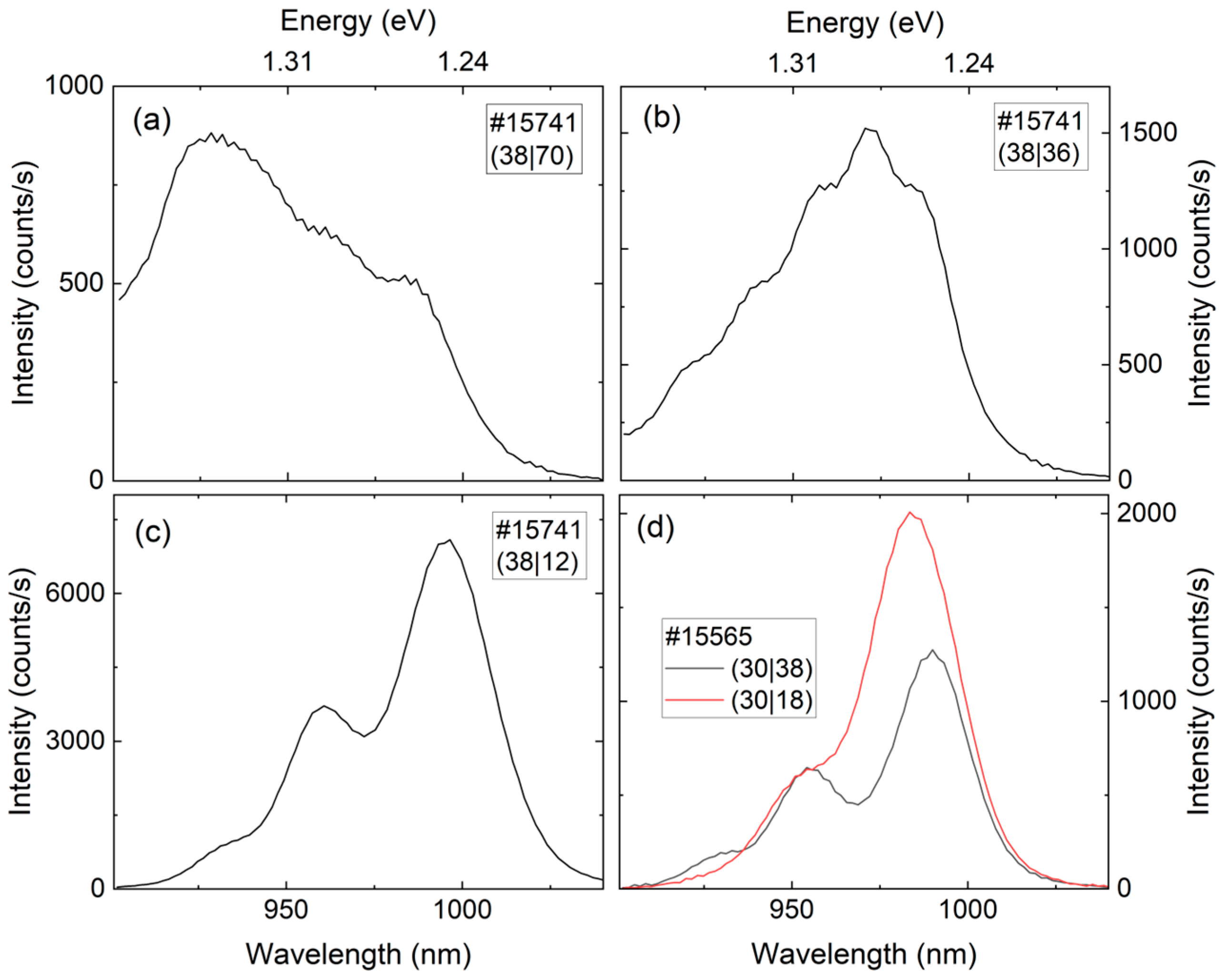
The PL spectra of both samples are compared in
Figure 9, where positions for sample I
St, Flush were selected to match the GaAs coverage of H
LDE, Flush. The indium flushing process resulted in varying outcomes for the LDE sample depending on the position, as can be observed in spectra (a), (b), and (c), which show significant differences. In all three cases, the ground-state wavelength is around 990 nm. This result was expected at positions (b) and (c), where SK QDs are present, as the In-flush technique adjusts the QD height to the GaAs coverage thickness.
However, at position (a), Frank–Van der Merwe growth occurs, as evident from the AFM images in
Figure 4a,b. Surprisingly, a similar emission wavelength is also achieved at this position, despite the different growth mode. Further investigation is needed to determine whether this is coincidental or if the ring or wall surrounding the nanohole is optically active in this region. At position (38/12) (cf.
Figure 9c), QDs nucleate outside of the holes, resulting in a spectrum similar to that of position (30/38) and (30/18) of sample I
St, Flush (cf.
Figure 9d).


 ,
, 


