Article

High-Performance Broadband Photodetectors Combining Perovskite and Organic Bulk Heterojunction Bifunctional Layers

State Key Laboratory of Dynamic Measurement Technology, North University of China, Taiyuan 030051, China
*
Authors to whom correspondence should be addressed.
Crystals 2024, 14(10), 868; https://doi.org/10.3390/cryst14100868
Submission received: 11 August 2024 / Revised: 9 September 2024 / Accepted: 25 September 2024 / Published: 1 October 2024
(This article belongs to the Section Organic Crystalline Materials)

Abstract

:
Perovskite can be used to prepare high-performance photodetectors due to its excellent optical properties. However, the detection range of perovskite photodetectors is mostly limited to the visible light range, restricting their further development and application. In recent years, combining perovskite with organic bulk heterojunctions to prepare photodetectors with broadband detection capability has proven to be an effective strategy. Through this approach, the response spectrum of the photodetector can be flexibly regulated, and organic compounds can improve the perovskite film quality by passivating defects and inhibit the penetration of water molecules in the air, thereby improving the device performance and stability. In this work, we propose and demonstrate the feasibility of combining MAPbI3 perovskite with PTB7-Th:COTIC-4F to prepare high-performance photodetectors with wide spectral response characteristics. With the assistance of an organic bulk heterojunction, the defects of perovskite crystals are effectively passivated, and the detection spectrum of the device is successfully extended to about 1100 nm. As a result, the responsivity achieved is 0.58 A/W, 1.19 A/W, and 1.41 A/W under laser illumination of 532 nm, 808 nm, and 980 nm, with the power density of 5 μW/cm2 at the bias voltage of −0.5 V, respectively, which is one of the best performances among vertical device structures of this type. Moreover, the stability of the final hybrid film has been greatly improved. This work provides a new approach to the preparation of high-performance and broadband perovskite photodetectors.

1. Introduction

Photodetectors (PDs), which can convert optical signals into electrical ones, have achieved widespread attention and applications in emerging fields such as autonomous vehicles, machine vision, artificial neural networks, and biometric identification [1,2,3,4,5]. Recently, PDs based on organic–inorganic hybrid perovskite material have largely compensated for the shortcomings of traditional inorganic PDs owing to their inherent advantages, such as facile solution processes, low-cost manufacturing, adjustable optoelectronic properties, and compatibility with flexible substrates, becoming emerging candidates for next-generation high-performance PDs [6,7,8,9]. However, despite perovskite PDs having made remarkable progress, the shortcoming of the detection region being limited to the visible range cannot be ignored. In the face of the rising demand for near-infrared (NIR) detection in medical monitoring, quality monitoring, and bioimaging, the methylammonium lead halide (MAPbX3, X is Cl, Br, I) perovskite has considerably constrained roles in the NIR region due to its relatively large bandgap [10], which seriously hinders the progress of perovskite PDs towards use in commercial applications. To overcome this issue, low-bandgap perovskite materials have been exploited in component engineering to achieve an extended absorption range covering NIR light [11,12,13,14]. For instance, the bandgap of ABX3-type perovskite materials can be reduced by introducing FA+ cations at the A-site cations or Sn2+ cations at the B-site cations in the lattice, corresponding to the extension of the light response up to 1100 nm [15,16]. Nevertheless, these low-bandgap perovskites are typically surrounded by practical issues including poor stability and low performance [17,18]. Therefore, it is essential to find a simpler and more feasible strategy to significantly broaden the NIR absorption spectrum of devices for the advancement of PDs.
In recent years, the strategy of integrating perovskite into an organic bulk heterojunction (OBHJ) have been shown to allow the successful construction of broadband-detected PDs [19,20]. Firstly, this combination provides great flexibility to design and manipulate the spectral detection window. Secondly, the bulk heterojunction can effectively facilitate carrier separation, reducing dark current and improving light current, thus leading to high sensitivity and a fast response. Thirdly, the organic compounds can passivate defects in the perovskites and protect perovskites from external invasions (H2O, O2, etc.), enhancing device performance and stability. Finally, the common advantages, such as low cost, tunable bandgap, excellent mechanical flexibility, and facile solution processibility, offer enormous potential in next-generation portable and wearable PDs [21,22,23,24]. Wu et al. introduced NIR-sensitive PTB7-Th:IEICO-4F with MAPbI3 (PVK) film in the integrated PD and elevated the highest responsivity of 0.444 A/W and 0.518 A/W in the visible and NIR region, respectively [25]. However, due to the solvent orthogonality with OBHJ, the presence of PC61BM more or less affects the contact between PVK and OBHJ, further affecting the performance of the device. Li et al. prepared PDs with a broadband response spectrum of up to 1000 nm by combining PVK and F8IC:PTB7-Th in a rational design, and the corresponding responsivity peaks reached 0.37 A/W and 0.43 A/W in the visible and NIR region, respectively [26]. Luong et al. proposed highly sensitive organic PDs with a PTB7-Th:COTIC-4F blend system as the active layer to achieve shortwave infrared sensing, and the corresponding responsivity peaks reached 0.52 A/W in the NIR region. However, the performance of the devices in the NIR region is much lower than that of the devices composed of a single active layer of PVK, indicating that the selection of the NIR-sensitive layer in the device still needs to be more considered [27]. In terms of material selection and structural design, the challenge is how to select suitable NIR-sensitive OBHJ materials to avoid mismatch between the energy levels of perovskite and the OBHJ layer. On the other hand, the interfacing contact between perovskite, OBHJ, and corresponding charge transport materials should be improved to favor the efficient extraction and transport of the photogenerated charge carriers in between layers of perovskite and OBHJ in both the visible and NIR regions.
In this study, we proposed and demonstrated a new scheme to combine PVK polycrystalline film with PTB7-Th:COTIC-4F bifunctional OBHJ to achieve not only the excellent passivation of crystal defects in perovskite layers but also highly sensitive detection covering visible-to-NIR light. As a result, the PD based on MAPbI3/PTB7-Th:COTIC-4F (PVK/OBHJ) material achieved the high responsivity of 0.58 A/W, 1.19 A/W, and 1.41 A/W and the high specific detectivity of 1.64 × 10¹² Jones, 3.32 × 10¹² Jones, and 3.87 × 10¹² Jones under illumination of 532 nm, 808 nm, and 980 nm lasers with the power density of 5 μW/cm2 at bias voltage of −0.5 V, respectively. Moreover, the stability of the final hybrid film has been greatly improved. This study provides a new cost-effective alternative for the preparation of broad-spectrum and high-performance perovskite PDs.

2. Materials and Methods

2.1. Material Preparation

Lead iodide (PbI₂, purity over 99.99%) and methylammonium iodide (CH₃NH₃I, also known as MAI, purity over 99.5%), poly(3,4-ethylenedioxythiophene)/polystyrene sulfonate (PEDOT:PSS), fullerene (C60, purity over 99%), and Bathocuproine (BCP, >99%) were all purchased from Xi’an Yuri Solar Co., Ltd. (Xi’an, China). PTB7-Th and COTIC-4F were purchased from Solarmer Materials Inc. (Beijing, China). N,N-dimethylformamide (DMF, purity over 99.5%), dimethylsulfoxide (DMSO, purity over 99.5%), and sec-butanol alcohol (SBA) were all purchased from Aladdin. All chemicals were used without further purification.

2.2. Device Fabrication

The pre-patterned glass/ITO substrates were first cleaned ultrasonically, in the order of glass cleaner, deionized water, acetone, and isopropanol, and then post-treated with an ultraviolet ozone cleaner for 15 minutes to enhance their wettability. The PEDOT:PSS solution was spin-coated on top of the cleaned ITO substrates at 4000 rpm for 40 s, followed by annealing at 150 °C for 15 minutes. The preparation of the active layers was carried out in a glove box filled with nitrogen, which ensured that the preparation process of perovskite thin films effectively avoided the influence of environmental factors such as water and oxygen. The PVK solution was prepared by dissolving PbI2 and MAI with a molar ratio of 1:1.05 in the mixed solvent of DMF and DMSO with a volume ratio of 9:1 and stirring overnight at room temperature. Then, 100 μL perovskite precursor solution was spin-coated on the PEDOT:PSS substrate at 6000 rpm for 30 s, and 265 μL of the SBA antisolvent was slowly dropped on the wet film at about the 7th second during the spin-coating process. Subsequently, the samples were rapidly moved to a hot plate, first annealed at 100 °C for 20 min, and then annealed in a DMSO atmosphere at 100 °C for 10 min. The blend solution (total concentration of 20 mg/mL) of PTB7-Th (1.0 wt%):COTIC-4F (1.5 wt%) dissolved in chlorobenzene with 2 vol% 1-chloronaphthalene (CN) was spin-coated on top of the PVK layer at 3000 rpm for 30s and then annealed at 80 °C for 20 min. C60 and BCP were sequentially transferred to the organic bulk heterojunction layer by vapor deposition and spin coating processes. Finally, the devices were completed by evaporating a 5 nm thick Cr and an 80 nm thick Au electrode.

2.3. Characterization

The cross-sectional images and the surface morphologies of the different perovskite films were characterized using SEM (HITCHI SU8020, Tokyo, Japan) and AFM (CSPM5500, Guang Zhou, China). Absorption spectra of the thin films were obtained using a Shimadzu UV-2600 spectrophotometer (Kyoto, Japan). XRD measurements of the perovskite films were performed with a Rigaku D/MAX-2500 diffractometer (Akishima, Japan). Steady-state and time-resolved photoluminescence spectra were measured using an Edinburgh FLS 1000 fluorescence spectrophotometer (Edinburgh, Britain). The I-V characteristics of all PDs under 532 nm, 808 nm, and 980 nm laser illumination were recorded using a Keithley 2400 source meter instrument (Cleveland, OH, US).

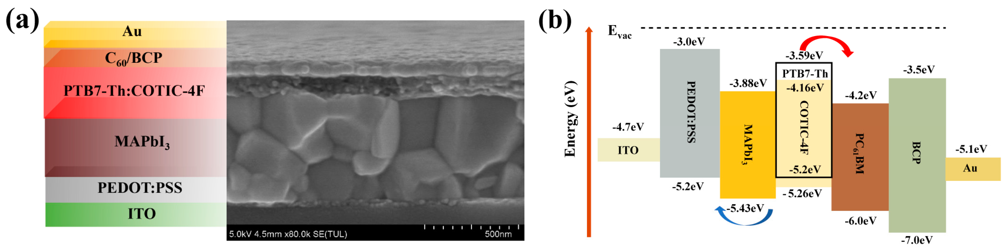
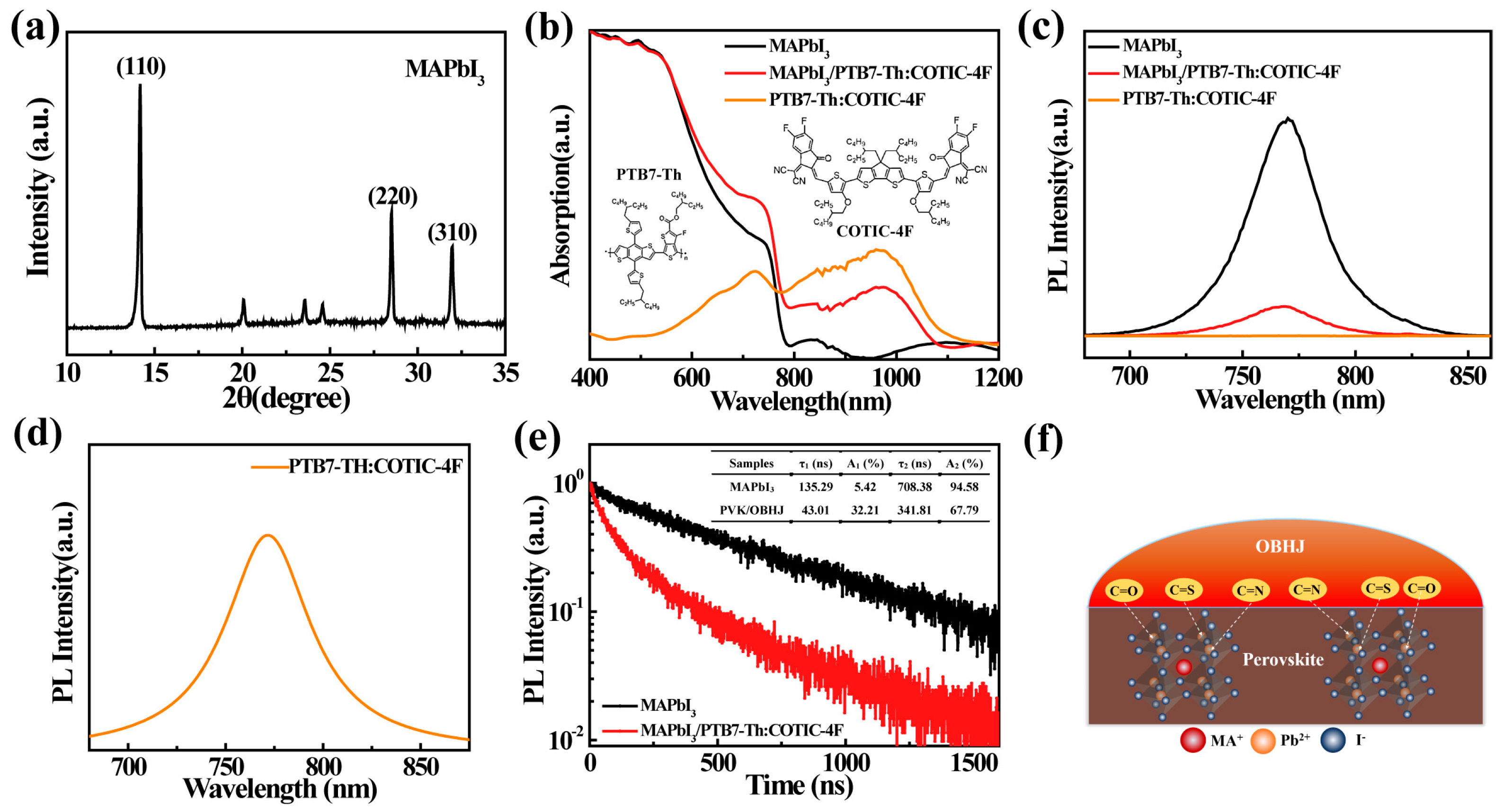
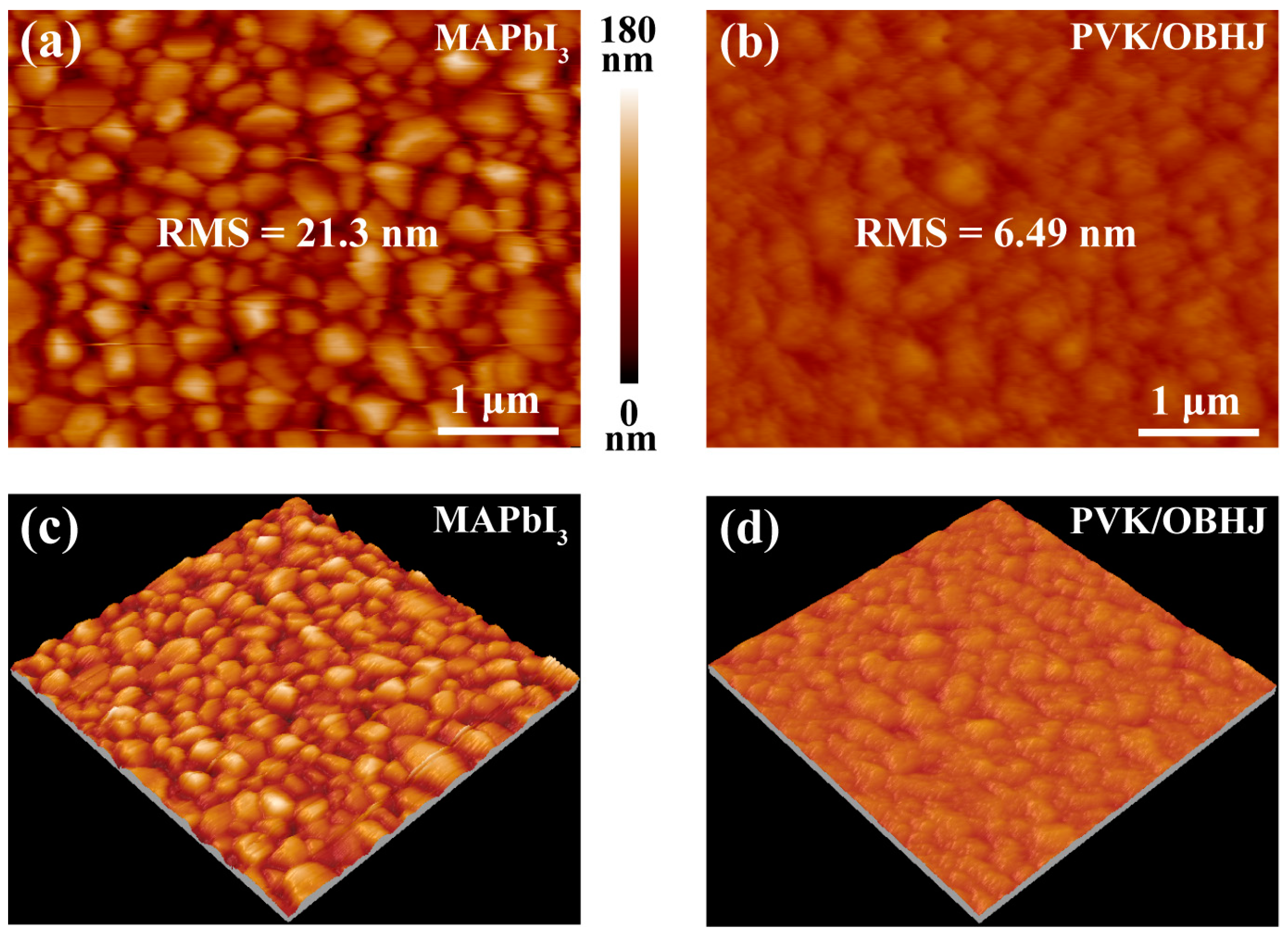
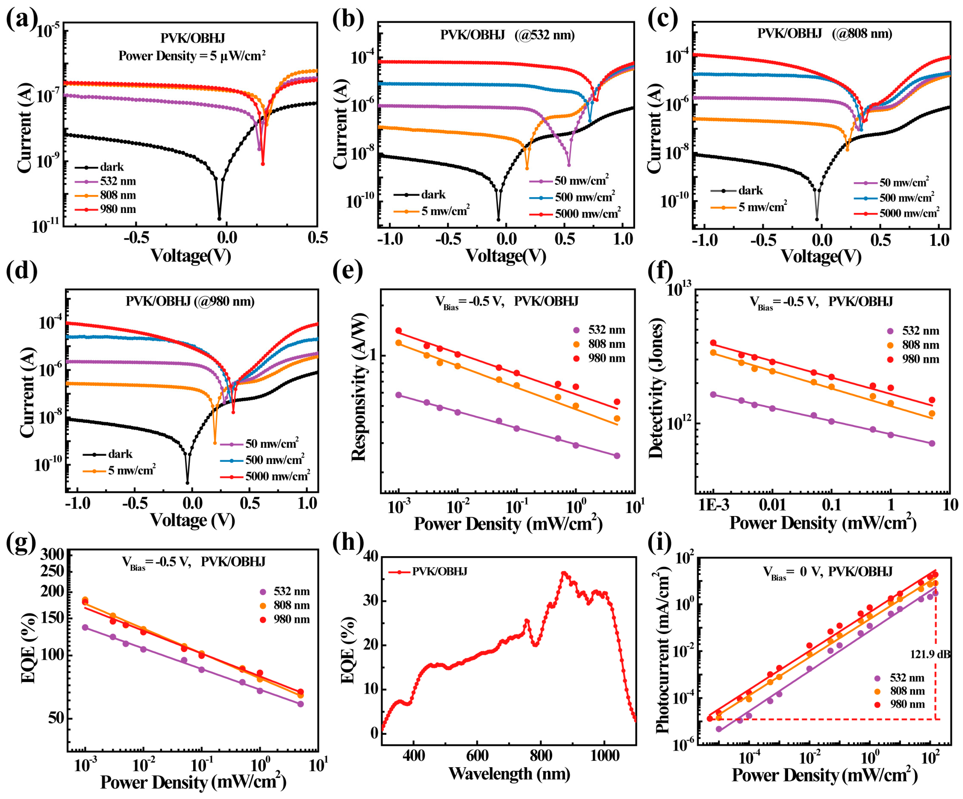
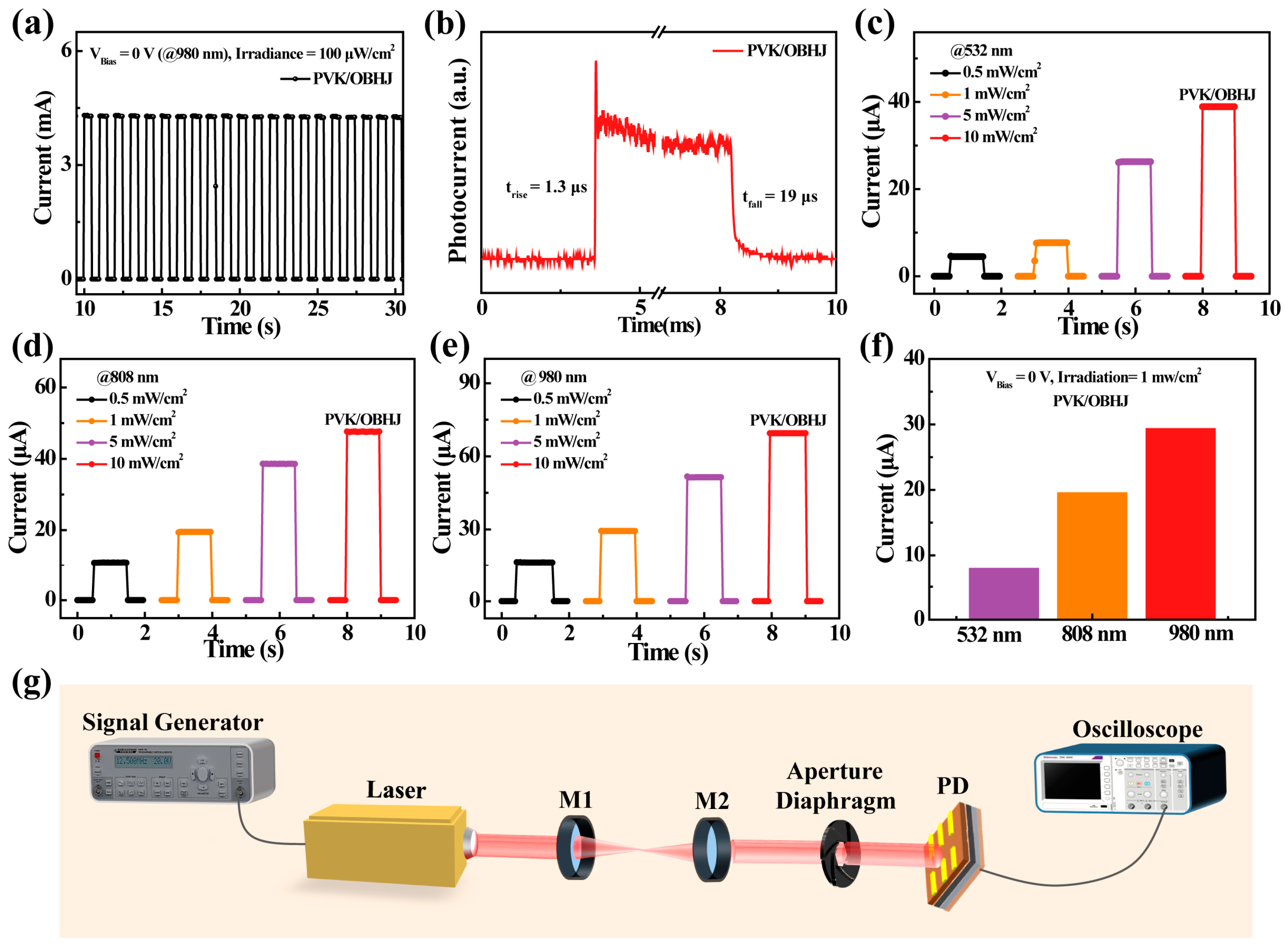
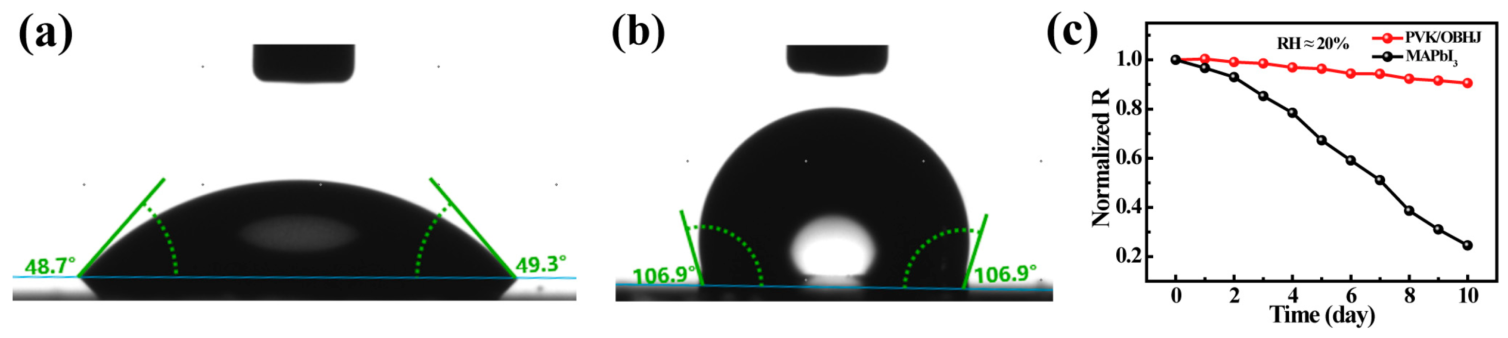
3. Results and Discussion

Figure 1a shows the schematic structure of the PVK/OBHJ-PD and the corresponding cross-sectional SEM image, where indium tin oxide (ITO) and gold (Au) act as anode and cathode, poly(3,4-ethylenedioxythiophene) polystyrene sulfonate (PEDOT:PSS) and fullerene C60/bathocuproine (C60/BCP) bilayers act as hole transport layer and electron transport layer, respectively, and PVK and OBHJ located in the middle layer of the structure are used as the core sensitive materials of the device. It can be clearly seen from the cross-sectional SEM image that the OBHJ layer is uniformly deposited on the PVK layer. The device energy band alignment diagram is elucidated in Figure 1b. The photoexcitons generated from the photon energy absorbed by the OBHJ layer can be effectively separated into free carriers with the assistance of the interpenetrating network structure formed by the heterojunction, in which the electrons are transported towards the Au electrode under the effect of the built-in electric field and the applied bias voltage, and the holes are transported to the ITO electrode through the perovskite layer and collected. The photogenerated electrons generated in the perovskite are transported to the Au electrode through the OBHJ layer, and the photogenerated holes are transported to the ITO electrode. It is worth noting that the presence of the OBHJ layer will have a good passivation effect on any defects at the interface, thereby reducing the interface carrier recombination.
In order to further understand the characteristics of the PVK, OBHJ, and PVK/OBHJ composite films, thereby revealing the mechanism of the effect of OBHJ on PVK, we analyzed their optical properties. Figure 2a plots the X-ray diffraction (XRD) pattern of MAPbI3 film. Three typical diffraction peaks are located at 14.17°, 28.51°, and 32°, corresponding to the (110), (220), and (310) crystal planes, respectively, indicating the great crystallinity of PVK film. Figure 2b depicts the absorption spectra of pure PVK, OBHJ, and PVK/OBHJ composite films and the chemical structures of PTB7-Th and COTIC-4F. Notably, the PVK film exhibits strong absorption across the entire visible spectrum, with an absorption cut-off edge around 780 nm. Although the OBHJ film shows certain light absorption characteristics in the range of 400~1100 nm, the absorption intensity is relatively weak in the range of 400~700 nm, whereas the PVK/OBHJ composite film combines the advantages of both the PVK film and the OBHJ film, achieving strong complementary light absorption in the range of 400~1100 nm. Steady-state photoluminescence (PL) and time-resolved photoluminescence (TRPL) spectra represent crucial techniques for characterizing film quality and assessing relative nonradiative charge carrier losses [28,29], and all the films were spin-coated onto bare glass substrates in this work. As shown in Figure 2c,d, the PL intensity of the PVK/OBHJ film is significantly lower than that of the PVK film, accompanied by a gradual blue shift of the emission peak position from 770 to 767 nm, which can be attributed to the rapid transfer of photogenerated carriers produced in the perovskite film to OBHJ film, and the presence of OBHJ layer effectively passivates the defects of perovskite films, thereby reducing interface trap recombination. The TRPL decay curves displayed in Figure 2e further validate this result, with detailed data provided in the embedded table. The PL lifetime associated with carrier recombination in the PVK film is 708.38 ns, while the corresponding lifetime in the PVK/OBHJ film is 341.81 ns, indicating that the charge carriers are successfully transferred to the OBHJ layer, which is crucial for improving the performance and response time of the detector. Figure 2f illustrates the passivation mechanism of the perovskite layer by the OBHJ layer. The thermally instable PVK loses methylammonium iodide and decomposes into PbI2 during the high-temperature treatment process in thin film preparation, accompanied by the generation of some uncoordinated Pb2+, which are considered as the main electron trap state and further limit the device performance. The electron-rich π-conjugated Lewis base groups in the OBHJ can effectively passivate the poorly coordinated Pb2+ in PVK by the coordination of Lewis acid and base, which promotes the carrier extraction and transfer process and reduces the charge carrier loss occurring at the interface, thus improving the device performance [30].
Based on the analysis of the optical characteristics of the aforementioned different films, we conclude that the presence of the OBHJ layer can effectively passivate the surface defects of the PVK film and thereby improve the film morphology. In order to obtain the surface morphology information for the PVK and PVK/OBHJ films more intuitively, we tested the surface AFM images of the two films. As shown in Figure 3a,b, the surface roughness of the PVK film is 21.3 nm. With the addition of the OBHJ layer, the surface roughness of the PVK/OBHJ film is significantly reduced to 6.49 nm, indicating that the OBHJ layer does have a significant passivation effect on the surface of the perovskite film, which is crucial in reducing carrier recombination at the surface and interface and improving the transport efficiency. The corresponding 3D-AFM images in Figure 3c,d also support this conclusion well.
In order to demonstrate the expansion effect of the OBHJ layer on the response spectrum of the PD, we analyzed the optoelectronic properties of the PVK/OBHJ-PD with the PVK/OBHJ film as the photosensitive layer material. Figure 4a shows the current–voltage (I-V) characteristic of the PVK/OBHJ-PD under dark conditions and illumination by 532 nm, 808 nm, and 980 nm lasers with a power density of 5 μW/cm2, respectively. It can be observed from this Figure that the device exhibits better photocurrent performance under near-infrared illumination of 808 nm and 980 nm. This could be attributed to the fact that under 532 nm laser illumination, the primary photosensitive layer contributing to the photocurrent is the perovskite layer, with OBHJ acting as an electron transport layer (ETL). However, since some holes are also generated in the OBHJ layer under illumination conditions, the photogenerated electrons in the perovskite layer will recombine with the photogenerated holes in the OBHJ layer, resulting in a decrease in the photocurrent level of the device. In contrast, under 808 and 980 nm illumination conditions, the OBHJ layer serves as the primary photosensitive layer, while the perovskite layer functions more like a hole transport layer (HTL). Moreover, since the perovskite is not sensitive to 808 nm and 980 nm illumination, it does not generate many photogenerated electrons, allowing photogenerated holes in the OBHJ layer to smoothly reach the ITO electrode through the perovskite layer for collection, thus generating a higher photocurrent. Figure 4b–d show the I–V curves of the PVK/OBHJ-PD under 532 nm, 808 nm, and 980 nm illumination conditions with different light power densities, respectively. It can be seen from this Figure that as the light power density increases, the photocurrent of the device also shows a significant increase, demonstrating good power-dependent characteristics.
Responsivity (R), a key performance indicator for assessing the response efficiency of the PD to optical signals, is determined using the following equation [31]:
R = I ill I dark A E e
where Iill and Idark denote the photocurrent and dark current, respectively, A represents the effective illuminated area (0.04 cm²), and Ee denotes the power density of the incident light. Figure 4e shows the R variation curves as a function of Ee under different laser wavelengths plotted on a double-logarithmic scale at an applied bias of −0.5 V for the PVK/OBHJ-PD. The R values exhibit a linear decrease with increasing Ee across all lasers, with the best performance observed under 980 nm laser illumination. Notably, the maximum responsivity of 1.41 A/W was achieved under weak illumination of 1 μW/cm², which is advanced for this type of broad-spectrum perovskite PDs. The corresponding R values under 808 nm and 532 nm conditions reached 1.19 A/W and 0.58 A/W, respectively.
The specific detectivity (D*), one of the most important parameters representing the ability of PD to detect faint light signals, can be derived from the R curve using the corresponding equation [32]:
D * = R A 2 e I dark
where Idark represents the dark current and e is the elementary charge of an electron. As shown in Figure 4f, the calculated D* peak values reached 1.64 × 10¹² Jones, 3.32 × 10¹² Jones, and 3.87 × 10¹² Jones at 532 nm, 808 nm, and 980 nm wavelength laser illumination with the power density of 1 μW/cm2, respectively. This high performance further confirms the superiority of our broad-spectrum PD in detecting weak signals. The best EQE performance of the device under a −0.5 V bias condition was also obtained in the near-infrared band, as shown in Figure 4g. To further illustrate the broad spectral response characteristics of PVK/OBHJ-PD in the visible-to-near-infrared range, we tested the EQE curve of the device under 0 V bias voltage and plotted in Figure 4h. The EQE curve clearly demonstrates the wide spectral detection capability of the device, with the EQE values in the near-infrared region significantly higher than those in the visible light region, which is consistent with the conclusions drawn from the aforementioned electrical performance of the device.
The linear dynamic range (LDR) is a crucial performance metric for PDs, used to assess the range over which the current response remains linear with respect to light intensity, and can be defined by the following equation [33]:
L D R = 20 log I upper I dark I lower I dark
where Iupper and Ilower mean the upper and lower photocurrent values at which the current response deviates from linearity in a particular range, respectively. Figure 4i depicts the LDR curves of PVK/OBHJ-PD illuminated using different wavelengths of laser with light intensities in the range from 1 nW/cm2 to 200 mW/cm2. The LDR value reaches 121.9 dB, which is superior to the corresponding values of 115.1 dB (808 nm) and 112.9 dB (532 nm), reflecting the good near-infrared light detection capability of the PD. The superior performance might be attributed to the excellent carrier transport properties of the active layer and the lower density of defect states in the entire photodetector. The above results demonstrate the versatility of our device to various light sources, which is a critical prerequisite in a high-quality imaging system. Table 1 summarizes the crucial performance parameters of the perovskite PDs in this work, as well as previously reported PDs, demonstrating that PVK/OBHJ-PD exhibits better device performance and further confirming that OBHJ could not only effectively broaden the spectral response range but also enhance the overall performance of the device by improving the morphology of perovskite films.
The photoresponse time, which is also a key figure of merit for PDs to determine whether the response speed can keep up with the switching of optical signals. Figure 5a illustrates the instantaneous photocurrent response of the PVK/OBHJ-PD under cyclical on–off illumination from a 980 nm laser with a power density of 100 μW/cm² at 0 V bias. The device demonstrates outstanding repetitive stability, suggesting its strong potential for applications in infrared light-controlled switches. As depicted in Figure 5b, the rise time (trise, defined as the time it takes for the photocurrent to increase from 10% to 90% of its maximum value) and the fall time (tfall, defined as the time it takes for the photocurrent to decrease from 90% to 10% of its maximum value) of the PVK/OBHJ-PD, measured during one optical switch cycle, are 1.3 μs and 19 μs, respectively, which fulfill the detection requirements in most scenarios. Finally, to more intuitively compare the photocurrent response differences in PVK/OBHJ-PPD under different wavelengths of light irradiation conditions, we compared the photocurrent response curves of the device under 532 nm, 808 nm, and 980 nm and different light power densities (Figure 5c–e) and present the histogram of the photocurrent distribution of the device under 1 mW/cm2 and different wavelengths of light irradiation conditions (Figure 5f). The results indicate that PVK/OBHJ-PPD shows a strong photocurrent response under illumination at three different wavelengths, with the highest response observed at 980 nm, which aligns with the I-V curve results of the device under varying wavelengths and light power densities. Figure 5g presents a schematic of the PDs’ response time testing system. The laser is modulated by a signal generator at a frequency of 100 kHz to produce pulsed laser beams, which are then focused through lenses M1 and M2 and directed at the test fixture containing the PDs at a slight angle. An aperture is positioned in front of the test fixture to filter out scattered laser emissions. The output analog response signals are monitored using an oscilloscope with a 50 Ω input resistance, which is connected to the test fixture.
Although the detection range of the detector has been successfully extended to the near-infrared band through the construction of the PVK/OBHJ hybrid structure, the humidity stability of PVK/OBHJ-PPD is an important issue that determines whether the detector can be further expanded for applications. Therefore, we tested the water contact angle of the PVK/OBHJ film and compared it with the PVK film. As shown in Figure 6a,b, the water contact angle of the PVK film is 48.7°, showing poor hydrophobic characteristics. With the addition of the OBHJ layer, the water contact angle of the PVK/OBHJ film increases to 106.9°, showing strong hydrophobic characteristics. This is attributed to the significant suppression and passivation of defects on the perovskite surface and grain boundaries by the OBHJ layer, which reduces the surface roughness of the perovskite film and makes it difficult for water molecules to penetrate the film, thereby enhancing the humidity stability of the PVK/OBHJ film. Further, we tested the performance of unpackaged OBHJ/PVK-PD and PVK-PPD in an environment with a relative humidity of approximately 20%, as shown in Figure 6c. After 10 days of storage, OBHJ/PVK-PD still maintained 90% of its original performance, while PVK-PPD decayed to 26% of its original performance, further confirming that the OBHJ layer can indeed enhance the humidity stability of the device. These results all validate the feasibility of the proposed approach in this work to fabricate PDs with broad spectral detection capabilities through the construction of PVK/OBHJ.

4. Conclusions

In summary, we have successfully demonstrated an effective method for preparing high-performance and broadband PDs by combining PVK perovskite with OBHJ bifunctional layers. Through the addition of the OBHJ layer, not only was the response spectrum successfully extended to the near-infrared band, but the effective passivation of surface and grain boundary defects by the OBHJ layer also significantly improved the morphology of the perovskite film, thereby greatly enhancing the humidity stability of PVK/OBHJ-PD. As a result, the device achieved high responsivity of 0.58 A/W, 1.19 A/W, and 1.41 A/W and high specific detectivity of 1.64 × 10¹² Jones, 3.32 × 10¹² Jones, and 3.87 × 10¹² Jones under illumination of 532 nm, 808 nm, and 980 nm lasers, respectively, showing one of the best performances among the same vertical device structures. This work provides a new solution-processable approach to the preparation of high-performance and broadband PDs, which has enormous potential application value in high-speed optical communication, flexible wearable devices, and other related important fields.

Author Contributions

Conceptualization, T.L. (Tengteng Li); methodology, H.W.; validation, Y.H., F.M. and P.Z.; investigation, Z.L.; data curation, F.L.; writing—original draft preparation, T.L. (Tengteng Li); writing—review and editing, J.Y.; supervision, M.L.; project administration, M.L. and C.L.; funding acquisition, T.L. (Ting Liang).All authors have read and agreed to the published version of the manuscript.

Funding

This work was supported by the National Natural Science Foundation of China (Nos. 62301509 and 62304209) and Basic Research Program of Shanxi Province (Nos. 202203021222079 and 20210302123203).

Data Availability Statement

Data is contained within the article.

Conflicts of Interest

The authors declare no conflicts of interest.

References

  1. Dou, L.; Yang, Y.M.; You, J.; Hong, Z.; Chang, W.H.; Li, G.; Yang, Y. Solution-Processed Hybrid Perovskite Photodetectors with High Detectivity. Nat. Commun. 2014, 5, 5404. [Google Scholar] [CrossRef] [PubMed]
  2. Kelley, S.O.; Mirkin, C.A.; Walt, D.R.; Ismagilov, R.F.; Toner, M.; Sargent, E.H. Advancing the Speed, Sensitivity and Accuracy of Biomolecular Detection Using Multi-Length-Scale Engineering. Nat. Nanotechnol. 2014, 9, 969–980. [Google Scholar] [CrossRef] [PubMed]
  3. Armin, A.; Jansen-van Vuuren, R.D.; Kopidakis, N.; Burn, P.L.; Meredith, P. Narrowband Light Detection Via Internal Quantum Efficiency Manipulation of Organic Photodiodes. Nat. Commun. 2015, 6, 6343. [Google Scholar] [CrossRef]
  4. Li, T.; Li, Q.; Tang, X.; Chen, Z.; Li, Y.; Zhao, H.; Wang, S.; Ding, X.; Zhang, Y.; Yao, J. Environment-Friendly Antisolvent Tert-Amyl Alcohol Modified Hybrid Perovskite Photodetector with High Responsivity. Photonics Res. 2021, 9, 781–791. [Google Scholar] [CrossRef]
  5. Li, G.; Li, S.; Ahmed, J.; Tian, W.; Li, L. Flexible Perovskite Photodetector with Room-Temperature Self-Healing Capability without External Trigger. InfoMat 2024, e12594. [Google Scholar] [CrossRef]
  6. Jing, H.; Peng, R.; Ma, R.M.; He, J.; Zhou, Y.; Yang, Z.; Li, C.Y.; Liu, Y.; Guo, X.; Zhu, Y.; et al. Flexible Ultrathin Single-Crystalline Perovskite Photodetector. Nano Lett. 2020, 20, 7144–7151. [Google Scholar] [CrossRef]
  7. Cheng, W.; Tian, W.; Cao, F.; Li, L. Self-Powered Bifunctional Perovskite Photodetectors with Both Broadband and Narrowband Photoresponse. InfoMat 2022, 4, e12348. [Google Scholar] [CrossRef]
  8. Huang, R.; Wu, K.; Li, W.; Huang, X.; Zhou, S.; Jiang, S.; Fu, Y.; Zhao, Z.; Mai, W.; Zhao, C. Sunflower-Inspired Light-Tracking System and Spatial Encryption Imaging Based on Linear Flexible Perovskite Photodetector Arrays. Adv. Opt. Mater. 2023, 11, 2301177. [Google Scholar] [CrossRef]
  9. Li, S.; Xie, X.; Huang, F.; Shu, L.; Liu, L.; Wang, C.; Yang, Y.; Li, R. Recent Application and Progress of Metal Halide Perovskite Photodetector on Flexible Substrates. Chin. J. Chem. 2023, 41, 3689–3702. [Google Scholar] [CrossRef]
  10. Yu, D.; Cao, F.; Gu, Y.; Han, Z.; Liu, J.; Huang, B.; Xu, X.; Zeng, H. Broadband and Sensitive Two-Dimensional Halide Perovskite Photodetector for Full-Spectrum Underwater Optical Communication. Nano Res. 2020, 14, 1210–1217. [Google Scholar] [CrossRef]
  11. Waleed, A.; Tavakoli, M.M.; Gu, L.; Wang, Z.; Zhang, D.; Manikandan, A.; Zhang, Q.; Zhang, R.; Chueh, Y.L.; Fan, Z. Lead-Free Perovskite Nanowire Array Photodetectors with Drastically Improved Stability in Nanoengineering Templates. Nano Lett. 2017, 17, 523–530. [Google Scholar] [CrossRef] [PubMed]
  12. Zhu, H.L.; Liang, Z.; Huo, Z.; Ng, W.K.; Mao, J.; Wong, K.S.; Yin, W.J.; Choy, W.C.H. Low-Bandgap Methylammonium-Rubidium Cation Sn-Rich Perovskites for Efficient Ultraviolet–Visible–near Infrared Photodetectors. Adv. Funct. Mater. 2018, 28, 1706068. [Google Scholar] [CrossRef]
  13. Chang, Z.; Lu, Z.; Deng, W.; Shi, Y.; Sun, Y.; Zhang, X.; Jie, J. Narrow-Bandgap Sn-Pb Mixed Perovskite Single Crystals for High-Performance near-Infrared Photodetectors. Nanoscale 2023, 15, 5053–5062. [Google Scholar] [CrossRef] [PubMed]
  14. Gao, W.-H.; Chen, C. Perovskites and Their Constructed near-Infrared Photodetectors. Nano Energy 2024, 128, 109904. [Google Scholar] [CrossRef]
  15. Wang, W.; Zhao, D.; Zhang, F.; Li, L.; Du, M.; Wang, C.; Yu, Y.; Huang, Q.; Zhang, M.; Li, L.; et al. Highly Sensitive Low-Bandgap Perovskite Photodetectors with Response from Ultraviolet to the near-Infrared Region. Adv. Funct. Mater. 2017, 27, 1703953. [Google Scholar] [CrossRef]
  16. Cheng, W.; Wu, S.; Lu, J.; Li, G.; Li, S.; Tian, W.; Li, L. Self-Powered Wide-Narrow Bandgap-Laminated Perovskite Photodetector with Bipolar Photoresponse for Secure Optical Communication. Adv. Mater. 2024, 36, 2307534. [Google Scholar] [CrossRef]
  17. Zhu, H.L.; Lin, H.; Song, Z.; Wang, Z.; Ye, F.; Zhang, H.; Yin, W.J.; Yan, Y.; Choy, W.C.H. Achieving High-Quality Sn-Pb Perovskite Films on Complementary Metal-Oxide-Semiconductor-Compatible Metal/Silicon Substrates for Efficient Imaging Array. ACS Nano 2019, 13, 11800–11808. [Google Scholar] [CrossRef]
  18. Cao, F.; Chen, J.; Yu, D.; Wang, S.; Xu, X.; Liu, J.; Han, Z.; Huang, B.; Gu, Y.; Choy, K.L.; et al. Bionic Detectors Based on Low-Bandgap Inorganic Perovskite for Selective Nir-I Photon Detection and Imaging. Adv. Mater. 2020, 32, 1905362. [Google Scholar] [CrossRef]
  19. Chen, T.; Liu, Z.; Zhang, L.; Wu, H.; Wu, G.; Chen, H. Visible-Blind Narrowband near-Infrared Photodetector for Precise Real-Time Photoplethysmography Measurement. ACS. Appl. Mater. Interfaces 2023, 15, 50312–50320. [Google Scholar] [CrossRef]
  20. Siddik, A.B.; Georgitzikis, E.; Hermans, Y.; Kang, J.; Kim, J.H.; Pejovic, V.; Lieberman, I.; Malinowski, P.E.; Kadashchuk, A.; Genoe, J.; et al. Interface-Engineered Organic near-Infrared Photodetector for Imaging Applications. ACS. App. Mater. Interfaces 2023, 15, 30534–30542. [Google Scholar] [CrossRef]
  21. Piper, S.K.; Krueger, A.; Koch, S.P.; Mehnert, J.; Habermehl, C.; Steinbrink, J.; Obrig, H.; Schmitz, C.H. A Wearable Multi-Channel Fnirs System for Brain Imaging in Freely Moving Subjects. Neuroimage 2014, 85, 64–71. [Google Scholar] [CrossRef] [PubMed]
  22. Yokota, T.; Zalar, P.; Kaltenbrunner, M.; Jinno, H.; Matsuhisa, N.; Kitanosako, H.; Tachibana, Y.; Yukita, W.; Koizumi, M.; Someya, T. Ultraflexible Organic Photonic Skin. Sci. Adv. 2016, 2, 1501856. [Google Scholar] [CrossRef] [PubMed]
  23. Shou, K.; Qu, C.; Sun, Y.; Chen, H.; Chen, S.; Zhang, L.; Xu, H.; Hong, X.; Yu, A.; Cheng, Z. Multifunctional Biomedical Imaging in Physiological and Pathological Conditions Using a Nir-II Probe. Adv. Funct. Mater. 2017, 27, 1700995. [Google Scholar] [CrossRef]
  24. Wang, H.; Liu, H.; Zhao, Q.; Ni, Z.; Zou, Y.; Yang, J.; Wang, L.; Sun, Y.; Guo, Y.; Hu, W.; et al. A Retina-Like Dual Band Organic Photosensor Array for Filter-Free near-Infrared-to-Memory Operations. Adv. Mater. 2017, 29. [Google Scholar] [CrossRef] [PubMed]
  25. Wu, G.; Fu, R.; Chen, J.; Yang, W.; Ren, J.; Guo, X.; Ni, Z.; Pi, X.; Li, C.Z.; Li, H.; et al. Perovskite/Organic Bulk-Heterojunction Integrated Ultrasensitive Broadband Photodetectors with High near-Infrared External Quantum Efficiency over 70. Small 2018, 14, 1802349. [Google Scholar] [CrossRef]
  26. Li, C.; Wang, H.; Wang, F.; Li, T.; Xu, M.; Wang, H.; Wang, Z.; Zhan, X.; Hu, W.; Shen, L. Ultrafast and Broadband Photodetectors Based on a Perovskite/Organic Bulk Heterojunction for Large-Dynamic-Range Imaging. Light Sci. Appl. 2020, 9, 31. [Google Scholar] [CrossRef]
  27. Luong, H.M.; Kaiyasuan, C.; Yi, A.; Chae, S.; Kim, B.M.; Panoy, P.; Kim, H.J.; Promarak, V.; Miyata, Y.; Nakayama, H.; et al. Highly Sensitive Resonance-Enhanced Organic Photodetectors for Shortwave Infrared Sensing. ACS Energy Lett. 2024, 9, 1446–1454. [Google Scholar] [CrossRef]
  28. Sakai, N.; Pathak, S.; Chen, H.-W.; Haghighirad, A.A.; Stranks, S.D.; Miyasaka, T.; Snaith, H.J. The Mechanism of Toluene-Assisted Crystallization of Organic–Inorganic Perovskites for Highly Efficient Solar Cells. J. Mater. Chem. A 2016, 4, 4464–4471. [Google Scholar] [CrossRef]
  29. Xu, X.; Li, Z.; Zhu, L.; Zheng, H.; Liu, G.; Hayat, T.; Alsaedi, A.; Zhang, X.; Huang, Y.; Pan, X. Large-Grained Formamidinium-Based Films Via a 2d–3d Conversion Mechanism for High-Performance Perovskite Solar Cells without Anti-Solvent. J. Mater. Chem. A 2019, 7, 1341–1348. [Google Scholar] [CrossRef]
  30. Li, C.; Lu, J.; Zhao, Y.; Sun, L.; Wang, G.; Ma, Y.; Zhang, S.; Zhou, J.; Shen, L.; Huang, W. Highly Sensitive, Fast Response Perovskite Photodetectors Demonstrated in Weak Light Detection Circuit and Visible Light Communication System. Small 2019, 15, e1903599. [Google Scholar] [CrossRef]
  31. Li, F.; Ma, C.; Wang, H.; Hu, W.; Yu, W.; Sheikh, A.D.; Wu, T. Ambipolar Solution-Processed Hybrid Perovskite Phototransistors. Nat. Commun. 2015, 6, 8238. [Google Scholar] [CrossRef] [PubMed]
  32. Yan, F.; Wei, Z.; Wei, X.; Lv, Q.; Zhu, W.; Wang, K. Toward High-Performance Photodetectors Based on 2d Materials: Strategy on Methods. Small Methods 2018, 2, 1700349. [Google Scholar] [CrossRef]
  33. Buscema, M.; Island, J.O.; Groenendijk, D.J.; Blanter, S.I.; Steele, G.A.; van der Zant, H.S.; Castellanos-Gomez, A. Photocurrent Generation with Two-Dimensional Van Der Waals Semiconductors. Chem. Soc. Rev. 2015, 44, 3691–3718. [Google Scholar] [CrossRef] [PubMed]
  34. Chen, S.; Teng, C.; Zhang, M.; Li, Y.; Xie, D.; Shi, G. A Flexible Uv-Vis-Nir Photodetector Based on a Perovskite/Conjugated-Polymer Composite. Adv. Mater. 2016, 28, 5969–5974. [Google Scholar] [CrossRef] [PubMed]
  35. Shen, L.; Lin, Y.; Bao, C.; Bai, Y.; Deng, Y.; Wang, M.; Li, T.; Lu, Y.; Gruverman, A.; Li, W.; et al. Integration of Perovskite and Polymer Photoactive Layers to Produce Ultrafast Response, Ultraviolet-to-near-Infrared, Sensitive Photodetectors. Mater. Horiz. 2017, 4, 242–248. [Google Scholar] [CrossRef]
  36. Li, W.; Xu, Y.; Meng, X.; Xiao, Z.; Li, R.; Jiang, L.; Cui, L.; Zheng, M.; Liu, C.; Ding, L.; et al. Visible to near-Infrared Photodetection Based on Ternary Organic Heterojunctions. Adv. Funct. Mater. 2019, 29, 1808948. [Google Scholar] [CrossRef]
Figure 1. (a) Schematic structure of PVK/OBHJ-PD and corresponding cross-section SEM image. (b) Device energy band alignment diagram.
Crystals 14 00868 g001
Figure 2. (a) XRD pattern of PVK. Absorption spectra (b), steady-state PL spectra (c,d), and TRPL spectra (e) of PVK, PVK/OBHJ, and OBHJ films. (f) Diagram of PVK/OBHJ interaction mechanism.
Crystals 14 00868 g002
Figure 3. (ad) AFM images and corresponding 3D-AFM images of PVK and PVK/OBHJ films; the scale bar is 1 μm.
Crystals 14 00868 g003
Figure 4. Electrical properties of PVK/OBHJ-PDs. (a) I–V characteristics under dark conditions and under illumination from 532 nm, 808 nm, and 980 nm lasers with a power density of 5 μW/cm2. (bd) I–V characteristics of the PD varying with power density under 532 nm, 808 nm, and 980 nm illumination conditions, respectively. Dependences of (e) R, (f) D*, and (g) EQE of PDs on the power density under 532 nm, 808 nm, and 980 nm illumination with bias of −0.5 V, respectively. (h) Full-spectrum EQE curve with bias of 0 V. (i) LDR curves under 532 nm, 808 nm, and 980 nm illumination.
Crystals 14 00868 g004
Figure 5. (a) Photoswitching characteristics of PVK/OBHJ-PD under illumination from a 980 nm laser with power density of 100 μW/cm2. (b) Response time measurement under one on–off illumination cycle with a 980 nm laser. (ce) Photocurrent responses of PVK/OBHJ-PD at 532 nm, 808 nm, and 980 nm and different light power densities, respectively. (f) Histograms of photocurrent distribution of PVK/OBHJ-PD at 532 nm, 808 nm, and 980 nm and different light power densities of 1 mW/cm2, respectively. (g) Schematic diagram of response time test system.
Crystals 14 00868 g005
Figure 6. Water contact angles of (a) PVK and (b) PVK/OBHJ film. (c) Environmental stability testing of devices over time.
Crystals 14 00868 g006
Table 1. Performance parameters of PPDs with a vertical structure.
Active materialsWavelength (nm)Responsivity
(A/W)
Detectivity
(Jones)
Response Time Rise/Fall timeReferences
MAPbI3/PDPP3T300–9400.28 (650 nm)
0.14 (820 nm)
1.45 × 10¹² (650 nm)
7.37 × 10¹¹ (820 nm)
27 ns[34]
MAPbI3/
PDPPTDTPT
350–10500.16 (525 nm)
0.04(860 nm)
1.34 × 10¹² (525 nm)
3.44 × 10¹¹(860 nm)
43 ns/636 ns[35]
PTB7Th/PC71BM
/COi8DFIC
300–11000.35 (670 nm)
<0.30 (900 nm)
<1 × 10¹²
(400–1000 nm)
900 ns/—[36]
MAPbI3/F8IC:PTB7-Th300–1000<0.35 (500 nm)
<0.4 (870 nm)
2.3 × 10¹¹(870 nm)35 μs/20 μs[26]
MAPbI3/PTB7-Th/IEICO-4F340–940<0.4 (550 nm)
<0.5 (850 nm)
~1010500 μs/510 μs[25]
MAPbI3/PTB7Th:COTIC-4F300–10000.58 (532 nm)
1.19 (808 nm)
1.41 (980 nm)
1.64 × 10¹² (532 nm)
3.38 × 10¹²(808 nm)
3.99 × 10¹² (980 nm)
1.3 μs/19 μsThis work
Disclaimer/Publisher’s Note: The statements, opinions and data contained in all publications are solely those of the individual author(s) and contributor(s) and not of MDPI and/or the editor(s). MDPI and/or the editor(s) disclaim responsibility for any injury to people or property resulting from any ideas, methods, instructions or products referred to in the content.

