Article

Batch Production of Wafer-Scale Monolayer MoS2

1
School of Materials Science and Engineering, Dalian Jiaotong University, Dalian 116028, China
2
Shenzhen Institute for Quantum Science and Engineering, Southern University of Science and Technology, Shenzhen 518055, China
*
Author to whom correspondence should be addressed.
Crystals 2023, 13(8), 1275; https://doi.org/10.3390/cryst13081275
Submission received: 29 July 2023 / Revised: 13 August 2023 / Accepted: 14 August 2023 / Published: 18 August 2023
(This article belongs to the Special Issue Emerging Low-Dimensional Materials II)

Abstract

:
Monolayer MoS2 has emerged as a highly promising candidate for next-generation electronics. However, the production of monolayer MoS2 with a high yield and low cost remains a challenge that impedes its practical application. Here, a significant breakthrough in the batch production of wafer-scale monolayer MoS2 via chemical vapor deposition is reported. Notably, a single preparation process enables the growth of multiple wafers simultaneously. The homogeneity and cleanliness of the entire wafer, as well as the consistency of different wafers within a batch, are demonstrated via morphology characterizations and spectroscopic measurements. Field-effect transistors fabricated using the grown MoS2 exhibit excellent electrical performances, confirming the high quality of the films obtained via this novel batch production method. Additionally, we successfully demonstrate the batch production of wafer-scale oxygen-doped MoS2 films via in situ oxygen doping. This work establishes a pathway towards mass preparation of two-dimensional materials and accelerates their development for diverse applications.

1. Introduction

Moore’s law, first proposed by Gordon Moore in 1965, has governed the accommodated number of transistors in integrated circuits for decades [1]. However, this law has encountered great challenges in recent years, including the physical barrier of the quantum effect and the economic obstruction of high costs. The emergence of two-dimensional (2D) materials provides an opportunity to break the predicament of Moore’s law due to their atomic thickness, which presents enormous potential in next-generation electronic devices [2,3,4,5,6]. As a typical 2D semiconductor material, monolayer MoS2 exhibits excellent properties and an appropriate direct bandgap, making it a promising candidate for channel materials in a wide range of electronic and optoelectronic devices [7,8,9,10,11,12,13]. Therefore, the production of MoS2 monolayers with large scale and high quality is of vital importance for their practical application.
Extensive research efforts have been devoted to synthesizing monolayer MoS2 and enlarging the size of MoS2 films. In the early stages of sample preparation, separated MoS2 grains are grown on various substrates, such as silicon dioxide, sapphire, graphene, hexagonal boron nitride, etc. [14,15,16,17,18]. The size of MoS2 samples increases gradually from grain- to centimeter-level dimensions, eventually achieving wafer-scale sizes [19,20,21,22]. For example, Kim et al. reported the direct growth of an 8-inch wafer-scale monolayer MoS2 on a SiO2/Si substrate via metalorganic chemical vapor deposition (MOCVD) [22]. Apart from enlarging the size of as-grown MoS2 monolayers, researchers have also endeavored to improve the crystallinity by controlling the grain orientation or increasing the grain size of continuous MoS2 films [14,18,20,23,24,25,26,27,28]. The epitaxial growth of wafer-scale single-crystal MoS2 monolayers was presented by Yang et al., and the step-guided nucleation led to the highly oriented growth of MoS2 [24]. Wang et al. realized the growth of 4-inch highly oriented monolayer MoS2 wafers with large domain sizes exceeding 100 μm [21]. It is important to note that previous research, especially in the realm of MoS2 monolayer growth through chemical vapor deposition (CVD), has predominantly focused on expanding the dimensions of MoS2 films and enhancing their crystalline quality. While considerable progress has been made in synthesizing monolayer MoS2 with large scale and high quality, achieving the high-yield and low-cost production of such samples remains a pressing challenge.
In this work, we have achieved a significant milestone by successfully accomplishing the batch production of monolayer MoS2 wafers. The batch production of wafer-scale monolayer MoS2 was achieved via CVD. Four monolayer MoS2 wafers were simultaneously produced in a single batch, exhibiting excellent cleanliness and uniformity, as affirmed via morphology and optical spectroscopy characterization. MoS2 transistors displayed an outstanding electrical performance, indicating the high quality of the batch-produced samples. Furthermore, the batch production of oxygen-doped monolayer MoS2 was successfully realized, demonstrating the universality of this method for diverse samples. This work paves the way for the high-output and low-cost production of 2D materials, promoting their transformation from fundamental research into practical applications.

2. Materials and Methods

2.1. Batch Production of Monolayer MoS2 Wafers

The batch production of wafer-scale MoS2 monolayers was performed in a three-temperature-zone CVD system (Jooin, Dongguan, China). Sulfur powder (99.5%, 8 g, Alfa Aesar, Shanghai, China) and molybdenum trioxide powder (99.999%, 20 mg, Alfa Aesar, Shanghai, China) were employed as reactive precursors and were loaded in a quartz boat and an inner quartz tube in the low-temperature zones. Then, 1-inch single-polished sapphire wafers (C-plane off M-axis) with a thickness of 430 μm were placed in the sample holder upright in the high-temperature zone and acted as substrates. Note that the sapphire substrates were annealed in an O2 chamber at 1000 °C for 4 h for the formation of steps on the surface. The temperatures for the sulfur powder, molybdenum trioxide powder and sapphire substrates were set at 200 °C, 580 °C and 900 °C during the growth process, respectively. High-purity Ar (275 sccm) and O2 (3 sccm) were used as carrying gas, and the chamber pressure was maintained at approximately 0.95 Torr under this flow rate. A little O2 was added during the growth process to prevent the molybdenum source from sulfurizing in order to hold the stability of the growth process. The growth process lasted 30 min, including an annealing process for 5 min without O2 to reduce the sulfur vacancies.

2.2. Batch Production of Oxygen-Doped MoS2 (MoS2−xOx) Wafers

The batch production of oxygen-doped MoS2 wafers was also conducted in the same CVD system. The quantity of reactive precursors and the position of the precursors and substrates were identical to those for the growth of intrinsic MoS2 wafers. However, there were slight differences in the temperature settings and gas flow rates. Specifically, the temperatures for the sulfur powder, molybdenum trioxide powder and sapphire substrates were set at 200 °C, 580 °C and 800 °C, respectively. The flow rates for the high-purity Ar and O2 were 275 sccm and 10 sccm, and the chamber pressure was kept at about 1 Torr. The growth process lasted for 30 min, including an annealing process for 5 min without O2 as well.

2.3. Characterizations of Samples

Optical microscopy images were obtained using an BX-51M (Olympus, Tokyo, Japan) optical microscope. Atomic force microscopy (AFM) imaging of the samples was performed using a Multimode 8 (Bruker, Billerica, MA, USA) atomic force microscope under the smart mode. Scanning transmission electron microscopy (STEM) imaging was carried out using a U-HERMES200 (Nion, Hirkland, WA, USA) transmission electron microscope. Raman and photoluminescence (PL) spectra were obtained using an inVia Raman spectrometer (Renishaw, Gloucestershire, Britain).

2.4. Device Fabrication and Measurements

The monolayer films were first transferred from the sapphire substrates onto 300 nm SiO2/Si substrates; this was followed by the standard micro-fabrication process for the fabrication of devices [29,30]. For the back-gate transistors, 300 nm of SiO2 film was employed as a dielectric layer. The monolayer films were patterned into ribbons via ultraviolet (UV) lithography URE-2000-35L (Institute of Optics and Electronics, Chinese Academy of Sciences, Chengdu, China), and Au electrodes were patterned via the UV lithography process once again and deposited using electron beam evaporation with a thickness of about 30 nm. The electrical measurement of all devices was carried out in a probe station using the Keithley semiconductor parameter analyzer.

3. Results and Discussion

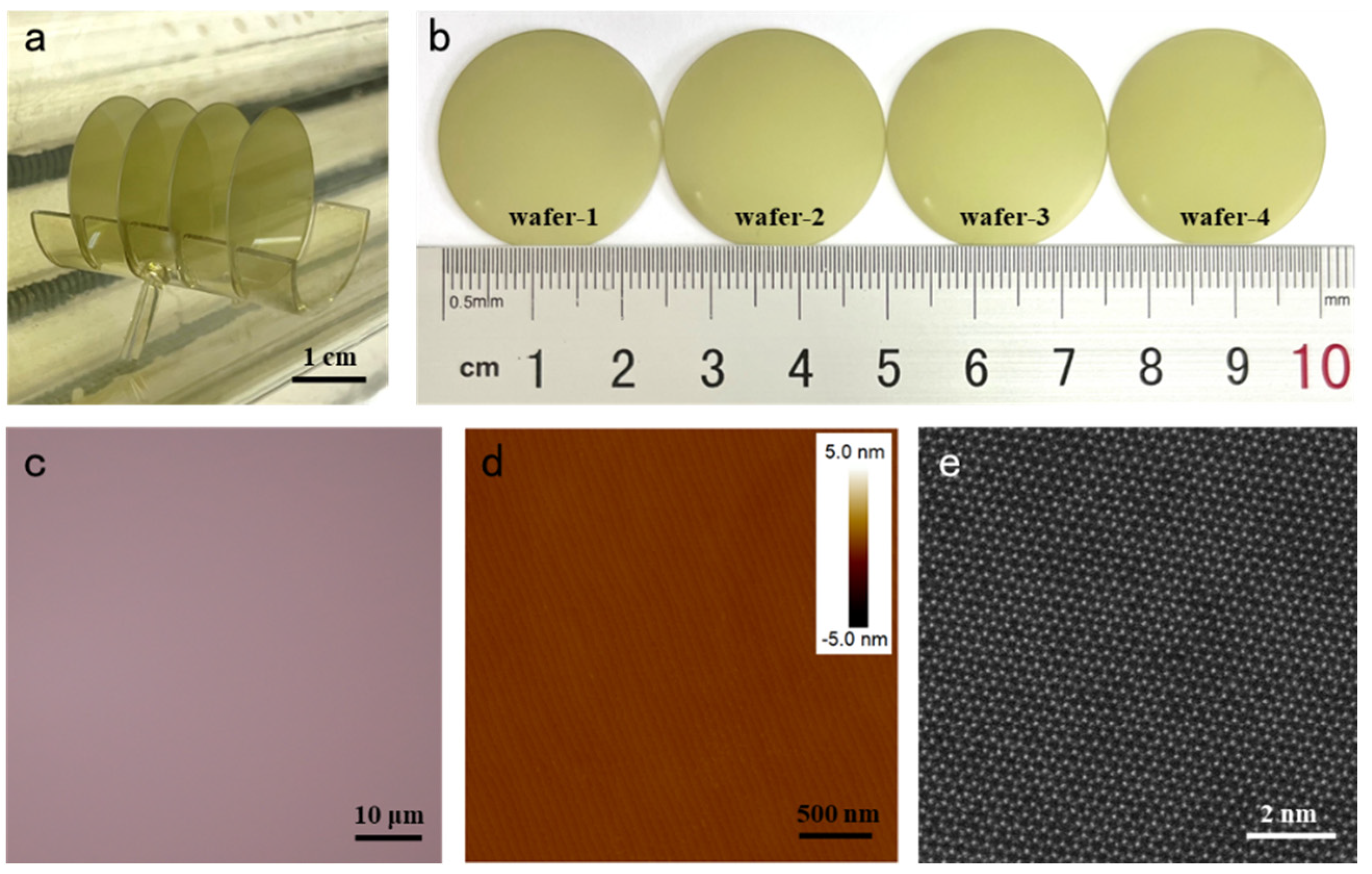
3.1. Morphology Characterization

The batch production of wafer-scale monolayer MoS2 was achieved through CVD. Please refer to Figure S1 for the photograph of the experimental setup. Sulfur powder and molybdenum trioxide powder were used as precursors and were placed in zone I and zone II, respectively. Wafer-scale sapphire substrates were securely held in the grooves of the tailor-made sample holder, and positioned upright in zone III. It is notable that the sapphire substrates were placed along the direction of the carrier gas to guarantee uniform source concentration around each wafer during the growth process. Figure 1a presents one batch of wafer-scale monolayer MoS2 on sapphire substrates, showing four MoS2 wafers within this batch. Actually, the number of MoS2 wafers is limited by the volume of the CVD chamber, and it is worth noting that larger chamber volumes could accommodate more wafers in a single batch production process.
The photograph of the MoS2 wafers grown in the same batch is presented in Figure 1b, showcasing their cleanliness and uniform contrast. Figure 1c demonstrates the optical microscopy image of the monolayer MoS2, which shows a clean surface without any contaminant or multilayer nucleation. Similarly, all other optical microscopy images of the wafers within the batch (refer to Figure S2 for more details) show clean surfaces. The AFM image of the MoS2 monolayer shown in Figure 1d exhibits a flat, smooth and intact surface. Note that the steps on the sample are derived from the underneath sapphire substrate. These substrate steps play a pivotal role in facilitating the nucleation process during the monolayer MoS2 growth. Please also refer to Figure S3 for the AFM image of the bare sapphire substrate. Figure S4 presents the AFM image of the MoS2 ribbon on the sapphire substrate. The measured height at the ribbon’s edge is approximately 0.6 nm, consistent with the thickness of a monolayer MoS2 film. The produced MoS2 monolayers were joined by grains, and we estimated the grain size of the MoS2 monolayer using AFM. Note that we fumigated the sample with steam to discern the grain boundaries. Figure S5 shows the AFM image of the MoS2 sample with clear grain boundaries, and the grain size of the MoS2 sample is about 1 μm. Furthermore, Figure 1e displays the STEM image of the monolayer MoS2. Sulfur atoms and molybdenum atoms are clearly observed and show a typical hexagon structure. The MoS2 sample shows a nearly perfect lattice structure with few defects, indicating the high quality of the batch-produced samples.

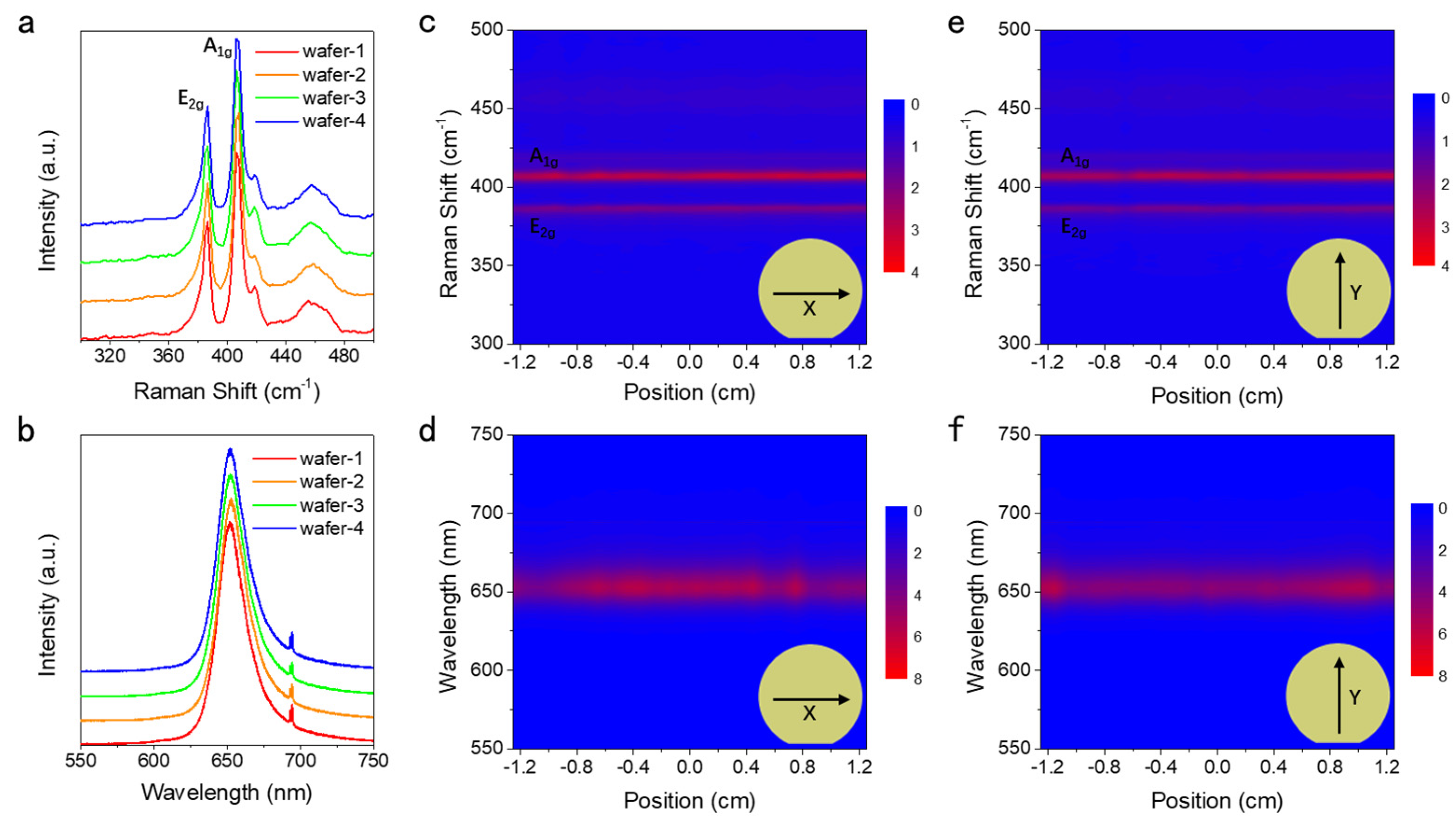
3.2. Optical Spectroscopy and Homogeneity

In order to investigate the homogeneity of the wafer-scale MoS2 samples, optical spectroscopy was performed. Figure 2a presents the Raman spectra of the monolayer MoS2 from the four wafers in one batch. The spectra show characteristic E2g and A1g Raman peaks, corresponding to in-plane and interlayer vibrational modes, respectively [31]. All the spectra exhibit similar peak positions, with the E2g peak and A1g peak located at ~386.2 cm−1 and ~407.1 cm−1, which reveals the high uniformity of different MoS2 wafers in one batch. The average Raman peak separation between the E2g peak and A1g peak was calculated to be 20.9 cm−1. It is crucial to recognize that the separation of Raman peaks can indeed exhibit variations when dealing with grown monolayer MoS2 on different substrates. For example, the peak distance of the monolayer MoS2 grown on sapphire is larger than that grown on SiO2 [32]. Thus, the separation of the Raman peaks for E2g and A1g in this work reflects the monolayer nature of the MoS2 samples. Moreover, the additional peak at ~415 cm−1 corresponds to the sapphire substrates, while the peak at ~450 cm−1 comes from the LA phonon mode at the Brillouin zone boundary (M point) or corner (K point) of MoS2. The PL spectra of the four wafers in one batch are shown in Figure 2b. All the spectra exhibit an obvious photoluminescence peak with a strong intensity, which is rooted in the direct bandgap for monolayer MoS2 [33]. It is notable that the PL peaks for different wafers show a similar position, which indicates the high homogeneity of MoS2 wafers in one batch again.
To further confirm the homogeneity of the wafer-scale monolayer MoS2 film, optical spectroscopy mapping was conducted. The size of a 1-inch MoS2 wafer is approximately 2.5 cm, and we collected 26 points on the wafer for the mapping images along the X- and Y-direction, respectively. Therefore, the spatial resolution of the mapping is 1 mm per point. Figure 2c,d displays the Raman and PL mapping images of the monolayer MoS2 wafer along the X-direction. In the Raman mapping image, the E2g peak and A1g peak are clearly observed and their positions align with those in the Raman spectra shown in Figure 1a. Notably, the peaks in the mapping image show an invariable wavenumber and a consistent intensity along the X-direction for the entire wafer, which confirm the homogeneity of the MoS2 wafer in the X-direction. Similarly, for the PL mapping image along the X-direction, the photoluminescence peaks at ~652.3 nm are distinctly observed and show a constant wavelength and intensity, further proving the homogeneity of the monolayer MoS2 along the X-direction for the whole wafer. As for the Y-direction of the sample, Raman and PL mapping were also performed, and the mapping images are presented in Figure 1e,f. As observed in the mapping images along the X-direction, both the Raman mapping and the PL mapping images along the Y-direction present uniform peak positions and intensity, which indicate the excellent homogeneity of the monolayer MoS2 wafer grown through batch production as well. For additional details, please refer to Figures S6 and S7, which present the normalized raw data of the Raman spectra and PL spectra along both the X- and Y-directions.

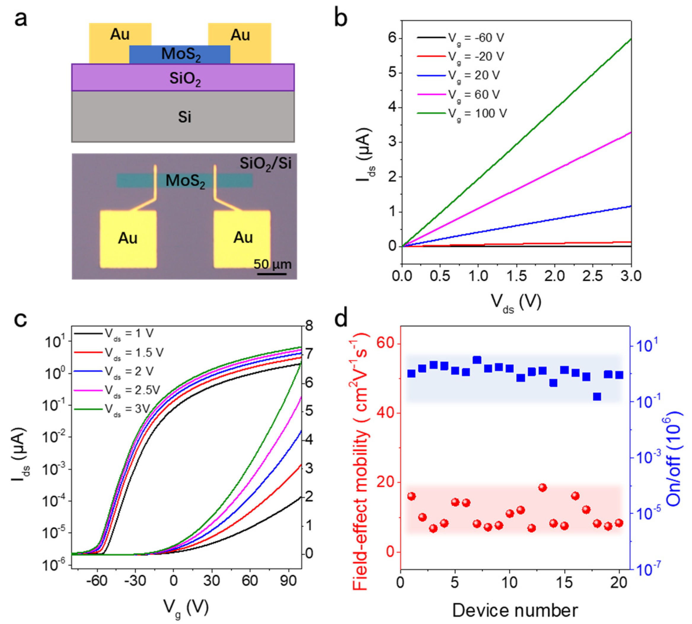
3.3. Electrical Performance of MoS2 Field Effect Transistors (FETs)

For the purpose of characterizing the electrical properties of the monolayer MoS2 synthesized through batch production, back-gate MoS2 FETs on the SiO2/Si substrates were fabricated. The MoS2 monolayers on the SiO2/Si substrates were transferred from the MoS2 monolayers grown on sapphire substrates. The traditional wet transfer method was used for the transfer process to guarantee quality retention. Thus, the texture, crystallinity and quality of the MoS2 monolayers on SiO2/Si substrates were identical to those of the MoS2 monolayers on sapphire substrates. Figure 3a illustrates the schematic diagram of the lateral device structure, along with the photograph of a MoS2 device with a channel length/width of 100/25 μm. The output characteristic curves of the FET are shown in Figure 3b. From the output curves, it is obvious that the source–drain current presents a monotonic increasing trend with the increased bias voltage. Note that the linear nature of the curves indicates excellent ohmic contacts between the as-grown MoS2 monolayer and gold electrodes. Figure 3c shows the transfer characteristic curves of the MoS2 FET, and the curves present typical n-type semiconductor behavior with a high on-state current and low off-state current. Field-effect mobility μ was calculated using the following equation:
μ = [ d I d s / d V g s ] × [ L / ( W C i V d s ) ] ,
where I d s is the source–drain current, V g s is the gate voltage, V d s is the bias voltage, L and W are the channel length and channel width of the device, and C i represents the capacitance of the dielectric layer per unit area [10]. The mobility and on/off ratio of the device is calculated to be 12.25 cm2 V−1 s−1 and 9 × 10⁵.
In order to calculate and acquire the statistical electrical performance of the FETs, we measured 20 devices and analyzed their field-effect mobility and current on/off ratio. The 20 devices were fabricated from the 4 wafers in the same batch, with 5 devices fabricated from each wafer. Statistical data of the field-effect mobility and current on/off ratio of the 20 MoS2 FETs are presented in Figure 3d, and the transfer characteristic curves of these devices are shown in Figure S8. The average mobility of the FETs is calculated to be 10.5 cm2 V−1 s−1 and the on/off ratio averages at 1.3 × 10⁶. In order to compare the performance of the MoS2 FETs with previously reported results, particularly those for the MoS2 samples grown via chemical vapor deposition, we have meticulously compiled a comprehensive summary in Table S1 [19,24,34,35]. The average mobility and the on/off ratio in this work are at a high level compared to the previous results. The results of the electrical performances demonstrate the exceptional quality of the monolayer MoS2 produced via batch production. Moreover, the uniform distribution of the on/off ratio among the 20 devices provides evidence for the homogeneity of the samples. In addition, the mobility variations among different devices are mainly attributed to two key factors. Firstly, discrepancies arise due to the intricacies of the device fabrication process, encompassing aspects such as metal-semiconductor contacts and potential interface contaminations. The second factor contributing to these variations pertains to the presence of grain boundaries and vacancy defects. It is worth noting that the as-grown monolayers are not strict single crystals, and there are a number of grain boundaries in these films. This inherent characteristic leads to mobility variations, as the channels at distinct locations exhibit varying geometries and subsequently differing numbers of grain boundaries and vacancy defects. This intricate interplay results in the observed mobility variations across the devices.

3.4. Batch Production of Oxygen Doped MoS2

Apart from the batch production of MoS2, wafer-scale monolayer oxygen-doped MoS2 can also be produced in batch. Please refer to Figure S9 for a comparison of the MoS2 wafer and MoS2−xOx wafer. The experimental setup and growth parameters of MoS2−xOx wafers are similar to those for MoS2 wafers, while the flow rate of oxygen and the temperature of deposition for MoS2−xOx wafers are different from the parameters for MoS2 wafers. Compared with the growth of MoS2, the flow rate of oxygen is higher and the deposition temperature is lower for the growth of MoS2−xOx [36,37]. Figure 4a presents a photograph of the four monolayer oxygen-doped MoS2 wafers on sapphire substrates grown in a single batch. All the wafers show clean surfaces and uniform contrast, which indicates the successful batch production of MoS2−xOx wafers. An optical microscopy image of the monolayer MoS2−xOx is shown in Figure 4b and the inset of the figure displays an AFM image of the same sample. Both the microscopy image and AFM image demonstrate the absence of distinct contaminants, confirming the excellent cleanliness of batch-produced oxygen-doped MoS2 wafers. The grain size of the oxygen-doped MoS2 was estimated using the optical microscopy image, and we prepared single-crystal samples for the measurement of the grain size. Figure S10 shows the optical microscopy image of the oxygen-doped MoS2 grain, which exhibits a grain size of around 35 μm.
Optical spectroscopy was performed for the oxygen-doped MoS2 monolayers and Figure 4c,d shows the Raman and PL spectra of the monolayer MoS2−xOx obtained from the four wafers in one batch. For the Raman spectra, the peak positions of E2g and A1g show red shifts and blue shifts compared with the peak positions of the intrinsic MoS2 monolayer, respectively. The E2g peak and A1g peak for the monolayer MoS2−xOx are located at ~382 cm−1 and 416 cm−1. It is notable that several new Raman peaks appear for the oxygen-doped MoS2 monolayers, such as the peaks at ~295 cm−1 and 336 cm−1. These new Raman peaks derive from the vibrational modes of Mo-O bonds, which indicate the successful oxygen doping of the MoS2 monolayers. The Raman peaks of the four MoS2−xOx wafers in a single batch show a similar wavenumber and intensity, indicating the uniformity between different wafers. Regarding the PL spectra of the MoS2−xOx wafers, they all show weak photoluminescence peaks, and the peak positions shift to a larger wavelength at ~660 nm compared to intrinsic MoS2. The quench and shift of the PL peaks arise from the transition of the direct bandgap to an indirect bandgap and the reduction in the bandgap due to oxygen doping [37,38]. Note that the PL peaks show a similar shape, wavelength and intensity for the four MoS2−xOx wafers, which proves the homogeneity of the batch-produced samples.

4. Conclusions

In this work, the batch production of monolayer MoS2 wafers was achieved through chemical vapor deposition. The exceptional integrity and cleanliness of the batch-produced samples were confirmed via systematic morphology characterization. Optical spectroscopy measurements further demonstrated the excellent homogeneity of monolayer MoS2 on the wafer scale and the consistency of different wafers within a single batch. The transistors fabricated from batch-produced MoS2 showed outstanding electrical performances, including uniform field-effect mobility and current on/off ratio. Moreover, we extended the batch production method to synthesize monolayer oxygen-doped MoS2 wafers using the same growth process, and the MoS2−xOx wafers presented remarkable cleanliness and uniformity as well, confirming the versatility of our production approach. This work provides a method for improving the production efficiency and reducing the production cost of 2D materials, which will stimulate their development and practical application in diverse fields, especially for large-scale electronic and optoelectronic devices.

Supplementary Materials

The following are available online at https://www.mdpi.com/article/10.3390/cryst13081275/s1, Figure S1. Experimental setup for batch production; Figure S2. Optical microscopy images of MoS2 monolayers in one batch; Figure S3. AFM image of sapphire substrate; Figure S4. AFM image of the MoS2 ribbon on sapphire substrate; Figure S5. Estimate of the crystal grain size of MoS2 by AFM image; Figure S6. Raman spectra of monolayer MoS2; Figure S7. PL spectra of monolayer MoS2; Figure S8. Transfer characteristic curves of MoS2 FETs; Figure S9. Comparison of MoS2 wafer and MoS2−xOx wafer; Figure S10. Estimate of the crystal grain size of MoS2 using optical microscopy image; Table S1. Comparison of performance for MoS2 FET.

Author Contributions

Conceptualization, Z.W. and Y.C.; methodology, Z.W.; formal analysis, Z.W. and Y.C.; investigation, Z.W. and X.S.; data curation, Z.W.; writing—original draft preparation, Z.W.; writing—review and editing, Y.C., Y.L. and Z.Z.; supervision, Y.C.; All authors have read and agreed to the published version of the manuscript.

Funding

This research was funded by National Natural Science Foundation of China, grant number 52171229 and 12204084; Liaoning Province Applied Basic Research Program, grant number 2023JH2/101600045; Liaoning Province Education Department Basic Scientific Research Project, grant number LJKQZ20222301; Dalian Science and Technology Innovation Fund, grant number 2022RQ025.

Data Availability Statement

The data presented in this study are available upon request from the corresponding author.

Conflicts of Interest

The authors declare no conflict of interest.

References

  1. Moore, G.E. Cramming more components onto integrated circuits. Electronics 1965, 38, 114–117. [Google Scholar] [CrossRef]
  2. Kim, S.Y.; Kwak, J.; Ciobanu, C.V.; Kwon, S.Y. Recent developments in controlled vapor-phase growth of 2D group 6 transition metal dichalcogenides. Adv. Mater. 2019, 31, e1804939. [Google Scholar] [CrossRef]
  3. Butler, S.Z.; Hollen, S.M.; Cao, L.; Cui, Y.; Gupta, J.A.; Gutierrez, H.R.; Heinz, T.F.; Hong, S.S.; Huang, J.; Ismach, A.F.; et al. Progress, challenges, and opportunities in two-dimensional materials beyond graphene. ACS Nano 2013, 7, 2898–2926. [Google Scholar] [CrossRef] [PubMed]
  4. Jariwala, D.; Sangwan, V.K.; Lauhon, L.J.; Marks, T.J.; Hersam, M.C. Emerging device applications for semiconducting two-dimensional transition metal dichalcogenides. ACS Nano 2014, 8, 1102–1120. [Google Scholar] [CrossRef]
  5. Li, X.M.; Tao, L.; Chen, Z.F.; Fang, H.; Li, X.S.; Wang, X.R.; Xu, J.B.; Zhu, H.W. Graphene and related two-dimensional materials: Structure-property relationships for electronics and optoelectronics. Appl. Phys. Rev. 2017, 4, 021306. [Google Scholar] [CrossRef]
  6. Akinwande, D.; Huyghebaert, C.; Wang, C.H.; Serna, M.I.; Goossens, S.; Li, L.J.; Wong, H.P.; Koppens, F.H.L. Graphene and two-dimensional materials for silicon technology. Nature 2019, 573, 507–518. [Google Scholar] [CrossRef]
  7. Li, N.; Wang, Q.Q.; Shen, C.; Wei, Z.; Yu, H.; Zhao, J.; Lu, X.B.; Wang, G.L.; He, C.L.; Xie, L.; et al. Large-scale flexible and transparent electronics based on monolayer molybdenum disulfide field-effect transistors. Nat. Electron. 2020, 3, 711–717. [Google Scholar] [CrossRef]
  8. Tang, J.; He, C.L.; Tang, J.S.; Yue, K.; Zhang, Q.T.; Liu, Y.Z.; Wang, Q.Q.; Wang, S.P.; Li, N.; Shen, C.; et al. A reliable all-2D materials artificial synapse for high energy-efficient neuromorphic computing. Adv. Funct. Mater. 2021, 31, 2011083. [Google Scholar] [CrossRef]
  9. Wu, W.; Wang, L.; Li, Y.; Zhang, F.; Lin, L.; Niu, S.; Chenet, D.; Zhang, X.; Hao, Y.; Heinz, T.F.; et al. Piezoelectricity of single-atomic-layer MoS2 for energy conversion and piezotronics. Nature 2014, 514, 470–474. [Google Scholar] [CrossRef]
  10. Radisavljevic, B.; Radenovic, A.; Brivio, J.; Giacometti, V.; Kis, A. Single-layer MoS2 transistors. Nat. Nanotechnol. 2011, 6, 147–150. [Google Scholar] [CrossRef]
  11. Lopez-Sanchez, O.; Lembke, D.; Kayci, M.; Radenovic, A.; Kis, A. Ultrasensitive photodetectors based on monolayer MoS2. Nat. Nanotechnol. 2013, 8, 497–501. [Google Scholar] [CrossRef]
  12. Liu, J.; Chen, X.; Wang, Q.; Xiao, M.; Zhong, D.; Sun, W.; Zhang, G.; Zhang, Z. Ultrasensitive monolayer MoS2 field-effect transistor based DNA sensors for screening of down syndrome. Nano Lett. 2019, 19, 1437–1444. [Google Scholar] [CrossRef] [PubMed]
  13. Wang, L.F.; Liu, D.; Jiang, L.; Ma, Y.X.; Yang, G.L.; Qian, Y.J.; Lei, W.W. Advanced 2D-2D heterostructures of transition metal dichalcogenides and nitrogen-rich nitrides for solar water generation. Nano Energy 2022, 98, 107192. [Google Scholar] [CrossRef]
  14. Dumcenco, D.; Ovchinnikov, D.; Marinov, K.; Lazic, P.; Gibertini, M.; Marzari, N.; Sanchez, O.L.; Kung, Y.C.; Krasnozhon, D.; Chen, M.W.; et al. Large-area epitaxial monolayer MoS2. ACS Nano 2015, 9, 4611–4620. [Google Scholar] [CrossRef] [PubMed]
  15. Shi, J.P.; Ma, D.L.; Han, G.F.; Zhang, Y.; Ji, Q.Q.; Gao, T.; Sun, J.Y.; Song, X.J.; Li, C.; Zhang, Y.S.; et al. Controllable growth and transfer of monolayer MoS2 on Au foils and its potential application in hydrogen evolution reaction. ACS Nano 2014, 8, 10196–10204. [Google Scholar] [CrossRef] [PubMed]
  16. Fu, L.; Sun, Y.; Wu, N.; Mendes, R.G.; Chen, L.; Xu, Z.; Zhang, T.; Rummeli, M.H.; Rellinghaus, B.; Pohl, D.; et al. Direct growth of MoS2/h-BN heterostructures via a sulfide-resistant alloy. ACS Nano 2016, 10, 2063–2070. [Google Scholar] [CrossRef]
  17. Shi, Y.; Zhou, W.; Lu, A.Y.; Fang, W.; Lee, Y.H.; Hsu, A.L.; Kim, S.M.; Kim, K.K.; Yang, H.Y.; Li, L.J.; et al. Van der Waals epitaxy of MoS2 layers using graphene as growth templates. Nano Lett. 2012, 12, 2784–2791. [Google Scholar] [CrossRef]
  18. Yu, H.; Yang, Z.; Du, L.; Zhang, J.; Shi, J.; Chen, W.; Chen, P.; Liao, M.; Zhao, J.; Meng, J.; et al. Precisely aligned monolayer MoS2 epitaxially grown on h-BN basal plane. Small 2017, 13, e1603005. [Google Scholar] [CrossRef]
  19. Zhang, J.; Yu, H.; Chen, W.; Tian, X.Z.; Liu, D.H.; Cheng, M.; Xie, G.B.; Yang, W.; Yang, R.; Bai, X.D.; et al. Scalable growth of high-quality polycrystalline MoS2 monolayers on SiO2 with tunable grain sizes. ACS Nano 2014, 8, 6024–6030. [Google Scholar] [CrossRef]
  20. Yu, H.; Liao, M.; Zhao, W.; Liu, G.; Zhou, X.J.; Wei, Z.; Xu, X.; Liu, K.; Hu, Z.; Deng, K.; et al. Wafer-scale growth and transfer of highly-oriented monolayer MoS2 continuous films. ACS Nano 2017, 11, 12001–12007. [Google Scholar] [CrossRef]
  21. Wang, Q.; Li, N.; Tang, J.; Zhu, J.; Zhang, Q.; Jia, Q.; Lu, Y.; Wei, Z.; Yu, H.; Zhao, Y.; et al. Wafer-scale highly oriented monolayer MoS2 with large domain sizes. Nano Lett. 2020, 20, 7193–7199. [Google Scholar] [CrossRef]
  22. Kim, T.; Mun, J.; Park, H.; Joung, D.; Diware, M.; Won, C.; Park, J.; Jeong, S.H.; Kang, S.W. Wafer-scale production of highly uniform two-dimensional MoS2 by metal-organic chemical vapor deposition. Nanotechnology 2017, 28, 18LT01. [Google Scholar] [CrossRef]
  23. Aljarb, A.; Cao, Z.; Tang, H.L.; Huang, J.K.; Li, M.; Hu, W.; Cavallo, L.; Li, L.J. Substrate lattice-guided seed formation controls the orientation of 2D transition-metal dichalcogenides. ACS Nano 2017, 11, 9215–9222. [Google Scholar] [CrossRef]
  24. Yang, P.; Zhang, S.; Pan, S.; Tang, B.; Liang, Y.; Zhao, X.; Zhang, Z.; Shi, J.; Huan, Y.; Shi, Y.; et al. Epitaxial growth of centimeter-scale single-crystal MoS2 monolayer on Au(111). ACS Nano 2020, 14, 5036–5045. [Google Scholar] [CrossRef] [PubMed]
  25. Kim, H.; Ovchinnikov, D.; Deiana, D.; Unuchek, D.; Kis, A. Suppressing nucleation in metal-organic chemical vapor deposition of MoS2 monolayers by alkali metal halides. Nano Lett. 2017, 17, 5056–5063. [Google Scholar] [CrossRef] [PubMed]
  26. Shi, Y.; Yang, P.; Jiang, S.; Zhang, Z.; Huan, Y.; Xie, C.; Hong, M.; Shi, J.; Zhang, Y. Na-assisted fast growth of large single-crystal MoS2 on sapphire. Nanotechnology 2019, 30, 034002. [Google Scholar] [CrossRef] [PubMed]
  27. Chen, W.; Zhao, J.; Zhang, J.; Gu, L.; Yang, Z.; Li, X.; Yu, H.; Zhu, X.; Yang, R.; Shi, D.; et al. Oxygen-assisted chemical vapor deposition growth of large single-crystal and high-quality monolayer MoS2. J. Am. Chem. Soc. 2015, 137, 15632–15635. [Google Scholar] [CrossRef]
  28. Lin, Z.; Zhao, Y.; Zhou, C.; Zhong, R.; Wang, X.; Tsang, Y.H.; Chai, Y. Controllable growth of large-size crystalline MoS2 and resist-free transfer assisted with a Cu thin film. Sci. Rep. 2015, 5, 18596. [Google Scholar] [CrossRef]
  29. Li, H. Microfabrication techniques for producing freestanding multi-dimensional microstructures. Microsyst. Technol. 2015, 22, 223–237. [Google Scholar] [CrossRef]
  30. Li, M.; Li, W.H.; Zhang, J.; Alici, G.; Wen, W. A review of microfabrication techniques and dielectrophoretic microdevices for particle manipulation and separation. J. Phys. D Appl. Phys. 2014, 47, 063001. [Google Scholar] [CrossRef]
  31. Zhang, X.; Han, W.P.; Wu, J.B.; Milana, S.; Lu, Y.; Li, Q.Q.; Ferrari, A.C.; Tan, P.H. Raman spectroscopy of shear and layer breathing modes in multilayer MoS2. Phys. Rev. B 2013, 87, 115413. [Google Scholar] [CrossRef]
  32. Li, H.; Zhu, X.; Tang, Z.K.; Zhang, X.H. Low-temperature photoluminescence emission of monolayer MoS2 on diverse substrates grown by CVD. J. Lumin. 2018, 199, 210–215. [Google Scholar] [CrossRef]
  33. Splendiani, A.; Sun, L.; Zhang, Y.; Li, T.; Kim, J.; Chim, C.Y.; Galli, G.; Wang, F. Emerging photoluminescence in monolayer MoS2. Nano Lett. 2010, 10, 1271–1275. [Google Scholar] [CrossRef]
  34. Liu, L.; Qiu, H.; Wang, J.; Xu, G.; Jiao, L. Atomic MoS2 monolayers synthesized from a metal-organic complex by chemical vapor deposition. Nanoscale 2016, 8, 4486–4490. [Google Scholar] [CrossRef]
  35. Liu, K.K.; Zhang, W.; Lee, Y.H.; Lin, Y.C.; Chang, M.T.; Su, C.Y.; Chang, C.S.; Li, H.; Shi, Y.; Zhang, H.; et al. Growth of large-area and highly crystalline MoS2 thin layers on insulating substrates. Nano Lett. 2012, 12, 1538–1544. [Google Scholar] [CrossRef] [PubMed]
  36. Tang, J.; Wei, Z.; Wang, Q.; Wang, Y.; Han, B.; Li, X.; Huang, B.; Liao, M.; Liu, J.; Li, N.; et al. In situ oxygen doping of monolayer MoS2 for novel electronics. Small 2020, 16, e2004276. [Google Scholar] [CrossRef] [PubMed]
  37. Wei, Z.; Tang, J.; Li, X.; Chi, Z.; Wang, Y.; Wang, Q.; Han, B.; Li, N.; Huang, B.; Li, J.; et al. Wafer-scale oxygen-doped MoS2 monolayer. Small Methods 2021, 5, e2100091. [Google Scholar] [CrossRef]
  38. Kang, N.; Paudel, H.P.; Leuenberger, M.N.; Tetard, L.; Khondaker, S.I. Photoluminescence quenching in single-layer MoS2 via oxygen plasma treatment. J. Phys. Chem. C 2014, 118, 21258–21263. [Google Scholar] [CrossRef]
Figure 1. Morphology characterization of wafer-scale monolayer MoS2 grown through batch production. (a) One batch of monolayer MoS2 wafers. (b) Photograph of MoS2 wafers grown in the same batch. (c) Optical microscopy image of MoS2 monolayer. (d) AFM image of MoS2 monolayer. Inset is the color-scale bar of height. (e) STEM image of MoS2 monolayer.
Crystals 13 01275 g001
Figure 2. Optical spectroscopy and homogeneity characterization of monolayer MoS2 wafer. (a,b) Raman and PL spectra of monolayer MoS2 from the four wafers in one batch. (c,d) Raman and PL mapping images of wafer-scale monolayer MoS2 along X-direction. Insets show X-direction for the wafer. (e,f) Raman and PL mapping images of wafer-scale monolayer MoS2 along Y-direction. Insets show Y-direction for the wafer.
Crystals 13 01275 g002
Figure 3. Electrical properties of monolayer MoS2 synthesized through batch production. (a) Schematic diagram of device structure laterally and photograph of MoS2 device. (b) Output characteristic curves of the MoS2 FET. (c) Transfer characteristic curves of the MoS2 FET. (d) Statistics of field-effect mobility and on/off ratio of MoS2 transistors.
Crystals 13 01275 g003
Figure 4. Batch production of oxygen-doped MoS2. (a) Photograph of MoS2−xOx wafers grown in the same batch. (b) Optical microscopy image of monolayer MoS2−xOx. Inset: AFM image of monolayer MoS2−xOx. (c,d) Raman and PL spectra of monolayer MoS2−xOx from the four wafers in one batch.
Crystals 13 01275 g004
Disclaimer/Publisher’s Note: The statements, opinions and data contained in all publications are solely those of the individual author(s) and contributor(s) and not of MDPI and/or the editor(s). MDPI and/or the editor(s) disclaim responsibility for any injury to people or property resulting from any ideas, methods, instructions or products referred to in the content.

