Article

Electromagnetically Induced Transparency Analog of Asymmetric Perovskite Metamaterial in the THz Spectral Region

1
Department of Physics and Oxide Research Center, Hankuk University of Foreign Studies, Yongin 17035, Republic of Korea
2
Center for Applied Electromagnetic Research, Advanced Institute of Convergence Technology, Seoul National University, Suwon 16229, Republic of Korea
3
Advanced Center for Laser Science and Spectroscopy, Department of Physics, Hampton University, Hampton, VA 23668, USA
*
Author to whom correspondence should be addressed.
Crystals 2023, 13(7), 1090; https://doi.org/10.3390/cryst13071090
Submission received: 15 June 2023 / Revised: 7 July 2023 / Accepted: 10 July 2023 / Published: 12 July 2023
(This article belongs to the Section Crystal Engineering)

Abstract

:
The analogy of electromagnetically induced transparency (EIT) in perovskite metamaterials is characterized by the numerical simulations in finite-difference time-domain (FDTD). The perovskite metamaterials consist of two cut wire resonators (CWRs) and a disk resonator (DR) on a polyimide substrate. The analysis revealed the characteristic dynamics of the electromagnetic field, the near-field couplings of CWRs and DR, and the EIT-like spectral features of perovskite metamaterials as functions of the asymmetry parameter and polarization direction. The strong coupling and destructive interference of bright and bright–dark transitions in perovskite metamaterials displayed EIT-like transparency at 653.5 GHz with a high Q-factor of approximately 1470, a sensitivity of 531 GHz/RIU and a figure of merit of around 780. In addition, perovskite metamaterials exhibited slow light with a group delay of about 106 ps and a group index of approximately 3100. These results may provide an important perspective for understanding the coupling mechanism and applications of perovskite materials in slow-light devices, THz sensors, and tunable switching in THz spectral region.

1. Introduction

Electromagnetic metamaterials (MMs) have emerged as promising tools for manipulating electromagnetic waves in the terahertz (THz) spectral region, as they differ from natural materials [1,2,3,4,5]. The mechanism of these MMs, whose unit cell is smaller than the operating wavelength, is based on the effective medium approach [4]. The THz frequencies, which range from 100 GHz to 10 THz, have been expected to play an essential role in the sixth generation (6G) and beyond [5]. THz technology has a high potential to alleviate the spectrum shortage and break the capacity limitations of the fourth and fifth-generations (4G and 5G) wireless systems [6]. THz metamaterials have been utilized for various applications, such as switching devices [7,8,9], sensors [10,11], and filters [12]. Controlling the electromagnetic properties makes metamaterials useful for a variety of applications, including sensing and detection in the ~650 GHz frequency band [4,13,14]. Particularly, THz communication is a new field, and metamaterial structures can play an essential role in designing compact and efficient terahertz antennas and imaging devices for future communication systems. In addition, perovskite metamaterial-based sensors can be employed for non-destructive imaging and analysis of biological samples. A typical electromagnetically induced transparency (EIT) is a phenomenon caused by quantum destructive interference between two different excitation paths to the excited state in a three-level atomic system [15,16,17]. The presence of a narrow transparent peak in the EIT signal leads to a strong dispersion effect, accompanied by a large group refractive index. The group refractive index is influenced by the coupling strength between the light and the system. Recently, EIT manipulation has attracted considerable interest in slow light devices [18,19], where the velocity of light can be reduced and controlled [20]. Most approaches for obtaining slow light rely on the EIT effect in extreme experimental conditions [11,12] such as ultra-cold atomic gases, and high-intensity optical pumping. A key aspect of the EIT effect comes from the fact that it enhances the transparency window, which is associated with a strong dispersion. This EIT effect has been extended to MM structures, which exhibit EIT-like effects due to their unique electromagnetic properties. The EIT-like characteristics in MMs arise from the near-field coupling between adjacent resonators and the destructive interference between bright and dark modes, or between bright and bright modes. These EIT-like MMs can be observed and manipulated at room temperature on-chip [21,22,23]. This characteristic makes EIT-like metamaterials promising for use in various areas such as quantum memories [24,25], slow lights [26,27], sensing devices [5,20], and optical modulators [28] for THz applications. In addition, in order to improve the performance of MMs, the most effective way is to achieve a sharp transparent window with a high Q-factor. Recently, perovskites have been reported as a promising material for this purpose, as they have demonstrated remarkable properties for photonic sources [29] and THz modulation [30]. In particular, perovskite is currently one of the most popular materials and represents a material with an ABX3 composite structure. Perovskites are a type of semiconductor, that can change the optical and electrical properties by adjusting the energy bandgap [31]. Compared to silicon-based photovoltaic devices, perovskites have excellent charge mobility [32] and higher efficiency [33,34], which makes them perform remarkably well in optoelectronic [35] and photovoltaic devices [36]. Recent studies have reported on perovskite (CsPbBr3) quantum dots-based heterostructure and quantum dots-embedded metamaterial designed to operate as THz wave modulators [37,38]. THz wave modulation devices [39,40,41] are paving the way for research into photoelectric sensing, high-speed coding and decoding, and low-cost, flexible displays [42,43].
In this paper, a perovskite (CsPbBr3) metamaterial with EIT-like characteristics, tunable slow light, and a high-Q factor in the THz spectral region is presented. The perovskite metamaterial consists of two cut wire resonators (CWRs) and a disk resonator (DR) on a polyimide substrate. Electromagnetic metamaterials are well known to consist of artificially designed units with electromagnetic resonant structures that exhibit strong dispersion and subwavelength properties. In the proposed metamaterial structure, the size parameters of the resonators are smaller than the wavelength ( λ = 440   μ m at 0.68 THz) of the incident electromagnetic wave. The analysis using the finite-difference time-domain (FDTD) technique reveals that the EIT-like spectral features of perovskite metamaterials depend on the asymmetry parameter and polarization direction in the THz spectral region. This paper is organized as follows: The structural design and numerical modeling parameters of the perovskite (CsPbBr3) MM structure are included in Section 2. Section 3 includes a coupled harmonic oscillating system, the EIT-like spectral response as a function of frequency and asymmetry parameters, and the applications of slow-light effects and refractive index sensing.

2. Structure Design and Numerical Model

A unit cell of EIT-like metamaterial, which consists of two CWRs and a DR on the polyimide substrate, is schematically shown in Figure 1. Two CWRs play a role in dipole resonators as bright mode and DR as polarization-independent dark mode. The periodic dimension of the unit cell is P = 440   μ m , and the horizontal distance between two CWRs is h = 1160   μ m . The thickness, relative permittivity, and loss tangent of the perovskite (CsPbBr3) [44] are 20   μ m , ε p = 7.3, and 0.015, respectively. The substrate is polyimide with relative permittivity of 3.75 and loss tangent of 0.0004, whose thickness is 10   μ m . The designed MM structure is characterized by a 3D FDTD solver using a commercial CST Microwave Studio 2022. The unit cell boundary conditions are set in the x- and y-directions and the perfect matching layers are employed in the z-direction. In order to ensure the accuracy of simulation moderate hexahedral mesh size is adopted. As shown in Figure 1, the THz wave with the polarization along the y-axis is normally incident on the perovskite metamaterials, i.e., the plane wave is normally incident along the z-direction and the electric field is along the y-direction, corresponding to the magnetic field along the x-direction.

3. Result and Discussion

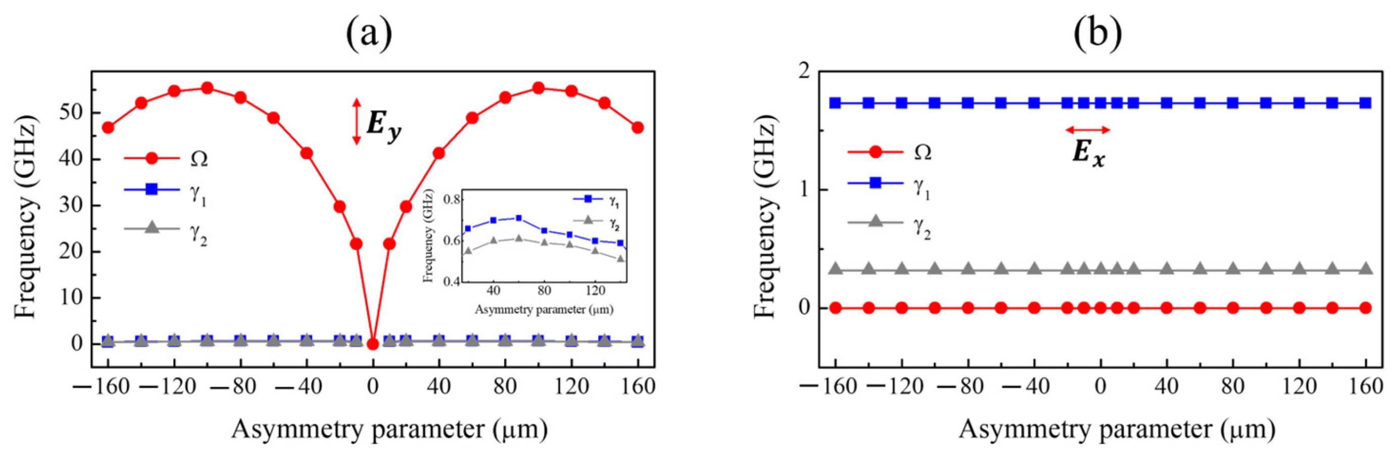
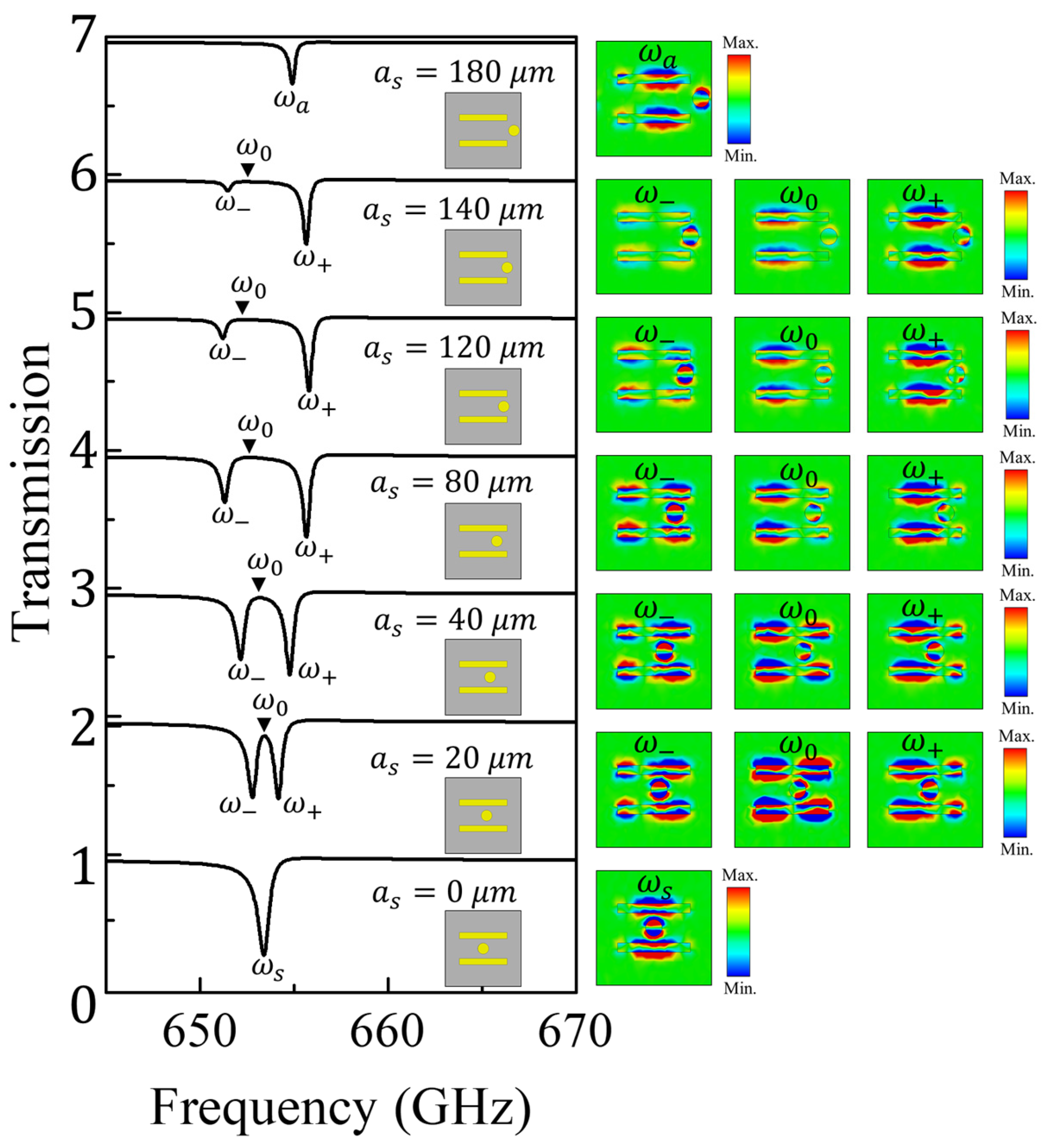
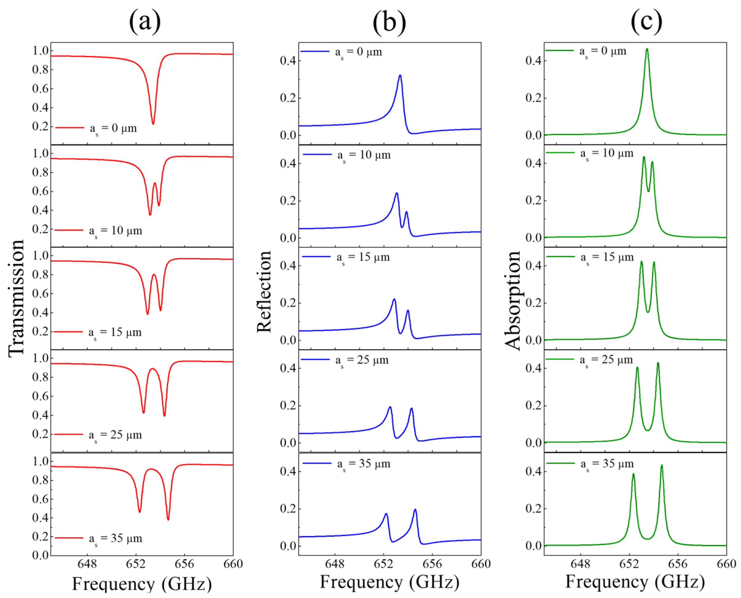
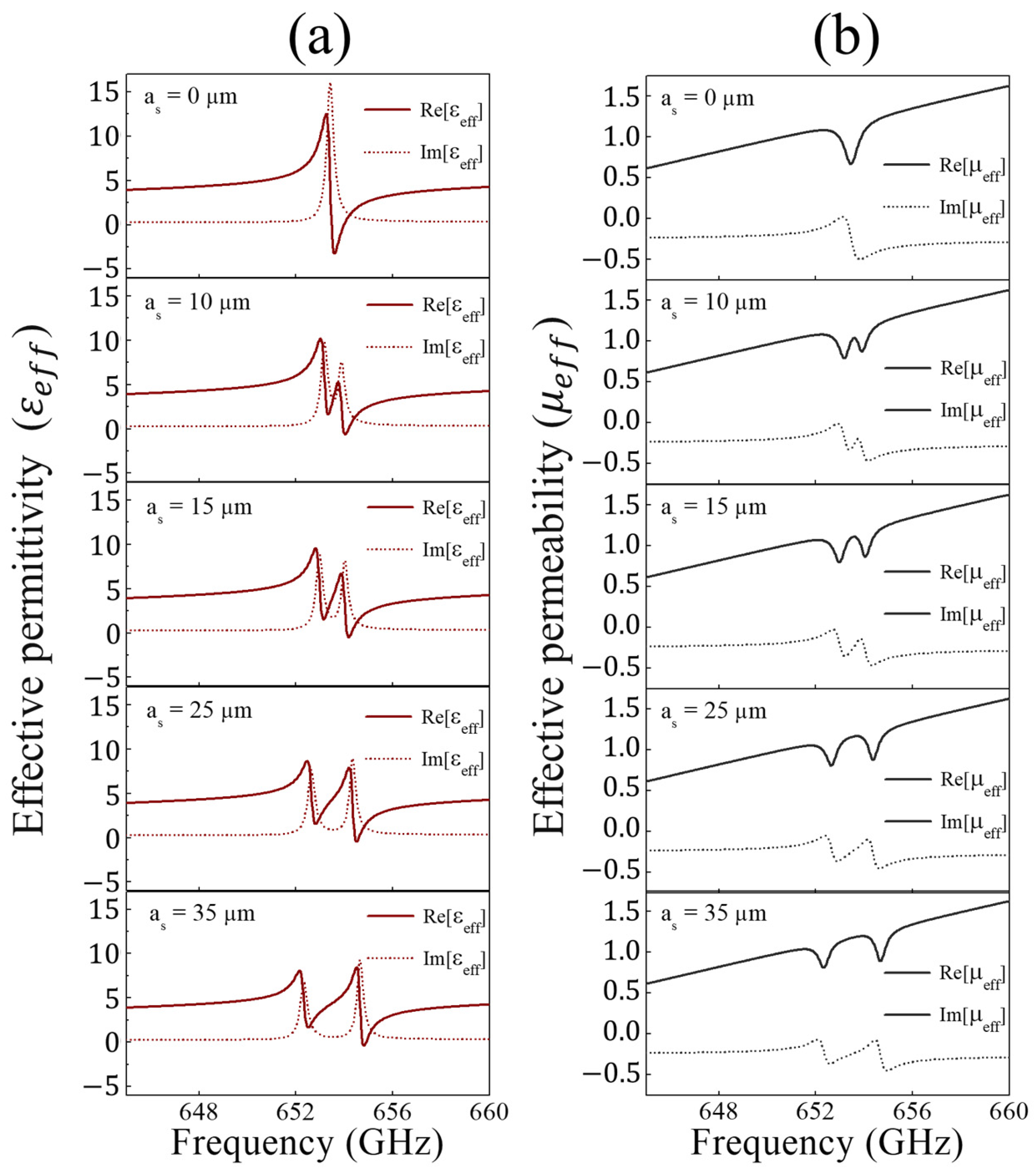
3.1. EIT-like Effect

The three-level system involves a ground state | 0 , a bright mode state | 1 , and a dark mode state | 2 as depicted in Figure 2b,c. The polarization angle θ is defined as the angle of a normally incident wave relative to the y-axis and x-axis, as shown in Figure 2a,b. At first, the normally incident THz wave propagates along the z-direction, and the electric field is aligned with the y-axis ( θ = 0 ° ) . The y-polarized wave can directly and strongly interact with the CWRs, forming the dipole-allowed pathway | 0     | 1 [2,45], as shown in Figure 2c, where the CWRs act as a bright mode. The DR cannot be directly excited by the y-polarized wave, the DR serves as a dark mode resonator, which means the pathway | 0     | 2 is forbidden [2,45]. However, DR can be indirectly excited by CWRs through the near-field coupling between adjacent resonators, allowing for a transition between | 1 and | 2 . When the CWRs and DR are combined into an MM structure with asymmetry parameter a s = 35 μ m , the electromagnetic (EM) energy received in the bright mode is transferred to the dark mode by the effect of near-field coupling, allowing the dark mode to indirectly excite an electric quadrupole resonance, as depicted in Figure 3a. Therefore, there exist two possible pathways to realize the transition from | 0 to | 1 , i.e., | 0     | 1 and | 0     | 1     2   | 1 , both of which lead to strong absorption separately [46,47,48]. The destructive interference between the two possible pathways dramatically suppresses the absorption, which creates the transparency window. The green curve in Figure 3a shows that CWRs, as electric dipole resonators, exhibit a transmission valley at 656 GHz and generate a strong localized electric field at their centers, namely, bright mode. No resonance can be directly observed in DR at 656 GHz as seen from the blue curve in Figure 3a, namely, dark mode. The red curve in Figure 3a demonstrates the transmission spectrum of the MM structure with an asymmetry parameter of 35   μ m . The transparency resonant peak at 653.2 GHz is generated by the near-field coupling between CWRs and DR. As shown in Figure 3a, the MM structure exhibits EIT-like behavior due to the quadrupole-dipole coupling, with CWRs and DR acting as quadrupole and dipole resonators, respectively. For the symmetric case with a s = 0   μ m , the transmission spectrum of the MM structure has no coupling between two modes under the y-polarization as shown by the black curve in Figure 3a. In this case, the MM structure, which is combined with CWRs and DR, acts as a single resonator. For θ = 90 ° , as shown by the green dotted curve in Figure 3b, CWRs act as an electric dipole, with a transmission valley at 655.2 GHz and generate a localized electric field at their ends. However, the DR, shown by the blue dotted curve in Figure 3b, does not have any resonance valley at the same frequency. The black and red dotted curves in Figure 3b ( a s = 0 μ m and a s = 35 μ m ) show the same resonance valley at 653.2 GHz. There is no coupling between CWRs and DR, which means that the destructive interference does not occur under the x-polarized wave.
In the near-field coupling between bright and dark modes, the incident wave excites the bright mode, which transfers electromagnetic energy to the dark mode. This interaction can be described by the linearly coupled Lorentz harmonic oscillator model [49,50,51,52]:
x ¨ 1 t + γ 1 x ˙ 1 t + ω 1 2 x 1 t + Ω 2 x 2 t = g E
x ¨ 2 t + γ 2 x ˙ 2 t + ω 2 2 x 2 t + Ω 2 x 1 t = 0
where x i , ω i , and γ i are the amplitude, resonance frequency, and damping rate of the resonance mode ( i = 1   and   2 for bright and dark modes, respectively). The coupling between the two resonators is defined by the coupling strength Ω and g is a geometric parameter indicating the coupling strength of the bright mode x 1 with the incident electromagnetic field E = E 0 e i ω t . After a certain amount of algebra, the effective susceptibility χ e f f of MM structure can be simplified as follows:
χ e f f = P e f f ε 0 E     = χ r + i χ i = K ω 2 ω 2 2 + i ω γ 2 Ω 4 ω 2 ω 1 2 + i ω γ 1 ω 2 ω 2 2 + i ω γ 2
where K is the proportionality factor K and we assumed that the system has the same resonant frequency ω 0 = ω 1 ,   ω 2   . Here, the real part ( χ r ) and the imaginary part ( χ i ) of the effective susceptibility represent the dispersion and the absorption within the MM structure, respectively. In fitting, the transmission coefficient T is also defined as T = 1 χ i [53]. Transmission coefficient T is given by the Kramer–Kronig relations and it is derived from the conservation of energy relation T + A = 1 , which is normalized to unity. Here A = χ i is the absorption loss within the EIT-like MM structure. Considering the coupling strength effect, the transmission of electromagnetic waves through the MM structure is given as follows [50]:
T = 4 χ e f f + 1 χ e f f + 1 + 1 2 e x p i 2 π d λ 0 χ e f f + 1 χ e f f + 1 1 2 e x p i 2 π d λ 0 χ e f f + 1
where λ 0 is the wavelength in a vacuum, d and χ e f f are the effective thickness and the effective susceptibility of the MM structure, respectively. At the transparency peak where χ r is to zero in Equation (3), the transparency frequency ω T is to the resonant frequency ω 0 . In a lossless model, the effect of the coupling strength Ω on the spectral width of the transparency window can be analyzed by ω + = ω 0 2 + Ω 2 and ω = ω 0 2 Ω 2 . The width of the transparency window is given by [51]
Δ ω = ω + ω = Ω 2 ω 0
Figure 4a displays the EIT-like transmission spectrum with the asymmetry parameter a s = 35 μ m by analytical fitting calculation and simulation results. The analytical fitting result agrees well with the simulated result, with only slight deviations due to the periodicity of the perovskite metamaterial structure [54]. Now, the transmission values for the EIT-like MM structure at ω , ω 0 , and ω + are given as follows: T ( ω ) = 0.459 , T ( ω 0 ) = 0.921 and T ( ω + ) = 0.377 . Here ω = 4.09 × 10 12   rad/s (652.3 GHz), ω 0 = 4.10 × 10 12   rad/s (653.2 GHz) and ω + = 4.11 × 10 12   rad/s (654.6 GHz), respectively. From the above set of Equations (1)–(5), the fitted parameters are obtained as follows: γ 1 = 0.452 × 10 10   rad/s (0.72 GHz), γ 2 = 0.389 × 10 10 rad/s (0.62 GHz), Ω = 2.46 × 10 11 rad/s (39.1 GHz) and K = 3.75 × 10 19 . This result demonstrates the validity of the coupled Lorentz harmonic oscillator model. The fitted parameters γ 1 , γ 2 and Ω , as a function of the asymmetry parameter a s responsible for the coupling strength, are shown in Figure 5. It is interesting that the MM structure has its maximum coupling strength Ω m a x   (55.4 GHz) in the transparency window. The maximum value of a s is defined as a m a x , when the Ω reaches its maximum value Ω m a x . The relationship between the near field coupling strength Ω and asymmetry parameter a s need to be considered under two different cases for y-polarization. When the asymmetry parameter is less than the maximum value ( a s < a m a x ), the coupling strength Ω between two modes increases as the magnitude of the asymmetry parameter   a s increases. However, when the asymmetry parameter is greater than the maximum value ( a s > a m a x ), the coupling strength decreases as the magnitude of asymmetry   a s increases, as shown in Figure 5a. The parameters γ 1 and γ 2 remain almost unchanged with the asymmetry parameter a s , as they are only responsible for the loss associated with the modes. It should be noted that the coupling strength between CWRs and DR becomes stronger for a s < a m a x and then weakens for a s > a m a x , as shown in Figure 5a. Breaking geometrical symmetry induces a transparency window under y-polarized waves. In contrast, there is no coupling between CWRs and DR under x-polarization, as shown in Figure 5b.
Figure 6 displays the transmission spectra and electric field distribution as a function of asymmetry parameters, from a s = 0 μ m to 180   μ m , under the normally incident y-polarized waves. In the near field coupling region, normal mode splitting ( ω ± ) occurs, which is dependent on the coupling strength as shown in Equation (5). The strength of the coupling can be expressed as a function of the asymmetry parameter in Figure 5a and Figure 6. The width of the transparency window widens until the asymmetry parameter reaches about 80   μ m , then narrows after 80   μ m and disappears when a s becomes 180   μ m . When the asymmetry parameter is zero or 180   μ m , there is no coupling effect between CWRs and DR, meaning that the EIT-like effect is not generated when the MM structure is symmetric or when DR is located at the end of the unit cell of the MM structure. As shown in Figure 6, the electric field distribution at the transparent resonance frequency ( ω 0 ) is given by each CWR behaving as a quadrupole and DR as a dipole in the MM structure. When there is no coupling between CWRs and DR, MM structure combined with CWRs and DR exhibits dipole electric field distributions. Hence, as observed in Figure 5a and Figure 6, it can be concluded that the transparency window arises from the destructive interference caused by asymmetric coupling between bright and dark modes under y-polarized waves.
As shown in Figure 7a, the transmission spectra display a transparency peak and two transmitted valleys by changing the asymmetry parameter a s . For a s = 35 μ m , the transmission peak reaches up to 92.1% at 653.2 GHz ( ω 0 ), and two resonant valleys at 652.3 GHz ( ω ) and 654.6 GHz ( ω + ) are observed. The EIT-like peak amplitude increases gradually with the increase of the asymmetry parameter a s , as shown in Figure 7a. The transmission, reflection, and absorption spectra dependence on asymmetry parameter a s are illustrated in Figure 7a–c. When the asymmetry parameter changed from a s = 35   μ m to a s = 0   μ m , the EIT-like peak disappeared and turns into a single transmission valley at 653.2 GHz ( ω s ). The EIT-like effect can be tuned by adjusting the asymmetry parameter a s . The absorption spectra are calculated using a relationship A = 1 T R in Figure 7c, where T and R represent the transmission and reflection, respectively.

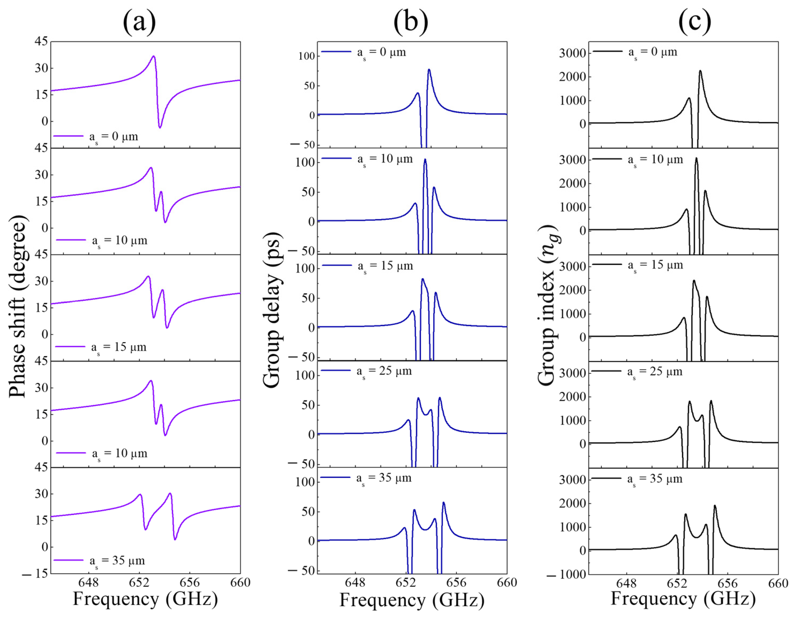
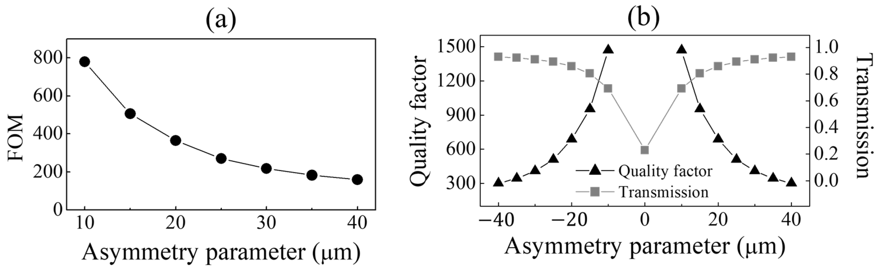
3.2. Slow-Light Effect

The EIT-like effect can slow down the group velocity of THz waves. This slow-light effect is physically related to a large group index that can be produced by extremely steep normal phase dispersion. The transmission phase shift, group delay, and group index in the transparency window are calculated, as depicted in Figure 8a–c. The group velocity is determined by the relationship [55]
v g = d ω d k = c n e f f + ω d n e f f d ω = c n g
where n e f f is the effective refractive index, and k   is the wave vector of THz waves. The group index is defined as n g = n e f f + ω d n e f f d ω . It can be seen that the group slow-light effect can be enhanced by increasing the dispersion of d n e f f d ω . The group index is a crucial parameter for evaluating the slow-light effect, which can be described by [56]
τ g = d ϕ ω d ω ,
n g = c t e f f τ g = c t e f f d ϕ ω d ω
where τ g is the delay time, ϕ ω is the transmission phase shift, c is the velocity of light, t e f f is the effective thickness of the MM structure, and ω is the frequency of the incident wave, respectively. The transmission phase shift is dramatically modified, leading to a change in group delay. As seen in Equations (7) and (8), the values of group delay and group index are proportional to the transmission phase shift relative to the frequency, i.e., d ϕ ω d ω . The phase shift and group delay are modulated at the transparency window, as shown in Figure 8a,b. As the asymmetry parameter a s increases, the dispersion range widens. The group delay and group index as a function of frequency are illustrated in Figure 8b,c. It can be observed that the perovskite MM structure has positive and negative group velocity values. Furthermore, it is worth noting that the steeper the transmission phase shift slope results in a larger group delay. For example, when the asymmetry parameter a s = 10   μ m , the group delay can reach up to about 106 ps at 653.5 GHz. The corresponding group index can reach up to about 3100. As the asymmetry parameter increases gradually, the gradient of phase shift decreases and the slow light effect weakens.
The effective permittivity and the effective permeability of the perovskite MM structure as a function of asymmetry parameter are shown in Figure 9a,b. These results indicate that the designed perovskite MMs can be used for efficient slow-light applications.

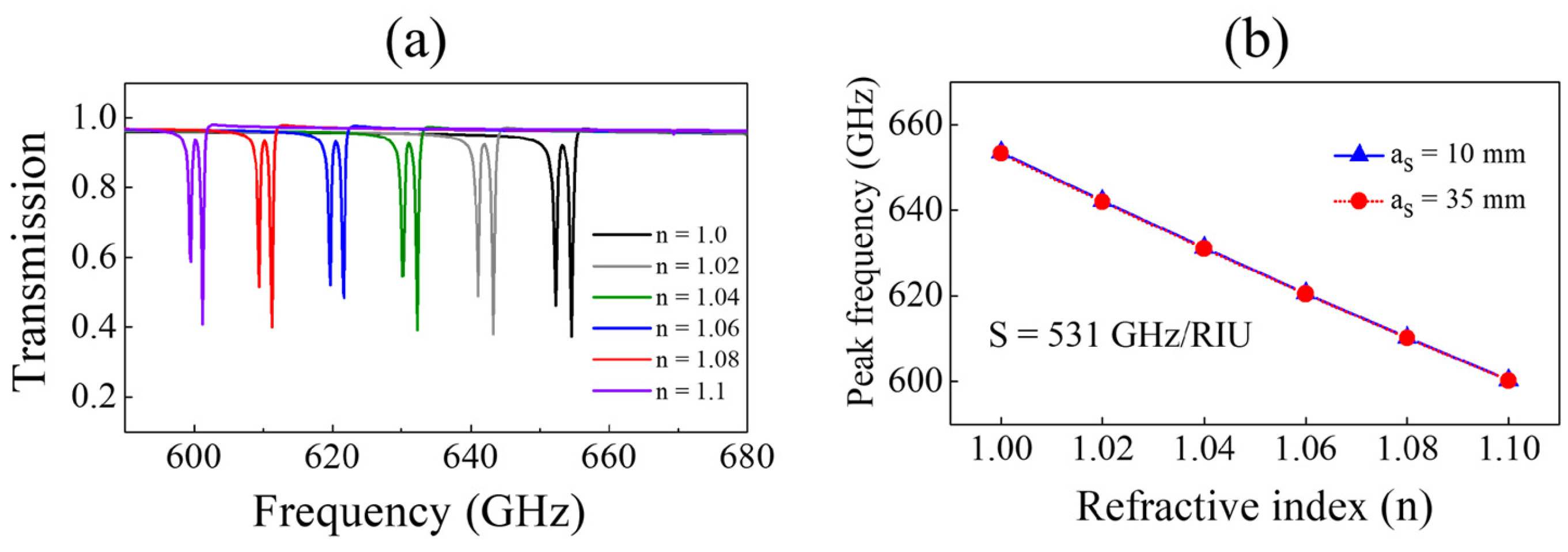
3.3. Refractive-Index Sensing

In general, the sensing of THz MM structure mainly refers to the sensing of the refractive index of the surrounding medium [57,58]. The performance of sensors is usually characterized by sensitivity S, Q-factor, and the figure of merit (FOM). The performance parameter of sensitivity S can be defined as
S = Δ f Δ n
where S is the sensitivity, the unit is GHz/RIU (RIU, Refractive Index Unit), Δ f is the resonant frequency shift, and Δ n is the change of the refractive index, respectively. The figure of merit parameter is obtained by multiplying the sensitivity of the quality factor. The FOM value emphasizes both sensitivity (S) and the quality factor (Q). The FOM value is defined as [59,60]
FOM = S × Q  
where S represents the sensitivity and Q refers to the quality factor of an EIT-like resonant peak. The quality factor (Q-factor) can be obtained by the following formula:
Q = f r FWHM
where the f r is the resonant frequency of maximum transmission at the EIT window, and the FWHM is the full width at half maximum. Equation (10) indicates that a higher Q-factor for a constant S results in a better FOM value, which means better sensor performance. From the above Equations (9)–(11), we discuss the sensing performance of the designed EIT-like sensor for different refractive indices. As shown in Figure 10a,b, when the refractive index increases from 1 to 1.1 by steps of 0.02, the resonant transmission peak of the EIT window shifts 53.1 GHz towards the low-frequency direction ( a s = 0   μ m and 35   μ m ) . For a s = 35   μ m , the transmission peak amplitude of the transparency window reaches 93.5% at n = 1.1 in Figure 10a. Figure 10b shows the EIT peak frequencies change linearly with the refractive index for both a s = 0   μ m and 35   μ m . As the refractive index of the surrounding medium increases, the effective permittivity of the MM structure increases, causing the EIT-like resonance to redshift [8]. It is found that EIT-like resonances for refractive indices from 1 to 1.1 have the same sensing performance, with two slopes of S = 531 GHz/RIU, which represents the refractive index sensitivity of the designed MM structure.
Figure 11a displays that the FOM value increases as the asymmetry parameter a s decreases for y-polarized waves. The Q-factor increases as the magnitude of the asymmetry parameter a s decreases, leading to an increase in the FOM value. A higher Q value indicates the resonant peak is sharper, indicating that the resonator has lower losses and higher energy storage capacity. The Q-factor decreases as the absolute value a s of asymmetry parameter increases, while the transmission peak amplitude gradually increases with the asymmetry parameter a s . In Figure 11a,b, there is one transparency peak in the spectrum with a high Q-factor of about 1470 at a s = 10   μ m , resulting in a corresponding FOM value of about 780. This is because the electric field is mainly concentrated on the EIT-like sensor during EIT-like signal occurrence. It is noted that a slight change in the surrounding medium perturbs the electric field around an EIT-like sensor, causing the EIT-like resonance to shift. Thus, when the electrical and geometrical properties of the material being measured, such as its dielectric constant and thickness, vary, the EIT-like resonance shifts, making it useful for sensing purposes.

4. Conclusions

The numerical simulation in FDTD characterized the bright–dark mode coupling, electromagnetically induced transparency (EIT)-like transparency with a high Q-factor, and slow light propagation in the perovskite metamaterials at the THz spectral region. It was observed that the strong near-field coupling between the two modes was achieved through THz waves when the perovskite MM structure was asymmetric. By adjusting the asymmetry parameter, the EIT-like effect in the perovskite MM structure could be controlled. Unlike previous studies [2,47,48,49,50,51] on the EIT-like effect, it was found that there is a maximum value for the coupling strength between bright–dark modes. This implies that there is a region where the coupling strength increases or decreases with changes to the asymmetry parameter. For an asymmetry a s = 10   μ m , the group index reached up to about 3100 and the corresponding group delay was around 106 ps, indicating a slow-light effect based on perovskite MM as a result of coupling between bright–dark modes. Furthermore, a high Q-factor, high sensitivity, and FOM value was achieved for the EIT-like resonant peak as a refractive index sensor. In particular, the designed asymmetric perovskite MM exhibited a sensitivity of up to 531 GHz/RIU and a FOM value of up to 780 at the resonance frequency 653.5 GHz, with a corresponding Q-factor of about 1470. The numerical simulation results of perovskite metamaterials should pave the way for experimental realizations for applications including slow-light devices, THz sensors, and tunable switching in the THz spectral region.

Author Contributions

Conceptualization, F.J.S. and B.W.L.; methodology, T.-H.K.; formal analysis, T.-H.K.; resources, F.J.S.; writing—original draft preparation, T.-H.K.; writing—review and editing, F.J.S. and B.W.L.; visualization, T.-H.K.; supervision, F.J.S. and B.W.L.; funding acquisition, F.J.S. All authors have read and agreed to the published version of the manuscript.

Funding

This work at Hampton University was supported by NASA NNX15AQ03A and ARO W911NF-15-1-0535.

Data Availability Statement

The data that support the findings of this research are available from the corresponding author upon reasonable request.

Conflicts of Interest

The authors declare no conflict of interest.

References

  1. Yen, T.J.; Padilla, W.J.; Fang, N.; Vier, D.C.; Smith, D.R.; Pendry, J.B.; Basov, D.N.; Zhang, X. Terahertz Magnetic Response from Artificial Materials. Science 2004, 303, 1494–1496. [Google Scholar] [CrossRef] [PubMed] [Green Version]
  2. Liu, N.; Langguth, L.; Weiss, T.; Kastel, J.; Fleichhauer, M.; Pfau, T.; Giessen, H. Plasmonic analogue of electromagnetically induced transparency at the Drude damping limit. Nat. Mater. 2009, 8, 758–762. [Google Scholar] [CrossRef] [PubMed]
  3. Ju, L.; Geng, B.; Horng, J.; Girit, C.; Martin, M.; Hao, Z.; Bechtel, H.A.; Liang, X.; Zettl, A.; Shen, Y.R.; et al. Graphene plasmonics for tunable terahertz metamaterials. Nat. Naontechnol. 2011, 6, 630–634. [Google Scholar] [CrossRef] [PubMed]
  4. Koschny, T.; Kafesaki, M.; Economou, E.N.; Soukoulis, C.M. Effective medium theory of left-handed materials. Phys. Rev. Lett. 2009, 8, 107402. [Google Scholar] [CrossRef] [Green Version]
  5. Xu, C.; Ren, Z.; Wei, J.; Lee, C. Reconfigurable terahertz metamaterials: From fundamental principles to advanced 6G applications. iScience 2022, 25, 103799. [Google Scholar] [CrossRef]
  6. Tonouchi, M. Cutting-edge terahertz technology. Nat. Photonics 2007, 1, 97–105. [Google Scholar] [CrossRef]
  7. Lee, S.H.; Choi, M.; Kim, T.T.; Lee, S.; Liu, M.; Yin, X.; Choi, H.K.; Lee, S.S.; Choi, C.G.; Choi, S.Y.; et al. Switching terahertz waves with gate-controlled active graphene metamaterials. Nat. Mater. 2012, 11, 936–941. [Google Scholar] [CrossRef] [Green Version]
  8. Vendik, I.B.; Vendik, O.G.; Odit, M.A.; Kholodnyak, D.V.; Zubko, S.P.; Sitnikova, M.F.; Turalchuk, P.A.; Zemlyakov, K.N.; Munina, I.V.; Kozlov, D.S.; et al. Tunable Metamaterials for Controlling THz Radiation. IEEE Trans. Terahertz Sci. Technol. 2012, 2, 538–549. [Google Scholar] [CrossRef]
  9. Hu, X.; Zheng, D.; Lin, Y.-S. Actively tunable terahertz metamaterial with single-band and dual-band switching characteristic. Appl. Phys. 2020, 126, 110. [Google Scholar] [CrossRef]
  10. Zhu, L.; Li, H.; Dong, L.; Zhou, W.; Rong, M.; Zhang, X.; Guo, J. Dual-band electromagnetically induced transparency (EIT) terahertz metamaterial sensor. Opt. Mater. Express 2021, 11, 2109–2121. [Google Scholar] [CrossRef]
  11. Hu, H.; Qi, B.; Zhao, Y.; Zhang, X.; Wang, Y.; Huang, X. A graphene-based THz metasurface sensor with air-spaced structure. Front. Phys. 2022, 10, 990126. [Google Scholar] [CrossRef]
  12. Wang, Q.; Gao, B.; Raglione, M.; Wang, H.; Li, B.; Toor, F.; Arnold, M.A.; Ding, H. Design, Fabrication, and Modulation of THz Bandpass Metamaterials. Laser Photonics Rev. 2019, 13, 1900071. [Google Scholar] [CrossRef]
  13. Rappaport, T.S.; Xing, Y.; Kanhere, O.; Ju, S.; Madanayake, A.; Mandal, S.; Alkhateeb, A.; Trichopoulos, G. Wireless Communications and Applications Above 100 GHz: Opportunities and Challenges for 6G and Beyond. IEEE Access 2019, 7, 78729–78757. [Google Scholar] [CrossRef]
  14. Yang, Y.; Shutler, A.; Grischkowsky, D. Measurement of the transmission of the atmosphere from 0.2 to 2 THz. Opt. Express 2011, 19, 8830–8838. [Google Scholar] [CrossRef] [PubMed]
  15. Harris, S.E.; Field, J.E.; Imamoglu, A. Nonlinear Optical Processes Using Electromagnetically Induced Transparency. Phys. Rev. Lett. 1990, 64, 1107–1110. [Google Scholar] [CrossRef]
  16. Boller, K.J.; Imamoglu, A.; Harris, S.E. Observation of Electromagnetically Induced Transparency. Phys. Rev. Lett. 1991, 66, 2593–2596. [Google Scholar] [CrossRef] [Green Version]
  17. Field, J.E.; Hahn, K.H.; Harris, S.E. Observation of Electromagnetically Induced Transparency in Collisionally Broadened Lead Vapor. Phys. Rev. Lett. 1991, 67, 3062–3065. [Google Scholar] [CrossRef]
  18. Gao, E.; Liu, Z.; Li, H.; Xu, H.; Zhang, Z.; Luo, X.; Xiong, C.; Liu, C.; Zhang, B.; Zhou, F. Dynamically tunable dual plasmon-induced transparency and absorption based on a single-layer patterned graphene metamaterial. Opt. Express 2019, 27, 13884–13894. [Google Scholar] [CrossRef]
  19. Totsuka, K.; Kobayashi, N.; Tomita, M. Slow light in coupled resonator-induced transparency. Phys. Rev. Lett. 2007, 98, 213904. [Google Scholar] [CrossRef] [Green Version]
  20. Liu, N.; Weiss, T.; Mesch, M.; Langguth, L.; Eigenthaler, U.; Hirscher, M.; Sonnichsen, C.; Giessen, H. Planar metamaterial analogue of electromagnetically induced transparency for plasmonic sensing. Nano Lett. 2010, 10, 1103–1107. [Google Scholar] [CrossRef]
  21. Zhang, S.; Genov, D.A.; Wang, Y.; Liu, M.; Zhang, X. Plasmonic-induced transparency in metamaterials. Phys. Rev. Lett. 2008, 101, 047401. [Google Scholar] [CrossRef] [Green Version]
  22. Tassin, P.; Zhang, L.; Koschny, T.; Economou, E.N.; Soukoulis, C.M. Low-loss metamaterials based on classical electromagnetically induced transparency. Phys. Rev. Lett. 2009, 102, 053901. [Google Scholar] [CrossRef] [Green Version]
  23. Kurter, C.; Tassin, P.; Zhang, L.; Koschny, T.; Zhuravel, A.P.; Ustinov, A.V.; Anlage, S.M.; Soukoulis, C.M. Classical analogue of electromagnetically induced transparency with a metal-superconductor hybrid metamaterial. Phys. Rev. Lett. 2011, 107, 043901. [Google Scholar] [CrossRef] [Green Version]
  24. Yan, Z.; Wu, L.; Jia, X.; Xie, C.; Peng, K. Quantum entanglement among multiple memories for continuous variables. Adv. Quantum Technol. 2021, 4, 2100071. [Google Scholar] [CrossRef]
  25. Dantan, A.; Bramati, A.; Pinard, M. Atomic quantum memory: Cavity versus single-pass schemes. Phys. Rev. A 2005, 71, 043801. [Google Scholar] [CrossRef] [Green Version]
  26. Safavi-Naeini, A.H.; Mayer Alegre, T.P.; Chan, J.; Eichenfield, M.; Winger, M.; Lin, Q.; Hill, J.T.; Chang, D.E.; Painter, O. Electromagnetically induced transparency and slow light with optomechanics. Nature 2011, 472, 69–73. [Google Scholar] [CrossRef] [Green Version]
  27. Lee, M.; Ruseckas, J.; Lee, C.; Kudriasov, V.; Chang, K.; Cho, H.; Juzeliunas, G.; Yu, I. Experimental demonstration of spinor slow light. Nat. Commun. 2014, 5, 5542. [Google Scholar] [CrossRef] [PubMed] [Green Version]
  28. Fan, Y.; Qiao, T.; Zhang, F.; Fu, Q.; Dong, J.; Kong, B.; Li, H. An electromagnetic modulator based on electrically controllable metamaterial analogue to electromagnetically induced transparency. Sci. Rep. 2017, 7, 40441. [Google Scholar] [CrossRef] [PubMed] [Green Version]
  29. Sutherland, B.R.; Sargent, E.H. Perovskite photonic sources. Nat. Photonics 2016, 10, 295–302. [Google Scholar] [CrossRef]
  30. Innocenti, R.D.; Lin, H.; Navarro-Cía, M. Recent progress in terahertz metamaterial modulators. Nanophotonics 2022, 11, 1485–1514. [Google Scholar]
  31. Ghosh, D.; Welch, E.; Neukirch, A.J.; Zakhidov, A.; Tretiak, S. Polarons in halide perovskites: A perspective. J. Phys. Chem. Lett. 2020, 11, 3271–3286. [Google Scholar] [CrossRef] [PubMed]
  32. Leijtens, T.; Stranks, S.D.; Eperon, G.E.; Lindblad, R.; Johansson, E.M.J.; McPherson, I.J.; Rensmo, H.; Ball, J.M.; Lee, M.M.; Snaith, H.J. Electronic properties of meso-superstructured and planar organometal halide perovskite film: Charge trapping, photodoping, and carrier mobility. ACS Nano 2014, 8, 7147. [Google Scholar] [CrossRef] [PubMed]
  33. Nie, W.; Tsai, H.; Asadpour, R.; Vlancon, J.-C.; Neukirch, A.J.; Gupta, G.; Crochet, J.J.; Chhowalla, M.; Tretiak, S.; Alam, M.A.; et al. High-efficiency solution-processed perovskite solar cells with millimeter-scale grains. Science 2015, 347, 522. [Google Scholar] [CrossRef] [Green Version]
  34. Yang, W.S.; Noh, J.H.; Jeon, N.J.; Kim, Y.C.; Ryu, S.; Seo, J.; Seok, S.I. High-performance photovoltaic perovskite layers fabricated through intramolecular exchange. Science 2015, 348, 1234. [Google Scholar] [CrossRef]
  35. Gu, J.; Singh, R.; Liu, X.; Zhang, X.; Ma, Y.; Zhang, S.; Maier, S.A.; Tian, Z.; Azad, A.K.; Chen, H.T.; et al. Active control of electromagnetically induced transparency analogue in terahertz metamaterials. Nat. Commun. 2012, 3, 1151. [Google Scholar] [CrossRef] [Green Version]
  36. Green, M.A.; Ho-Baillie, A.; Snaith, H.J. The emergence of perovskite solar cells. Nat. Photonics 2014, 8, 506–514. [Google Scholar] [CrossRef]
  37. Shao-He, L.; Jiu-Sheng, L. Terahertz modulator a using CsPbBr3 perovskite quantum dots heterostructure. Appl. Phys. B 2018, 124, 224. [Google Scholar] [CrossRef]
  38. Hong, W.K.; Jiu-Sheng, H.L.; Quan, Y.J. Sensitive terahertz free space modulator using CsPbBr3 perovskite quantum dots-embedded metamaterial. J. Infrared Millim. Terahertz Waves 2020, 41, 557–567. [Google Scholar] [CrossRef]
  39. Zhou, J.; Hu, Y.; Jiang, T.; Ouyang, H.; Li, H.; Sui, Y.; Hao, H.; You, J.; Zheng, X.; Xu, Z.; et al. Ultrasensitive polarization-dependent terahertz modulation in hybrid perovskites plasmon-induced transparency devices. Photonics Res. 2019, 7, 994–1002. [Google Scholar] [CrossRef]
  40. Caputo, M.; Cefarin, N.; Radivo, A.; Demitri, N.; Gigli, L.; Plaisier, J.R.; Panighel, M.; Di Santo, G.; Moretti, S.; Giglia, A.; et al. Electronic structure of MAPbI3 and MAPbCl3: Importance of band alignment. Sci. Rep. 2019, 9, 15159. [Google Scholar] [CrossRef] [Green Version]
  41. Zhang, B.; Lv, L.F.; Shen, J.L. Ultrafast terahertz modulation characteristics of organolead halide perovskite films revealed by time-resolved terahertz spectroscopy. J. Infrared Millim. Waves 2018, 37, 523. [Google Scholar]
  42. Manjappa, M.; Srivastava, Y.K.; Solanki, A.; Kumar, A.; Sum, T.C.; Singh, R. Hybrid lead halide perovskites for ultrasensitive photoactive switching in terahertz metamaterial devices. Adv. Mater. 2017, 29, 1605881. [Google Scholar] [CrossRef]
  43. Cong, C.; Srivastava, Y.K.; Solanki, A.; Sum, T.C.; Singh, R. Perovskite as a platform for active flexible metaphotonic devices. ACS Photonics 2017, 4, 1595–1601. [Google Scholar] [CrossRef]
  44. Shcherbakov-Wu, W.; Sercel, P.C.; Krieg, F.; Kovalenko, M.V.; Tisdale, W.A. Temperature-Independent Dielectric Constant in CsPbBr3 Nanocrystals Revealed by Linear Absorption Spectroscopy. J. Phys. Chem. Lett. 2021, 12, 8088–8095. [Google Scholar] [CrossRef] [PubMed]
  45. Ling, Y.; Huang, L.; Hong, W.; Liu, T.; Luan, J.; Liu, W.; Lai, J.; Li, H. Polarization-controlled dynamically switchable plasmon-induced transparency in plasmonic metamaterial. Nanoscale 2018, 10, 19517–19523. [Google Scholar] [CrossRef] [PubMed]
  46. Fleischhauer, M.; Imamoglu, A.; Marangos, J.P. Electromagnetically induced transparency: Optics in coherent media. Rev. Mod. Phys. 2005, 77, 633. [Google Scholar] [CrossRef] [Green Version]
  47. Vafapour, Z. Slowing down light using terahertz semiconductor metamaterial for dual-band thermally tunable modulator applications. Appl. Opt. 2018, 57, 722–729. [Google Scholar] [CrossRef]
  48. Zhu, L.; Meng, F.; Dong, L.; Wu, Q.; Che, B.-J.; Gao, J.; Fu, J.-H.; Zhang, K.; Yang, G.-H. Magnetic metamaterial analog of electromagnetically induced transparency and absorption. J. Appl. Phys. 2015, 117, 17D146. [Google Scholar] [CrossRef]
  49. Tassin, P.; Zhang, L.; Zhao, R.; Jain, A.; Koschny, T.; Soukooulis, C.M. Electromagnetically induced transparency and absorption in metamaterials: The radiating two-oscillator model and experimental confirmation. Phys. Rev. Lett. 2012, 109, 187401. [Google Scholar] [CrossRef] [Green Version]
  50. Meng, F.Y.; Wu, Q.; Erni, D.; Wu, K.; Lee, J.C. Polarization-independent metamaterial analog of electromagnetically induced transparency for a refractive-index-based sensor. IEEE Trans. Microw. Theory 2012, 60, 3013–3022. [Google Scholar] [CrossRef]
  51. Wang, L.; Guo, X.; Zhang, Y.; Zhou, X.; Yuan, L.; Zhang, P.; Liang, S.; Lan, F.; Zeng, H.; Zhang, T.; et al. Enhanced THz EIT resonance based on the coupled electric field dropping effect within the undulated meta-surface. Nanophotonics 2019, 8, 1071–1078. [Google Scholar] [CrossRef] [Green Version]
  52. Yahiaoui, R.; Burrow, J.A.; Mekonen, S.M.; Sarangan, A.; Mathews, J.; Agha, I.; Searles, T.A. Electromagnetically induced transparency control in terahertz metasurfaces based on bright-bright mode coupling. Phys. Rev. B 2018, 97, 155403. [Google Scholar] [CrossRef] [Green Version]
  53. Cheng, H.; Chen, S.; Yu, P.; Duan, X.; Xie, B.; Tian, J. Dynamically tunable plasmonically induced transparency in periodically patterned graphene nanostrips. Appl. Phys. Lett. 2013, 103, 203112. [Google Scholar] [CrossRef]
  54. Koschny, T.; Markos, P.; Economou, E.N.; Smith, D.R.; Vier, D.C.; Soukoulis, C.M. Impact of inherent periodic structure on effective medium description of left-handed and related metamaterials. Phys. Rev. B 2005, 71, 245105. [Google Scholar] [CrossRef] [Green Version]
  55. Shen, Y.; Wei, B.Z.; Sun, C.R.; Dong, C.B.; Jian, S.S. Graphene spacer-grating-based structure to realize tunable mid-infrared narrow-band plasmonically induced transparency and slow light effect. Appl. Phys. A 2017, 123, 229–238. [Google Scholar]
  56. Zhang, B.; Li, H.; Xu, H.; Zhao, M.; Xiong, C.; Liu, C.; Wu, K. Absorption and slow-light analysis based on tunable plasmon-induced transparency in patterned graphene metamaterial. Opt. Express 2019, 27, 3598–3608. [Google Scholar] [CrossRef]
  57. Karvets, V.G.; Kabashin, A.V.; Barnes, W.L.; Grigorenko, A.N. Plasmonic surface lattice resonances: A review of properties and applications. Chem Rev. 2018, 118, 5912–5951. [Google Scholar] [CrossRef]
  58. Xiao, B.; Wang, Y.; Cai, W.; Xiao, L. Design and prediction of PIT devices through deep learning. Opt. Express 2022, 30, 14985–14997. [Google Scholar] [CrossRef]
  59. Sherry, L.J.; Chang, S.H.; Schatz, G.C.; Van Duyne, R.P.; Wiley, B.J.; Xia, Y.N. Localized surface plasmon resonance spectroscopy of single silver nanocubes. Nano Lett. 2005, 5, 2034–2038. [Google Scholar] [CrossRef]
  60. Cong, L.Q.; Tan, S.Y.; Yahiaoui, R.; Yan, F.P.; Zhang, W.L.; Singh, R. Experimental demonstration of ultrasensitive sensing with terahertz metamaterial absorbers: A comparison with the metasurfaces. Appl. Phys. Lett. 2015, 106, 031107. [Google Scholar] [CrossRef]
Figure 1. Schematic depicting THz transmission through the perovskite metamaterials geometry.
Crystals 13 01090 g001
Figure 2. (a) Schematic of a unit cell. The geometrical parameters are shown as follows: P = 440   μ m ,   L = 280   μ m ,   h = 116   μ m ,   w = 36   μ m ,   r = 32   μ m ,   t = 20   μ m ,   t s = 10   μ m and a s = 0   ~   35   μ m . Coupled and uncoupled three-level systems for the tunable EIT device at (b) the y-polarized wave E y (i.e., polarization angle θ = 0 ° ) and (c) the x-polarized wave E x (i.e., polarization angle θ = 90 ° ). Here Ω and a s represent the coupling strength and the asymmetry parameter, respectively.
Crystals 13 01090 g002
Figure 3. Transmission spectra and electric field distributions of the individual CWRs, the individual DR, and the MM structures ( a s = 0 μ m and a s = 35 μ m ) under the normally incident (a) y-polarized wave E y and (b) x-polarized wave E x . Here a s represents the asymmetry parameter.
Crystals 13 01090 g003
Figure 4. (a) The simulated (solid line) and analytically calculated (dashed-dotted line) transmission spectra of the MM structure ( a s = 35 μ m ) under the normally incident y-polarized wave. The E-field distributions at the resonance frequency of (b) ω and (d) ω + , and the transparent resonance frequency (c) ω 0 .
Crystals 13 01090 g004
Figure 5. Extracted coupling strength Ω and damping parameters γ 1 , γ 2 as a function of the asymmetry parameter a s under the normal incident (a) y-polarized and (b) x-polarized waves.
Crystals 13 01090 g005
Figure 6. Transmission spectra and E-field distributions as a function of frequency for various asymmetry parameters ( a s = 0~ 180   μ m ) under the normally incident y-polarized wave.
Crystals 13 01090 g006
Figure 7. (a) Transmission, (b) reflection, and (c) absorption spectra of perovskite metamaterial structure with different asymmetry parameters ( a s = 0 μ m , 10 μ m , 15 μ m , 25 μ m , and 35 μ m ) under the normally incident y-polarized wave.
Crystals 13 01090 g007
Figure 8. (a) Transmission phase shift, (b) group delay, and (c) group index of perovskite metamaterial structure with different asymmetry parameters ( a s = 0 μ m , 10 μ m , 15 μ m , 25 μ m , and 35 μ m ) under the normally incident y-polarized wave.
Crystals 13 01090 g008
Figure 9. (a) Complex effective permittivity and (b) complex effective permeability of perovskite metamaterial structure with different asymmetry parameters ( a s = 0 μ m , 10 μ m , 15 μ m , 25 μ m , and 35 μ m ) under the normally incident y-polarized wave.
Crystals 13 01090 g009
Figure 10. (a) Refractive-sensitive tunable transmission spectra of the EIT-like P structure for a s = 35   μ m . (b) The EIT-like peak frequency of MM structure as a function of the refractive index of the surrounding medium for two different asymmetric parameters of a s = 10 μ m and 35 μ m .
Crystals 13 01090 g010
Figure 11. (a) Figure of merit (FOM) of perovskite MM structure as a function of asymmetry parameter ( a s = 10~40 μ m ). (b) Q-factor of the transparency window and transmission peak amplitude of perovskite MM structure a function of asymmetry parameters a s changing from 40   μ m to 40   μ m .
Crystals 13 01090 g011
Disclaimer/Publisher’s Note: The statements, opinions and data contained in all publications are solely those of the individual author(s) and contributor(s) and not of MDPI and/or the editor(s). MDPI and/or the editor(s) disclaim responsibility for any injury to people or property resulting from any ideas, methods, instructions or products referred to in the content.

