Abstract
The all-inorganic perovskite CsPbBr3 is a strong candidate for room-temperature, semiconducting radiation detecting applications. With a high stopping power, a large bandgap, and a high mobility-lifetime (μτ) product for both holes and electrons, CsPbBr3 contains all the desirable properties of a room temperature radiation detector. Unfortunately, the production of detector-grade single crystal samples requires high quality starting materials, which must be further processed to achieve the desired purity for semiconducting operation. We have developed a modified zone refining method combining the continuous purification of ternary CsPbBr3 and the subsequent crystal growth step. Taking advantage of this technique, low-cost polycrystalline CsPbBr3 synthesized via solution chemistry processes can be directly used in the production of high-purity, detector-grade crystals. Semi-cylindrical CsPbBr3 single crystal ingots up to 120 mm in length and 22 mm in diameter were obtained. The final product exhibited good chemical stoichiometry and high trace metal purity (2.34 ppm across 73 elements). Detector devices fabricated from the crystal wafers displayed resistivities > 2.0 × 10⁸ Ω·cm and high photocurrent responses. The radiation detectors were able to produce spectroscopy responses to 241Am α-particle. The hole mobility-lifetime (μτH) product of the detectors was determined to be in the range of 1.45 × 10⁻³ cm2/V.
1. Introduction
Room-temperature semiconducting X- and γ-ray detectors are important in homeland security, medical imaging, space applications, and more [1,2,3]. Candidate radiation detection materials must meet specific requirements, such as high mass density and average atomic number leading to a high radiation stopping power and a large bandgap to reduce thermally activated charge carriers [2]. Furthermore, these materials require a high charge carrier mobility-lifetime (μτ) product to achieve a high charge carrier collection efficiency [2,4]. Several compound semiconductor detectors have been developed with these properties, such as HgI2, TlBr, and CdZnTe (CZT). While these materials meet the requirements of radiation detection, each exhibits problems stemming from their chemical and structural properties. For example, HgI2 is too soft for robust device fabrication [5], TlBr experiences ion migration under electrical bias [6], and the benchmark material, CZT, suffers from Te inclusions and high cost of production. As a result, it is important to investigate alternative semiconductor radiation detection materials that can be produced at low cost.
Lead halide perovskites are promising candidates for the development of compound semiconductor detectors due to their optoelectronic properties. Recent reports have demonstrated promising results in photovoltaic applications [7]. Hybrid-organic perovskites such as CH3NH2PbBr3 (MAPbBr3) have been investigated as radiation detectors due to its desirable bandgap and stopping power, along with low leakage currents [7]. Unfortunately, the incongruent melting behaviors and stability issues in the hybrid perovskites prevent their further development as large volume single crystal detectors [8,9].
The all-inorganic perovskites CsPbX3 (X = Cl, Br, I) have been investigated as a promising candidate for radiation detection. These compounds display higher thermal and moisture stabilities in comparison to their hybrid counterparts [10,11]. Amongst these perovskites, single crystal CsPbBr3 has attracted attention for room-temperature semiconducting radiation detection due to its good stability; large band gap (2.25 eV); and high hole mobility-lifetime product (μτH) [12]. Recent reports [11,13] have demonstrated excellent radiation spectroscopy responses from CsPbBr3 single crystal. Furthermore, the defect tolerance of CsPbBr3 is also much higher than CZT [14], allowing it to maintain optimal charge transport properties at a lower purity level [15,16].
Detector quality CsPbBr3 single crystals have been grown using the Bridgman–Stockbarger method by several research groups around the world [11,15,17]. However, the state-of-the-art process [13] employed high purity starting materials, up to USD 10 per gram. These starting materials were subjected to further purification in multiple reaction vessels before crystal growth. This multi-stepped approach with dedicated equipment and separated thermal cycles further drives the cost of crystal production [18]. In this work, we report a series of experimental approaches to purify and grow detector-grade single crystal CsPbBr3 from low-cost, solution synthesized starting materials.
2. Materials and Methods
2.1. Materials and Synthesis
In this work, polycrystalline CsPbBr3 powder was synthesized via chemical co-precipitation. Reagent grade lead (II) oxide (PbO, Sigma-Aldrich, powder < 10 um, ≥99.9%, trace metals basis) and cesium carbonate (Cs2CO3, Alfa Aesar, powder, 99%) were reacted in aqueous hydrobromic acid (HBr, 48% w/w, aq. soln). Solutions of CsBr and PbBr2 in HBr were prepared under continuous stirring. Both solutions were filtered and added together to form CsPbBr3 powder. Methanol (CH3OH, Alfa Aesar, Semiconductor Grade, 99.9% min) was used to wash the powder prior to drying.
The solution synthesis of the polycrystalline CsPbBr3 employed commercially available Cs2CO3 and PbO at a relatively low purity. These materials were chosen as the starting materials to reduce cost of the synthesis and minimize by-product formation. Various starting materials were investigated for their cost per gram (Sigma-Aldrich, St. Louis, MO, USA). Of these materials, Cs2CO3 and PbO were chosen for lower cost and good reactivity. The starting materials Cs2CO3 and PbO were dissolved separately in aqueous HBr with continuous stirring. The solutions were filtered to remove any residual particulate matter. After mixing the two solutions together, CsPbBr3 powder precipitated immediately. Cs2CO3 and PbO react readily with HBr to form the corresponding bromide salts in solution (Equations (1) and (2)):
Cs2CO3 + 2 HBr → 2 CsBr + H2CO3
PbO + 2 HBr → PbBr2 + H2O
The solutions of bromide salts were then combined to form polycrystalline CsPbBr3 powder (Equation (3)).
CsBr + PbBr2 → CsPbBr3
Other starting materials such as lead (II) acetate and lead (II) nitrate were considered for use as a lead source, but ultimately were not chosen due to higher cost per gram or undesirable reaction behaviors (i.e., forming clumps in HBr).
The solution synthesized polycrystalline powder was washed with a copious amount of electronic grade methanol. After washing, some residual HBr still remains in the powder. The excess acid was increased to a pH of 4 by addition of a small amount of Cs2CO3 solution to the suspended CsPbBr3 in methanol. This was tested by litmus paper. Washing and pH correction of the sample removes excess HBr that can corrode metallic components of the drying apparatus and contaminate the sample.
2.2. Purificaton and Crystal Growth
Polycrystalline CsPbBr3 powder was placed inside a 2-inch ID flat-bottom quartz ampoule and dried under vacuum at 120 °C overnight to remove any residual moisture and solvent. The sample was then transferred to two 1-inch ID flat bottom quartz ampoules and heated to 570 °C for 1 h under a slow flow of hydrogen gas. The sample was cooled to room temperature under dynamic flow of H2, then sealed by blowtorch under 0.3 atm of H2.
Once sealed, samples were purified via zone refining. The zone refining equipment employed a narrow-zone high-temperature furnace traveling along a quartz tube (30 mm inner diameter) wrapped in a heavy-duty heating tape (Figure 1a). The tapered quartz tubes containing the samples were placed into the zone refining furnace with the heating tape maintained at a temperature of 130 °C. The narrow-zone furnace was heated to 600 °C and placed in front of the tip of the sample. The furnace was moved from the tip of the sample towards the heel (see Figure 1b), at a speed of 10 mm/h. Once the furnace had fully passed over the sample, the heater was repositioned quickly over the tip of the sample before a new cycle began. Cycles performed at 10 mm/h were repeated 24 times for purification, which was followed by a cycle at 5 mm/h to promote crystal growth. More experimental detail regarding the zone refining setup can be found in our early report [18].
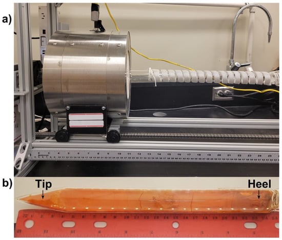
Figure 1.
(a) Zone refining apparatus, with furnace on the left and heating element on the right. (b) An as grown crystal of CsPbBr3 after zone refining.
The fully grown single crystals (shown in Figure 1b) were extracted from the quartz vessel. Semi-cylindrical single crystal grains up to 120 mm long and 22 mm in diameter were obtained consistently. These single crystal samples were then subjected to analyses and detector fabrication.
2.3. Phase Identification via Powder X-ray Diffraction (pXRD)
Phase identification for both the polycrystalline powder and single crystals of CsPbBr3 was conducted via pXRD using a Bruker AXS D2 Phaser with a Cu Kα1 source (λ = 1.54184 Å) from 8 to 80 degrees, with a generator voltage of 10 kV and a generator current of 5 mA. The experimental diffraction patterns were compared to a theoretical pattern. No impurity peak was observed.
2.4. Post-Growth Processing
After growth, the crystal ingots were cut perpendicular to the growth direction into 3.5 mm wafers using a precision saw with a 0.020 mm/s rate. The sliced wafers were bound in epoxy resin. After the epoxy resin was allowed to harden for 48 h, the epoxy-embedded wafers were lapped and polished using a Buehler Precision lapping/polishing machine. Lapping was first performed with successively higher grit SiC sandpapers. Subsequently, fine polishing was achieved using Texpan polishing pads (Pace Technologies, Edmonton, AB, Canada) addressed with deagglomerated (Buehler MicroPolish, Lake Bluff, IL, USA) alumina powder. Polished samples ranged in thickness from 2–3 mm.
2.5. Surface Profilometry Analysis
Surface profilometry analysis was performed prior to contact deposition as a validation of the polishing process. Surface roughness data were taken using a Bruker DektakXT on a polished wafer of CsPbBr3. A single 1 mm line was traced across the surface of each crystal device. The 1 mm line was placed such that it avoided any cracks or visible surface defects.
2.6. Wavelength Energy Dispersive X-ray Spectroscopy (WEDX)
WEDX was used to identify the composition of CsPbBr3 samples. Crystals of CsPbBr3 were embedded in epoxy disks of 2.5 cm diameter. The disks were lapped with a Struers LaboPol-30 using diamond grinding disks (220, 500, 1200 grit) with mineral oil coolant. Polishing was performed using the same instrument with fibre polishing pads, diamond paste (9, 6, 3, 0.25 μm), and mineral oil coolant. Disks were cleaned with methanol. Analysis was performed using a JEOL JXA-8230 electron microprobe with an accelerating potential of 15 kV and a beam current of 10 nA. WEDX confirmed that samples were of a single phase, with a secondary phase at the edge due to oxidation of the sample.
2.7. Photo-Electrical Measurements
Detector devices were fabricated by depositing metallic contacts by electron beam metal evaporation. Indium and gold were deposited in a two-layer deposition on one polished crystal surface, and gold was deposited as a single layer deposition on the other. Colloidal silver paint and copper wire was used to connect the deposited contacts to copper tape pads. Photo-electrical measurements were performed in a grounded dark box. Current density-voltage (J-V) measurements were taken using a Keithley 6517b electrometer with external applied biases ranging between −600 V and 600 V, with each data point being the average of 10 measurements after the prior 5 measurements were removed. Photocurrent measurements were also taken using the same electrometer under applied bias, using a white LED (24 mW) turned on and off at intervals of 10 s.
2.8. Pulse Height Spectrum Measurements
Pulse height measurements were conducted using a Kromek eV-550 preamplifier, an Ortec 428 Detector Bias Supply, an Ortec 575A Amplifier, and an Ortec 928 MCB Analog-to-Digital Converter. The sample setup inside the light-tight sample holder is shown in Figure 2. A pulse height spectrum was obtained from a 241Am source with an activity of 0.9 μCi, using a planar Au/In/CsPbBr3/Au device. Data for each spectrum were collected over 5 m in with a shaping time of 1.5 μs.

Figure 2.
CsPbBr3 crystal device under an 241Am source in an electromagnetic shielded box without the lid.
3. Results and Discussion
3.1. Synthesis and Crystal Growth
Following the solution synthesis, the sample was loaded in a quartz ampoule to be dried at 120 °C for 24 h under a dynamic vacuum. The prolonged drying of the powder under dynamic vacuum is crucial to the formation of high-quality crystals, as the residual solvent can introduce carbon-related impurities [18]. Subsequently, the polycrystalline sample was molten and reduced under a dynamic flow of hydrogen gas. Such a process removes any oxide impurities, which can degrade the electrical properties of the sample and compromise the quartz ampoule. Once fully reduced, the solidified polycrystalline CsPbBr3 was sealed in a new quartz ampoule under 0.3 atm of hydrogen gas. The sealed ampoule containing the sample was then zone refined. As shown in previous work, the hydrogen gas backfill was necessary to supress evaporation of the binary phases. Through this material process protocol, only the final quartz ampoule was flame sealed, while all the other high-purity quartz ampoules/containers were re-etched and re-used to further reduce the cost of production.
The purification of CsPbBr3 was performed by repeated zone refining passes at a speed of 10 mm/h. During these passes, accumulation of darker impurities can be observed accumulating at the heel of the sample (Figure 1b). After the purification passes, the zone refining speed is reduced to 5 mm/h to promote crystal growth. The temperature of the ingot is monitored throughout the passes to ensure that the molten portion of the sample is narrow enough to drive the segregation of impurities. A profile of the temperature per pass is generated to verify the length of the molten zone (~67 mm) in the sample to ensure proper removal of impurities (Figure 3b). As shown in Figure 1a, the zone refining setup employs a heating tape to raise the base temperature of the sample to 130 °C, in order to prevent phase transitions between passes [19]. Following such an experimental protocol, large single crystals were grown with good transparency (Figure 3a).
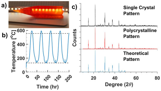
Figure 3.
(a) A crystal ingot from the tip of a zone refined sample. (b) Temperature profile of zone refining. Top line indicates melting point of CsPbBr3 (555 °C), bottom line indicates the temperature of cubic to tetragonal phase transition (130 °C). (c) Powder X-ray diffraction (pXRD) patterns of zone refined (black) and solution synthesized (red)CsPbBr3 comparing to a theoretical pattern (blue).
3.2. Phase Identification of CsPbBr3 via pXRD and Wavelength Dispersive X-ray Spectrometry (WDXS)
The solution synthesized polycrystalline samples and the zone refined single crystals were subjected to phase purity analysis via powder XRD patterns. It was found that CsPbBr3 powder synthesized with a 1:1 molar ratio of Cs2CO3 to PbO resulted in contamination with the lead rich secondary phase. Such an observation is in line with the previous reports on the synthesis of the halide perovskite materials [20]. Increasing the ratio of Cs2CO3 to PbO up to 1.25:1 (molar) resulted in phase pure powders. This is potentially due to the solubility differences of the two binaries in the rinsing solvent used. X-ray diffraction patterns obtained from both the CsPbBr3 powder and single crystal matched the orthorhombic phase well, indicating good phase purities through the protocol (Figure 3c).
Wavelength dispersive X-ray spectrometry (WDXS) technique was employed to confirm the phase purity and verify the stoichiometry of single crystal samples. WDXS analysis verified the mole fraction of elements in a CsPbBr3 single crystal. Mole fractions obtained showed a slight excess of Pb in comparison to Cs (Table 1). The observed lead rich composition is similar to those grown from the high purity materials [18]. Furthermore, Back-scattered electron (BSE) imaging of a sample (Figure 4) indicated the presence of a Cs-rich phase impurity at the edge of the sample. This could be due to moisture degradation of the surface over time prior to WDXS analysis. More work will be conducted to investigate these findings.

Table 1.
Element mole fractions of CsPbBr3 single crystal.
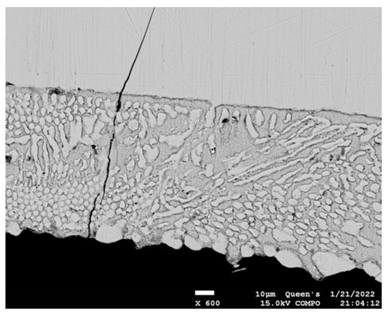
Figure 4.
Back-scattered electron (BSE) image of the edge of a CsPbBr3 crystal.
3.3. Trace Impurity Analysis of CsPbBr3 via Glow Discharge Mass Spectrometry (GDMS)
In order to confirm the effectiveness of the zone refining process, GDMS trace element analysis was performed on single crystal samples extracted from the center of a CsPbBr3 ingot. Elemental analysis revealed that samples purified and grown with this method have extremely high purity considering the quality of the starting materials, with only trace amounts of Na, Mg, Si, S, Cl, Ca, Fe, and Cr (Table 2). Fe and Cr were contaminants from stainless steel tools (i.e., vacuum flanges). Silicon came from the quartz ampoule that the samples were grown in. Calcium and magnesium could be contamination from PbO. Cl is a common contaminant of Br and may be introduced through the use of HBr. Overall, the concentration of impurities totals to less than 3 ppm wt. (μg g−1), thus satisfying the requirement for radiation detection applications. In comparison to samples made from high purity materials, the concentration of heavy metal impurities is similar, while the concentration of Cl is an order of magnitude lower [14]. This is most likely due to the use of HBr as a halide precursor as opposed to Pb and Cs halide salts which could be the source of Cl contamination [14].
Table 2.
Concentrations of trace elements detected by glow discharge mass spectrometry (GDMS).
3.4. Device Fabrication and Photo-Electrical Measurements
Optical flatness is required of single crystal radiation detector devices as a high surface roughness can result in large variations in charge collection behaviors, leading to poorer energy resolutions. To achieve this, CsPbBr3 crystal wafers were cut using a precision saw and embedded in epoxy in order to machine polish the top and bottom surfaces of the crystal without chipping the edges (Figure 5a). Crystal wafers were then polished to a maximum surface roughness of 0.16 μm (Figure 5b). The polished single crystal wafers were fabricated into radiation detectors by depositing metallic contacts in a planar arrangement (i.e., metallization on top and bottom surfaces).
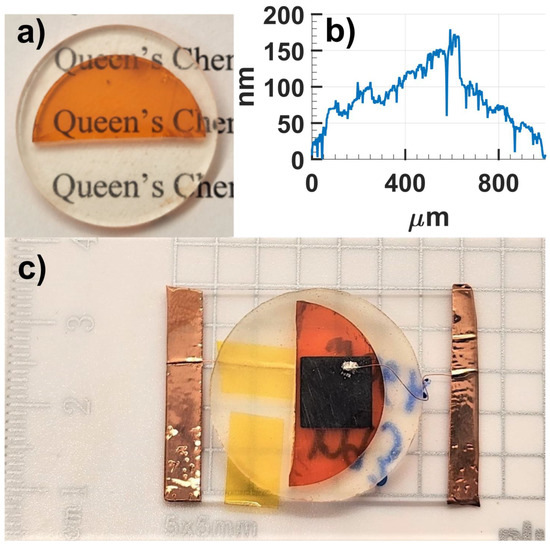
Figure 5.
(a) A polished CsPbBr3 crystal wafer. (b) Profilometry data taken using a Bruker DektakXT on a polished wafer of CsPbBr3. (c) A Au/In/CsPbBr3/Au single crystal device with a 50 nm Au contact on bottom, and a 100 nm In contact on the top surface protected by a 40 nm layer of Au.
Detectors with gold/indium contact on one surface and gold only on the opposite surface (Au/In/CsPbBr3/Au arrangement) showed superior photo responses owing to the blocking nature of the gold/indium–CsPbBr3 interface. The gold layer was deposited over the indium contact to protect it from oxidation. Such an arrangement is similar to the liquid gallium contacts recently reported for CsPbBr3 detectors [21], but more robust. The comparative studies of the electrical contacts will be discussed in a separate report. The final detector devices were prepared by mounting the metalized detectors on glass slides and forming electrical connections between copper wires and the metallic surfaces with colloidal silver paste (Figure 5c).
These devices were characterized via current density-voltage (J-V) tests and photo response measurements. Under an electrical bias from 0 to −600 V, detector devices showed better stability, and higher resistances, in comparison to devices with symmetrical gold contacts (Figure 6a). All samples measured reached a resistivity of >108 Ω·cm in the blocking regime, similar to CsPbBr3 detectors made from the Bridgman–Stockbarger method in other works [9, 14] and meet the requirement of a room temperature radiation detector [4,19]. Photo-response measurements of samples show good signal-to-noise ratios (SNR) of 90, indicating a high photosensitivity (Figure 6b). While the SNR is optimized at −50 and −75 V, the photocurrent experienced instabilities with bias exceeding −100 V. This could be due to surface discharge, or breakdown of the internal electric field. More work is required to understand this instability.
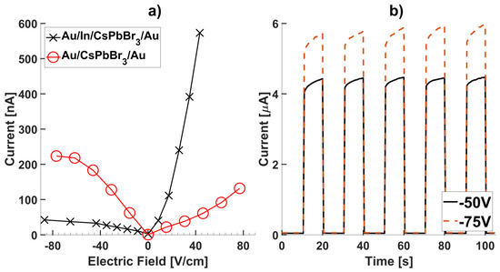
Figure 6.
(a) Current-electric field (J-E) plot of a Au/CsPbBr3/Au device taken from −80 to 80 V/cm (red). Current-electric field (J-E) plot of a Au/In/CsPbBr3/Au device taken from −80 to 80 V/cm (black). (b) Photo-response tests on Au/In/CsPbBr3/Au detector devices.
3.5. Pulse Height Spectrum of CsPbBr3 Devices
The alpha particle response from a 0.9 μCi 241Am source was collected using a detector device prepared from the above-discussed protocol. Energy resolved spectra were obtained across a large range of applied biases (Figure 7a). While the peak counts shifted to higher channel numbers under higher bias, the best energy resolution was obtained at 64 V. At higher voltages, the counts collected by the detector device decreased and the peak broadened. The mobility-lifetime product of holes was evaluated by fitting a Hecht equation over data collected over the entire voltage range, giving a μτH = 3.99 × 10⁻⁵ cm2/V (Figure 7b). This low value is likely related to the large decrease in charge collection efficiency at high voltages. Such behaviors could be caused by an increasing surface conduction at higher voltages, leading to a charge collection dominated by the random discharges. When analyzing the charge collecting data prior to the observed peak broadening, or bias under −40 V (Figure 7a. inset), the Hecht curve fitting results in a μτH = 1.45 × 10⁻³ cm2/V (Figure 7c). In comparison to state-of-the-art CsPbBr3 detectors made from the Bridgman–Stockbarger method, this hole mobility-lifetime value prior to peak broadening is in good accordance [13,14]. This observation revealed the good potential of the zone refined CsPbBr3 single crystals. Improved contact arrangements could significantly improve the performance of these detectors.
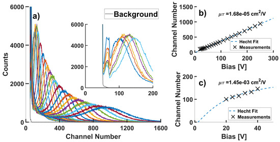
Figure 7.
(a) Pulse height spectrum obtained for a CsPbBr3 detector device with a Au/In/CsPbBr3/Au configuration under biases from 20 V to 250 V, inset shows data collected under applied biases from 20 V to 40 V. (b) Hecht equation fitting for the obtained pulse height spectra. (c) Hecht equation fitting for the obtained pulse height spectra prior to peak broadening, corresponding to (a) inset.
4. Conclusions
Using a modified zone refining process, large detector-grade crystals of CsPbBr3 were purified and grown from low-cost, solution synthesized polycrystalline material. GDMS analysis showed that the single crystals contained a total impurity level of under 3 ppm. Phase purity analyses revealed that no competing phases exist within the grown crystals. Optoelectrical measurements of detector devices made from crystal wafers showed high resistivities, up to 108 Ω·cm, and a good photo response with a SNR of 90 under LED illumination. Pulse height spectra obtained from detector devices showed good charge collection behaviors and were able to resolve alpha particles radiation from a 0.9 μCi 241Am source. These data revealed good potentials of the low-cost CsPbBr3 crystals as semiconducting radiation detectors. Improved radiation detection performances can be achieved through optimization of fabrication protocols and detector contact arrangement.
Author Contributions
Conceptualization, D.A.K., Y.W., R.K. and P.L.W.; methodology, D.A.K.; software, M.F.W.; validation, D.A.K., M.F.W. and P.L.W.; formal analysis, D.A.K. and M.F.W.; investigation, D.A.K.; resources, P.L.W.; data curation, D.A.K. and M.F.W.; writing—original draft preparation, D.A.K.; writing—review and editing, D.A.K., M.F.W., Y.W., R.K. and P.L.W.; visualization, D.A.K. and M.F.W.; supervision, P.L.W.; project administration, P.L.W.; funding acquisition, P.L.W. All authors have read and agreed to the published version of the manuscript.
Funding
This research was funded by the Natural Sciences and Engineering Research Council of Canada (NSERC) and the Canada Foundation for Innovation (CFI). The authors also acknowledge support from the Arthur B. McDonald Canadian Astroparticle Physics Research Institute and the government of Ontario.
Data Availability Statement
Not applicable.
Conflicts of Interest
The authors declare no conflict of interest.
References
- Nakazawa, K.; Takahashi, T.; Watanabe, S.; Sato, G.; Kouda, M.; Okada, Y.; Mitani, T.; Kobayashi, Y.; Kuroda, Y.; Onishi, M.; et al. Large-area CdTe diode detector for space application. Nucl. Instrum. Methods Phys. Res. Sect. A-Accel. Spectrometers Detect. Assoc. Equip. 2003, 512, 412–418. [Google Scholar] [CrossRef]
- Schlesinger, T.E.; Toney, J.E.; Yoon, H.; Lee, E.Y.; Brunett, B.A.; Franks, L.; James, R.B. Cadmium zinc telluride and its use as a nuclear radiation detector material. Mater. Sci. Eng. R-Rep. 2001, 32, 103–189. [Google Scholar] [CrossRef]
- Owens, A. Semiconductor Radiation Detectors; Springer: Boca Raton, Florida, 2019; p. 518. [Google Scholar]
- Kozorezov, A.G.; Wigmore, J.K.; Owens, A.; den Hartog, R.; Peacock, A.; Al-Jawhari, H.A. Resolution degradation of semiconductor detectors due to carrier trapping. Nucl. Instrum. Methods Phys. Res. Sect. A-Accel. Spectrometers Detect. Assoc. Equip. 2005, 546, 209–212. [Google Scholar] [CrossRef]
- Baciak, J.E.; He, Z. Long-term stability of pixelated HgI2 gamma-ray spectrometers operating at room temperature. In Proceedings of the IEEE Nuclear Science Symposium/Medical Imaging Conference, Portland, OR, USA, 19–25 October 2003; pp. 3545–3549. [Google Scholar]
- Hitomi, K.; Kikuchi, Y.; Shoji, T.; Ishii, K. Polarization Phenomena in TlBr Detectors. Ieee Trans. Nucl. Sci. 2009, 56, 1859–1862. [Google Scholar] [CrossRef]
- Stoumpos, C.C.; Kanatzidis, M.G. Halide Perovskites: Poor Man’s High-Performance Semiconductors. Adv. Mater. 2016, 28, 5778–5793. [Google Scholar] [CrossRef] [PubMed]
- Tan, R.; Dryzhakov, B.; Shayotovich, A.; Naylor, A.; Higgins, K.; Charest, J.; Hu, B.; Ahmadi, M.; Lukosi, E.; Ieee. Improved Radiation Sensing with Methylammonium Lead Bromide Perovskite Semiconductors. In Proceedings of the IEEE Nuclear Science Symposium/Medical Imaging Conference (NSS/MIC), Manchester, UK, 26 October–2 November 2019. [Google Scholar]
- Xu, Q.; Wang, X.; Zhang, H.; Shao, W.Y.; Nie, J.; Guo, Y.; Wang, J.; OuYang, X.P. CsPbBr3 Single Crystal X-ray Detector with Schottky Barrier for X-ray Imaging Application. Acs Appl. Electron. Mater. 2020, 2, 879–884. [Google Scholar] [CrossRef]
- Cha, J.H.; Han, J.H.; Yin, W.; Park, C.; Park, Y.; Ahn, T.K.; Cho, J.H.; Jung, D.Y. Photoresponse of CsPbBr3 and Cs4PbBr6 Perovskite Single Crystals. J. Phys. Chem. Lett. 2017, 8, 565–570. [Google Scholar] [CrossRef] [PubMed]
- He, Y.H.; Matei, L.; Jung, H.J.; McCall, K.M.; Chen, M.; Stoumpos, C.C.; Liu, Z.F.; Peters, J.A.; Chung, D.Y.; Wessels, B.W.; et al. High spectral resolution of gamma-rays at room temperature by perovskite CsPbBr3 single crystals. Nat. Commun. 2018, 9, 1609. [Google Scholar] [CrossRef] [PubMed]
- Zhang, X.; Li, F.P.; Bai, R.C.; Sun, Q.H.; Hao, Y.Y.; Xi, S.Z.; Zhu, M.H.; Jiang, S.Q.; Jie, W.Q.; Xu, Y.D. Investigation on energy resolution of CsPbBr3 detectors: From charge transport behavior to device configuration. J. Mater. Chem. C 2022, 10, 6017–6024. [Google Scholar] [CrossRef]
- He, Y.; Petryk, M.; Liu, Z.; Chica, D.G.; Hadar, I.; Leak, C.; Ke, W.; Spanopoulos, I.; Lin, W.; Chung, D.Y.; et al. CsPbBr3 perovskite detectors with 1.4% energy resolution for high-energy γ-rays. Nat. Photonics 2020, 15, 36–42. [Google Scholar] [CrossRef]
- Toufanian, R.; Swain, S.; Becla, P.; Motakef, S.; Datta, A. Cesium lead bromide semiconductor radiation detectors: Crystal growth, detector performance and polarization. J. Mater. Chem. C 2022, 10, 12708–12714. [Google Scholar] [CrossRef]
- Zhang, M.Z.; Zheng, Z.P.; Fu, Q.Y.; Chen, Z.; He, J.L.; Zhang, S.; Chen, C.; Luo, W. Synthesis and single crystal growth of perovskite semiconductor CsPbBr3. J. Cryst. Growth 2018, 484, 37–42. [Google Scholar] [CrossRef]
- Zhang, M.Z.; Zheng, Z.P.; Fu, Q.Y.; Chen, Z.; He, J.L.; Zhang, S.; Yan, L.; Hu, Y.X.; Luo, W. Growth and characterization of all-inorganic lead halide perovskite semiconductor CsPbBr3 single crystals. Crystengcomm 2017, 19, 6797–6803. [Google Scholar] [CrossRef]
- Yu, J.; Liu, G.; Chen, C.; Li, Y.; Xu, M.; Wang, T.; Zhao, G.; Zhang, L. Perovskite CsPbBr3 crystals: Growth and applications. J. Mater. Chem. C 2020, 8, 6326–6341. [Google Scholar] [CrossRef]
- Wu, Y.; Joy, B.; Beyer, S.; Kunar, D.; Kandel, R.; Leybourne, M.; Voinot, A.; Wang, P.L. Combined Purification and Crystal Growth of CsPbBr3 by Modified Zone Refining. Materials Lab. 2022, 1, 20220019. [Google Scholar] [CrossRef]
- Stoumpos, C.C.; Malliakas, C.D.; Peters, J.A.; Liu, Z.F.; Sebastian, M.; Im, J.; Chasapis, T.C.; Wibowo, A.C.; Chung, D.Y.; Freeman, A.J.; et al. Crystal Growth of the Perovskite Semiconductor CsPbBr3: A New Material for High-Energy Radiation Detection. Cryst. Growth Des. 2013, 13, 2722–2727. [Google Scholar] [CrossRef]
- Ramadan, A.J.; Ralaiarisoa, M.; Zu, F.S.; Rochford, L.A.; Wenger, B.; Koch, N.; Snaith, H.J. Revealing the Stoichiometric Tolerance of Lead Trihalide Perovskite Thin Films. Chem. Mater. 2020, 32, 114–120. [Google Scholar] [CrossRef]
- Pan, L.; Feng, Y.X.; Huang, J.S.; Cao, L.R. Comparison of Zr, Bi, Ti, and Ga as Metal Contacts in Inorganic Perovskite CsPbBr3 Gamma-Ray Detector. Ieee Trans. Nucl. Sci. 2020, 67, 2255–2262. [Google Scholar] [CrossRef]


Disclaimer/Publisher’s Note: The statements, opinions and data contained in all publications are solely those of the individual author(s) and contributor(s) and not of MDPI and/or the editor(s). MDPI and/or the editor(s) disclaim responsibility for any injury to people or property resulting from any ideas, methods, instructions or products referred to in the content. |
© 2023 by the authors. Licensee MDPI, Basel, Switzerland. This article is an open access article distributed under the terms and conditions of the Creative Commons Attribution (CC BY) license (https://creativecommons.org/licenses/by/4.0/).