
Study of Nitridation Effect on Structural, Morphological, and Optical Properties of GaAs Film Growth on Silicon Substrates via Close Space Vapor Transport Technique

 , ,
, ,
Abstract
1. Introduction
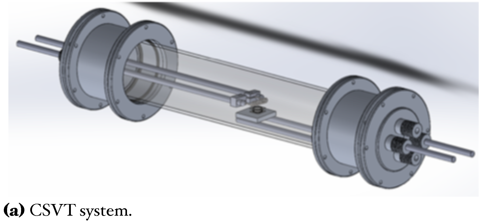
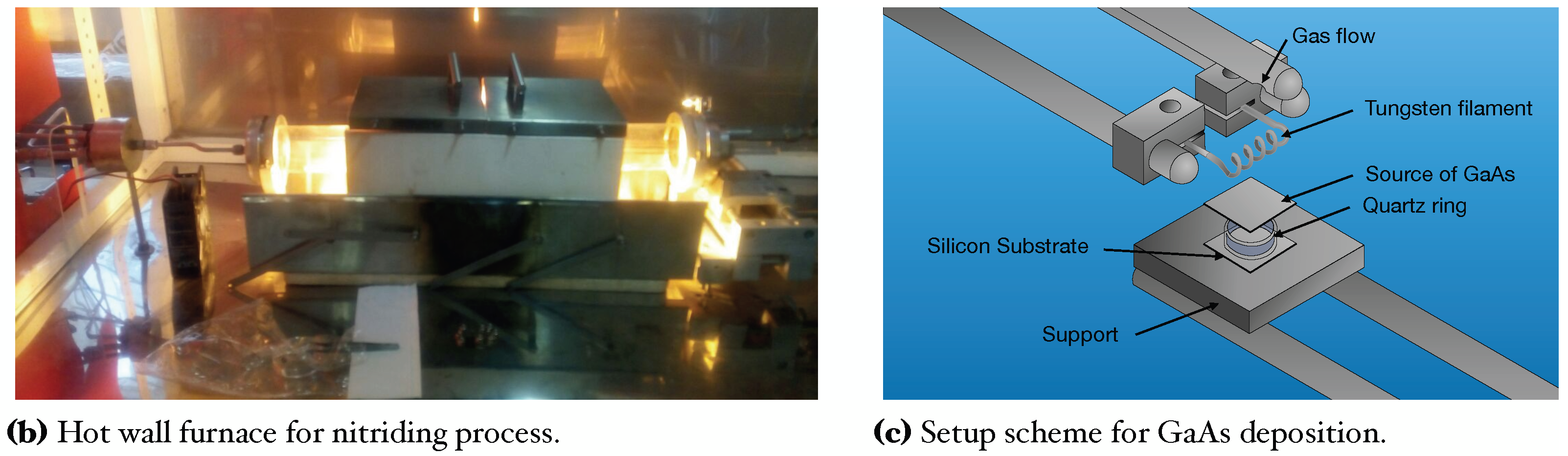
2. Experimental Details
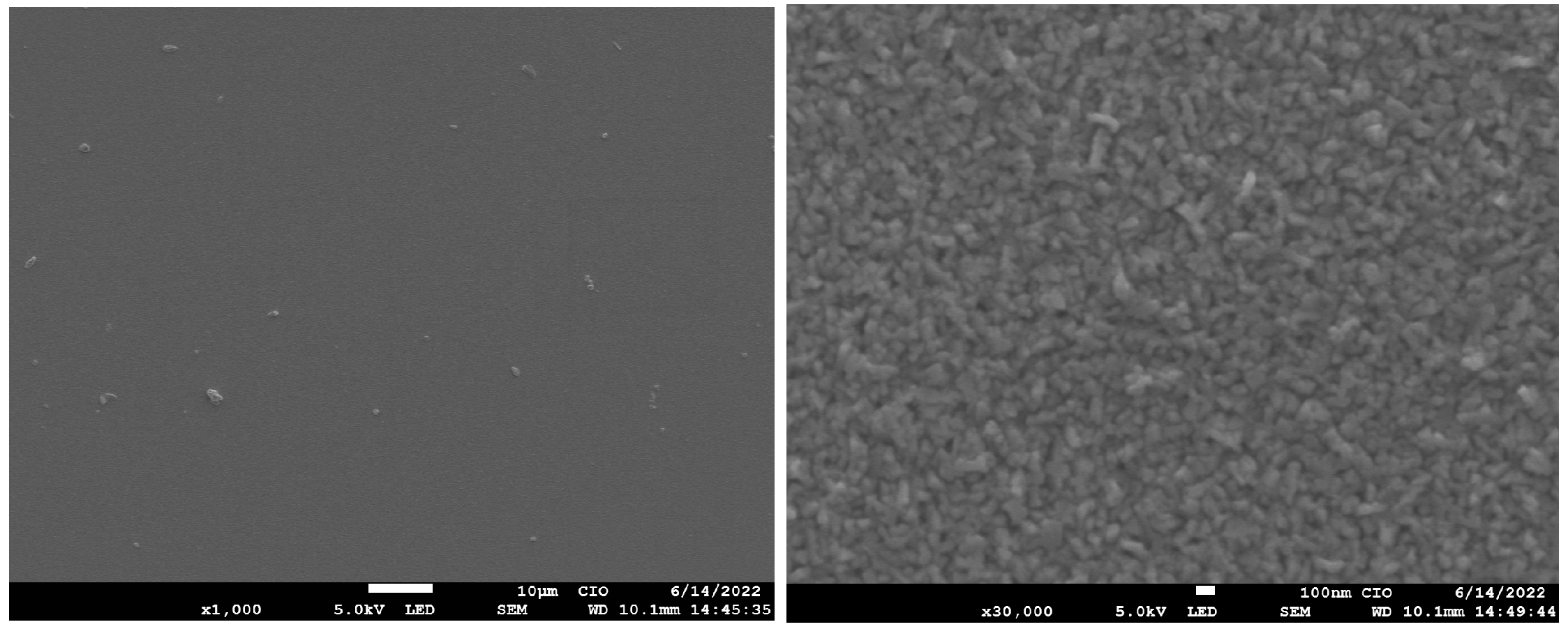
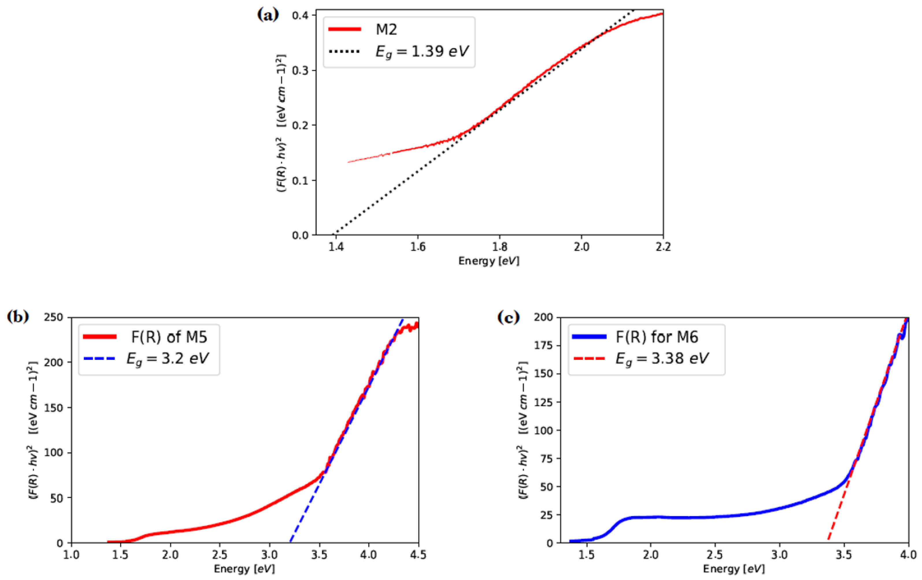
3. Results
4. Conclusions
Author Contributions
Funding
Acknowledgments
Conflicts of Interest
References
- Schlesinger, T. Gallium Arsenide. In Encyclopedia of Materials: Science and Technology; Buschow, K.J., Cahn, R.W., Flemings, M.C., Ilschner, B., Kramer, E.J., Mahajan, S., Veyssière, P., Eds.; Elsevier: Oxford, UK, 2001; pp. 3431–3435. [Google Scholar] [CrossRef]
- Rudolph, P.; Jurisch, M. Bulk growth of GaAs An overview. J. Cryst. Growth 1999, 198, 325–335. [Google Scholar] [CrossRef]
- Yugova, T.G.; Chuprakov, V.A.; Sanzharovsky, N.A.; Yugov, A.A.; Martynov, I.D.; Knyazev, S.N. Effect of a Travelling Magnetic Field on the Parameters of Tellurium-Doped Gallium Arsenide Single Crystals Grown by the Czochralski Method. Crystallogr. Rep. 2022, 67, 1099–1104. [Google Scholar] [CrossRef]
- Heckingbottom, R.; Davies, G.; Prior, K. Growth and doping of gallium arsenide using molecular beam epitaxy (MBE): Thermodynamic and kinetic aspects. Surf. Sci. 1983, 132, 375–389. [Google Scholar] [CrossRef]
- Nishizawa, J.; Kurabayashi, T. Mechanism of gallium arsenide MOCVD. Vacuum 1990, 41, 958–962. [Google Scholar] [CrossRef]
- Szymoński, M.; Bhattacharya, R.S. The sputtering of gallium arsenide at elevated temperatures. Appl. Phys. 1979, 20, 207–211. [Google Scholar] [CrossRef]
- Manasevit, H.M. Single-Crystal Gallium Arsenide on Insulating Substrates. Appl. Phys. Lett. 1968, 12, 156–159. [Google Scholar] [CrossRef]
- Cruz Bueno, J.J.; García Salgado, G.; Balderas Valadez, R.F.; Luna López, J.A.; Nieto Caballero, F.G.; Díaz Becerril, T.; Rosendo Andrés, E.; Coyopol Solís, A.; Romano Trujillo, R.; Morales Ruiz, C.; et al. Effect of the Gaseous Atmosphere in GaAs Films Grown by Close-Spaced Vapor Transport Technique. Crystals 2019, 9, 68. [Google Scholar] [CrossRef]
- Birkmann, B.; Rasp, M.; Stenzenberger, J.; Müller, G. Growth of 3” and 4” gallium arsenide crystals by the vertical gradient freeze (VGF) method. J. Cryst. Growth 2000, 211, 157–162. [Google Scholar] [CrossRef]
- Oshima, R.; Ogura, A.; Shoji, Y.; Makita, K.; Ubukata, A.; Koseki, S.; Imaizumi, M.; Sugaya, T. Ultra-High-Speed Growth of GaAs Solar Cells by Triple-Chamber Hydride Vapor Phase Epitaxy. Crystals 2023, 13, 370. [Google Scholar] [CrossRef]
- Ferhat, M.; Zaoui, A. Structural and electronic properties of III-V bismuth compounds. Phys. Rev. B 2006, 73, 115107. [Google Scholar] [CrossRef]
- Adachi, S. Physical Properties of III-V Semiconductor Compounds; Wiley-VCH: Hoboken, NJ, USA, 1992. [Google Scholar]
- Fujito, K.; Kubo, S.; Nagaoka, H.; Mochizuki, T.; Namita, H.; Nagao, S. Bulk GaN crystals grown by HVPE. J. Cryst. Growth 2009, 311, 3011–3014. [Google Scholar] [CrossRef]
- Humphreys, T.P.; Sukow, C.A.; Nemanich, R.J.; Posthill, J.B.; Rudder, R.A.; Hattangady, S.V.; Markunas, R.J. Microstructural and Optical Characterization of GaN Films Grown by PECVD on (0001) Sapphire Substrates. MRS Online Proc. Libr. (OPL) 1989, 162, 531. [Google Scholar] [CrossRef]
- Papamichail, A.; Kakanakova-Georgieva, A.; Sveinbjörnsson, E.Ö.; Persson, A.R.; Hult, B.; Rorsman, N.; Stanishev, V.; Le, S.P.; Persson, P.O.Å.; Nawaz, M.; et al. Mg-doping and free-hole properties of hot-wall MOCVD GaN. J. Appl. Phys. 2022, 131, 185704. [Google Scholar] [CrossRef]
- Moustakas, T.; Lei, T.; Molnar, R. Growth of GaN by ECR-assisted MBE. Phys. Condens. Matter 1993, 185, 36–49. [Google Scholar] [CrossRef]
- Kucharski, R.; Sochacki, T.; Lucznik, B.; Bockowski, M. Growth of bulk GaN crystals. J. Appl. Phys. 2020, 128, 050902. [Google Scholar] [CrossRef]
- García-Salgado, G.; Cruz-Bueno, J.; Ramírez-González, F.; Gastellou, E.; Nieto-Caballero, F.; Rosendo-Andrés, E.; Luna-López, J.; Coyopol-Solís, A.; Romano-Trujillo, R.; Morales-Ruiz, C.; et al. GaN obtained on quartz substrates through the nitridation of GaAs films deposited via CSVT. J. Alloys Compd. 2021, 887, 161469. [Google Scholar] [CrossRef]
- Richter, T.M.M.; Niewa, R. Chemistry of Ammonothermal Synthesis. Inorganics 2014, 2, 29–78. [Google Scholar] [CrossRef]
- Elke Meissner, R.N. (Ed.) Ammonothermal Synthesis and Crystal Growth of Nitrides; 0933-033X; Springer: Cham, Switzerland, 2021. [Google Scholar]
- Kharisov, B.I.; Oxana, V. Less-Common Methods of the “Direct Synthesis” Area Direct Synthesis of Metal Complexes; Elsevier Science Publishing: Amsterdam, The Netherlands, 2018; pp. 415–433. [Google Scholar]
- Fathy, M.; Gad, S.; Anis, B.; Kashyout, A.E.H.B. Crystal Growth of Cubic and Hexagonal GaN Bulk Alloys and Their Thermal-Vacuum-Evaporated Nano-Thin Films. Micromachines 2021, 12, 1240. [Google Scholar] [CrossRef]
- Runton, D.; Trabert, B.; Shealy, J.; Vetury, R. History of GaN: High-Power RF Gallium Nitride (GaN) from Infancy to Manufacturable Process and Beyond. Microw. Mag. IEEE 2013, 14, 82–93. [Google Scholar] [CrossRef]
- Kobayashi, R.; Fujii, K.F.K.; Hasegawa, F.H.F. Etching of GaAs by Atomic Hydrogen Generated by a Tungsten Filament. Jpn. J. Appl. Phys. 1991, 30, L1447. [Google Scholar] [CrossRef]
- Beloruchev, L.V.; Dembovskii, V.V.; Morshtein, I.M. Method of determining the degree of dissociation of ammonia in different gaseous nitriding processes. Met. Sci. Heat Treat. 1968, 10, 227–228. [Google Scholar] [CrossRef]
- Sukach, G.A.; Kidalov, V.V.; Kotlyarevsky, M.B.; Potapenko, E.P. Structure and composition of gallium nitride films produced by processing gallium arsenide single crystals in atomic nitrogen. Tech. Phys. 2003, 48, 437–440. [Google Scholar] [CrossRef]
- JCPDS—ICDD. Powder Diffraction Files, Swarthmore, PA, Card No. 32-0389, PDF-2 Database (2000). Available online: https://scholar.google.com/scholar_lookup?hl=es-MX&publication_year=2000&pages=%00empty%00&author=JCPDSICDD&isbn=%00null%00&title=Powder+Diffraction+Files#d=gs_cit&t=1680218075343&u=%2Fscholar%3Fq%3Dinfo%3AKZri3gX175wJ%3Ascholar.google.com%2F%26output%3Dcite%26scirp%3D0%26hl%3Des (accessed on 27 February 2023).
- Bernal Correa, R.; Montes Monsalve, J.; Pulzara Mora, A.; López López, M.; Cruz Orea, A.; Cardona, J. Polycristalline growth of zinc blende gallium arsenide layers by R.F. magnetron sputtering. Superf. Vac. 2004, 27, 102–106. [Google Scholar]
- Blakemore, J.S. Semiconducting and other major properties of gallium arsenide. J. Appl. Phys. 1982, 53, R123–R181. [Google Scholar] [CrossRef]
- Coyopol, A.; García-Salgado, G.; Díaz-Becerril, T.; Juárez, H.; Rosendo, E.; López, R.; Pacio, M.; Luna-López, J.A.; Carrillo-López, J. Optical and Structural Properties of Silicon Nanocrystals Embedded in SiOx Matrix Obtained by HWCVD. J. Nanomater. 2012, 2012, 368268. [Google Scholar] [CrossRef]
- Coyopol, A.; Díaz-Becerril, T.; García-Salgado, G.; Juárez-Santisteban, H.; López, R.; Rosendo-Andrés, E. Evolution on the structural and optical properties of SiOx films annealed in nitrogen atmosphere. J. Lumin. 2014, 145, 88–93. [Google Scholar] [CrossRef]
- Saron, K.M.A.; Ibrahim, M.; Hashim, M.R.; Taha, T.A.; Elfadill, N.G.; Mkawi, E.M.; Allam, N.K. Leakage current reduction in n-GaN/p-Si (100) heterojunction solar cells. Appl. Phys. Lett. 2021, 118, 023902. [Google Scholar] [CrossRef]
- Sulikowski, B.; Olejniczak, Z.; Corberán, V.C. Faujasite Catalysts Promoted with Gallium Oxide: A Physicochemical Study. J. Phys. Chem. 1996, 100, 10323–10330. [Google Scholar] [CrossRef]
- Dadgar, A.; Alam, A.; Riemann, T.; Bläsing, J.; Diez, A.; Poschenrieder, M.; Strassburg, M.; Heuken, M.; Christen, J.; Krost, A. Crack-Free InGaN/GaN Light Emitters on Si(111). Phys. Status Solidi (A) 2001, 188, 155–158. [Google Scholar] [CrossRef]
- Chen, Z.; Jaramillo, T. The Use of UV-Visible Spectroscopy to Measure the Band Gap of a Semiconductor; Department of Chemical Engineering, Stanford University: Stanford, CA, USA, 2017. [Google Scholar]


| Sample | Growth Temperature 1st Step | GaAs Deposit Time | Nitriding Temperature 2nd Step | Nitriding Time | Composition Weight % | Thickness | |||
|---|---|---|---|---|---|---|---|---|---|
| C | min | C | min | Ga | As | O | N | nm | |
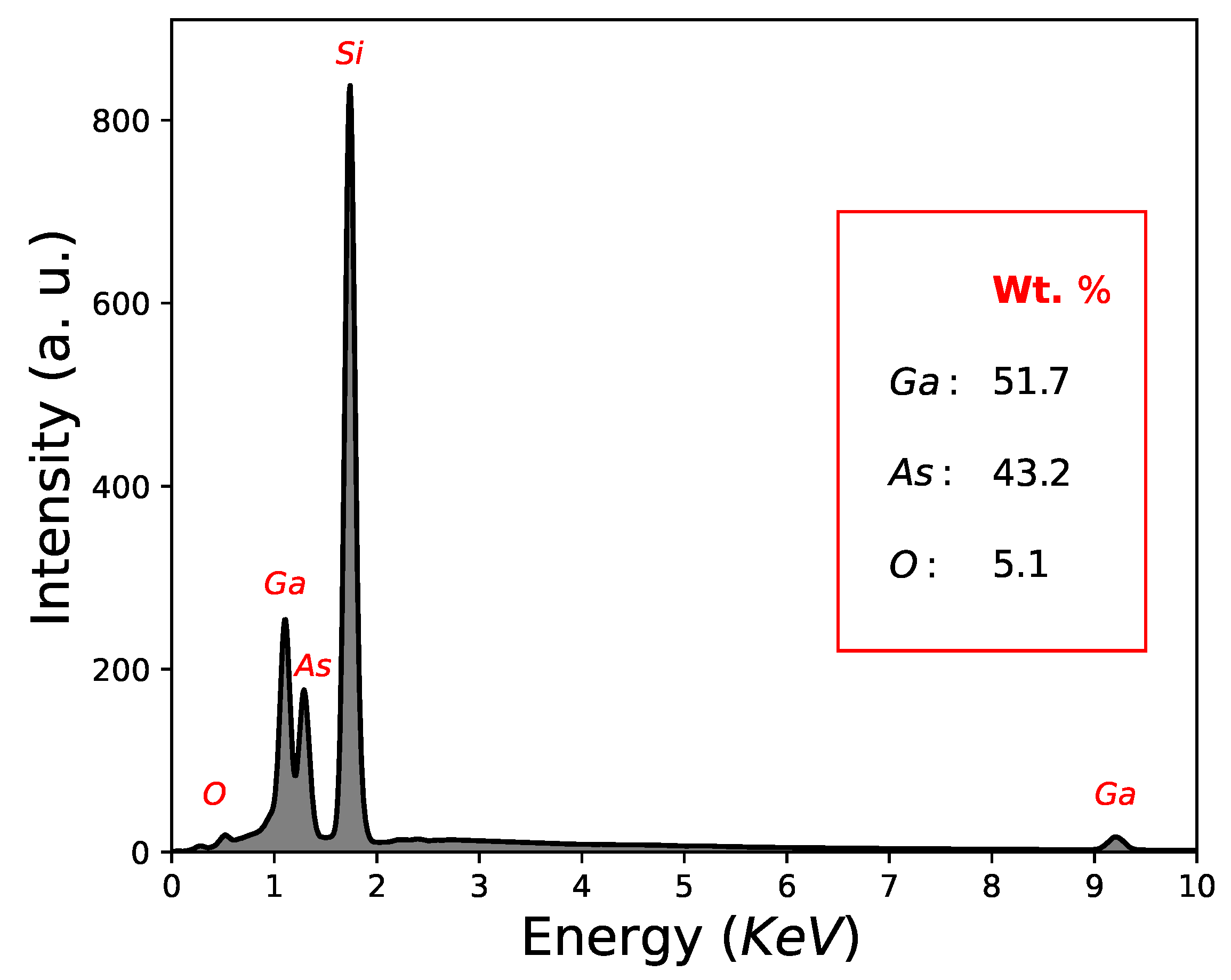
| M2 (GaAs) | 900 | 5 | - | - | 51.7 | 43.2 | 5.1 | - | 641 |
| M4 (GaN) | 800 | 5 | 900 | 30 | 78.5 | 1.9 | 2.1 | 17.5 | 340 |
| M5 (GaN) | 900 | 5 | 900 | 30 | 81.8 | 1.8 | 2.1 | 14.3 | 342 |
| M6 (GaN) | 1000 | 5 | 900 | 30 | 76.8 | 1.7 | 1.9 | 19.6 | 323 |
| SAMPLE | GaAs Results | ||||
|---|---|---|---|---|---|
| Deposit Temperature in Substrate | Position in (111) | FWHM (111) | Crystallite Size [nm] | Lattice Constant [Å] | |
| M1 | 800 C | 27.39 | 0.687 | 12.3 | 5.633 |
| M2 | 900 C | 27.40 | 0.588 | 14.8 | 5.631 |
| M3 | 1000 C | 27.48 | 0.817 | 10.1 | 5.616 |
| SAMPLE | GaAs Results | ||||
|---|---|---|---|---|---|
| Position in (002) | FWHM (002) | Crystallite Size [nm] | Lattice Constant a = b [Å] | Lattice Constant c [Å] | |
| M4 | 34.52º | 0.802º | 9.21 | 3.157 | 5.192 |
| M5 | 34.56º | 0.961º | 7.68 | 3.156 | 5.186 |
| M6 | 34.88º | 0.614º | 12.03 | 3.142 | 5.170 |
| SAMPLE | GaAs | GaN | ||||
|---|---|---|---|---|---|---|
| TO [cm] | LO [cm] | [cm] | [cm] | [cm] | [cm] | |
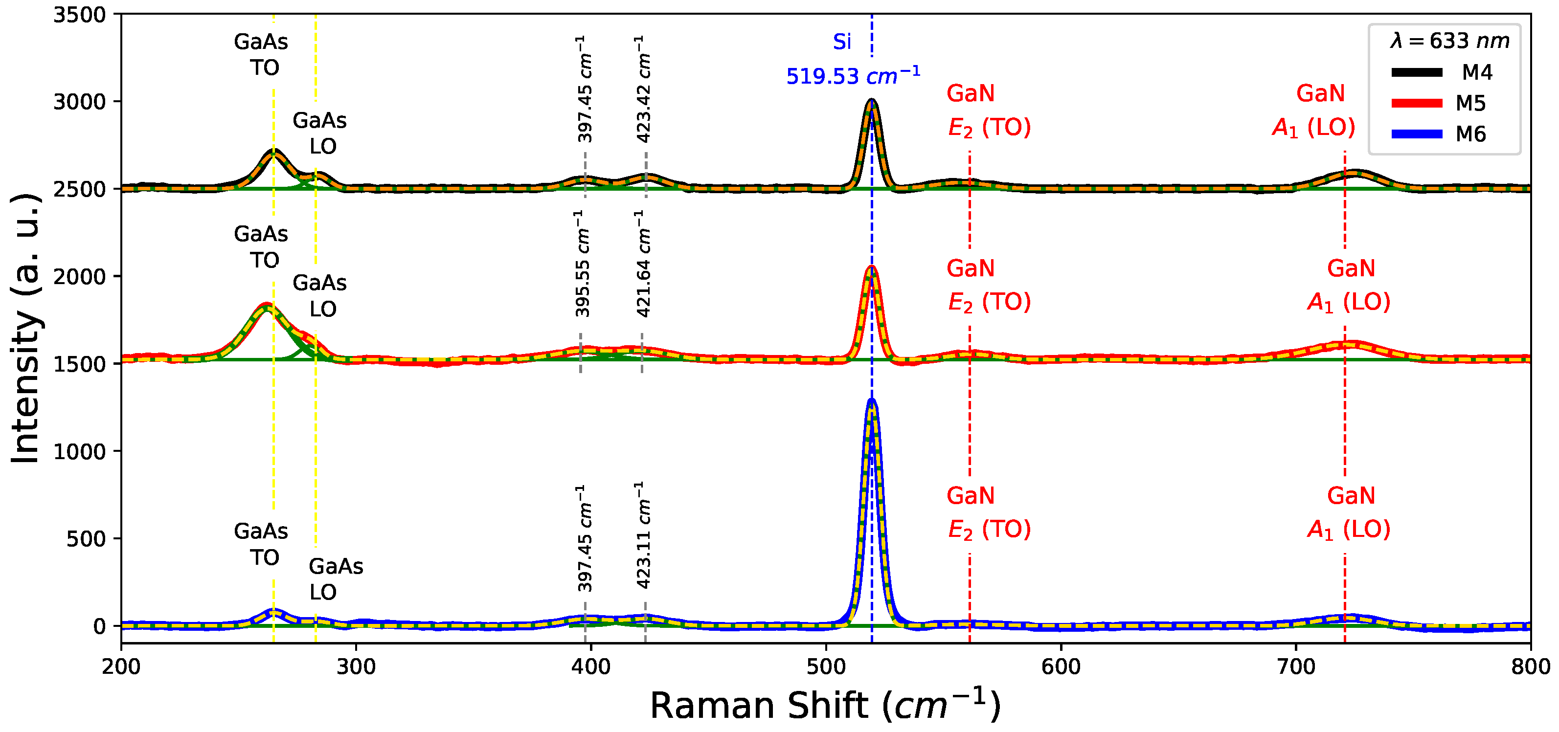
| M4 | 256.18 | 283.86 | 397.45 | 423.42 | 562.14 | 720.77 |
| M5 | 262.2 | 280.0 | 395.96 | 421.46 | 557.39 | 723.98 |
| M6 | 264.9 | 284.8 | 397.45 | 423.11 | 561.98 | 720.56 |
Disclaimer/Publisher’s Note: The statements, opinions and data contained in all publications are solely those of the individual author(s) and contributor(s) and not of MDPI and/or the editor(s). MDPI and/or the editor(s) disclaim responsibility for any injury to people or property resulting from any ideas, methods, instructions or products referred to in the content. |
© 2023 by the authors. Licensee MDPI, Basel, Switzerland. This article is an open access article distributed under the terms and conditions of the Creative Commons Attribution (CC BY) license (https://creativecommons.org/licenses/by/4.0/).
Share and Cite
Valdez-Torija, E.A.; Coyopol, A.; García-Salgado, G.; Romano-Trujillo, R.; Morales-Ruiz, C.; Rosendo-Andrés, E.; Vásquez-Agustín, M.A.; Gracia-Jiménez, J.M.; Galeazzi-Isasmendi, R.; Morales-Morales, F. Study of Nitridation Effect on Structural, Morphological, and Optical Properties of GaAs Film Growth on Silicon Substrates via Close Space Vapor Transport Technique. Crystals 2023, 13, 613. https://doi.org/10.3390/cryst13040613
Valdez-Torija EA, Coyopol A, García-Salgado G, Romano-Trujillo R, Morales-Ruiz C, Rosendo-Andrés E, Vásquez-Agustín MA, Gracia-Jiménez JM, Galeazzi-Isasmendi R, Morales-Morales F. Study of Nitridation Effect on Structural, Morphological, and Optical Properties of GaAs Film Growth on Silicon Substrates via Close Space Vapor Transport Technique. Crystals. 2023; 13(4):613. https://doi.org/10.3390/cryst13040613
Chicago/Turabian StyleValdez-Torija, Eduardo Alejandro, Antonio Coyopol, Godofredo García-Salgado, Román Romano-Trujillo, Crisóforo Morales-Ruiz, Enrique Rosendo-Andrés, Marco Antonio Vásquez-Agustín, Justo Miguel Gracia-Jiménez, Reina Galeazzi-Isasmendi, and Francisco Morales-Morales. 2023. "Study of Nitridation Effect on Structural, Morphological, and Optical Properties of GaAs Film Growth on Silicon Substrates via Close Space Vapor Transport Technique" Crystals 13, no. 4: 613. https://doi.org/10.3390/cryst13040613
APA StyleValdez-Torija, E. A., Coyopol, A., García-Salgado, G., Romano-Trujillo, R., Morales-Ruiz, C., Rosendo-Andrés, E., Vásquez-Agustín, M. A., Gracia-Jiménez, J. M., Galeazzi-Isasmendi, R., & Morales-Morales, F. (2023). Study of Nitridation Effect on Structural, Morphological, and Optical Properties of GaAs Film Growth on Silicon Substrates via Close Space Vapor Transport Technique. Crystals, 13(4), 613. https://doi.org/10.3390/cryst13040613