Abstract
As important third-generation semiconductors, wurtzite III nitrides have strong spontaneous and piezoelectric polarization effects. They can be used to construct multifunctional polar heterojunctions or quantum structures with other emerging two-dimensional (2D) semiconductors. Here, we investigate the polarization effect of GaN on the interfacial charge transfer and electronic properties of GaN/MoS2 polar heterojunctions by first-principles calculations. From the binding energy, the N-polarity GaN/MoS2 heterojunctions show stronger structural stability than the Ga-polarity counterparts. Both the Ga-polarity and N-polarity GaN/MoS2 polar heterojunctions have type-II energy band alignments, but with opposite directions of both the built-in electric field and interfacial charge transfer. In addition, their heterostructure types can be effectively modulated by applying in-plane biaxial strains on GaN/MoS2 polar heterojunctions, which can undergo energy band transitions from type II to type I. As a result, it provides a feasible solution for the structural design and integrated applications of hybrid 3D/2D polar heterojunctions in advanced electronics and optoelectronics.
1. Introduction
Due to the electronegativity difference of atoms, the positive and negative charges are separated in the wurtzite GaN and nitride semiconductors, which have extensive applications in next-generation RF power amplifiers, power switches, light-emitting diodes, lasers, solar cells, photodetectors, and integrated circuits [1,2,3,4,5,6,7,8]. GaN has two distinct polarities called Ga-polarity and N-polarity along the [0001] and [000-1] directions, respectively. The lack of inversion symmetry in GaN gives rise to a large spontaneous polarization charge of ~0.029 C/m2 and a polarization electric field of ~107 V/cm. The surface polarity of GaN dramatically influences surface energies, growth modes, susceptibilities to chemicals, electric charge dynamics, and so on. Its strong polarization greatly influences the GaN-based electronic and optoelectronic performances by energy band tilt and charge separation or accumulation at the polar heterointerfaces, such as AlGaN/GaN, InGaN/GaN and metal-polar semiconductor Schottky interfaces.
With regard to the developing trend of 3D-to-2D miniaturization and multifunctional integration, 2D semiconductors beyond graphene have become a research hotspot due to their unique electrical, photonic, and mechanical performances [9]. There is a large number of 2D semiconductor materials widely used in field-effect transistors and optoelectronic devices, such as transition metal dichalcogenides (TMDs) [10,11], black phosphorus (BP) [12], silicene [13], and III-VI layered materials [14]. Among them, 2D TMDs show tunable bandgaps from 1.1 eV (MoTe2) to 2.0 eV (WS2) for highly visible and near-infrared optoelectronic response [15,16]. Meanwhile, 2D TMDs have excellent flexibility and high carrier mobility, enabling ultrathin and lightweight, flexible electronic applications [17].
Currently, 2D semiconductors are used as potential building blocks to form low-dimensional semiconductor heterostructures for improving electronic and optical performances [18,19,20,21,22], such as MoS2/graphene [23], MoS2/WS2 [24], MoS2/WSe2 [25], and α-In2Se3/MoS2 [26]. In comparison with 2D/2D architecture, mixed-dimensional 3D/2D heterostructures have greater application potential in integrating with conventional semiconductors, such as Si, GaAs, GaN, etc. In order to obtain the full utilization of the broad optical spectrum, the integration of 2D TMDs with 3D wide-bandgap GaN is a feasible solution, such as MoS2/GaN, MoSe2/GaN, etc. [27,28]. Desai et al. grew a homogeneous MoS2 layer on a GaN substrate to produce a MoS2/GaN vertical heterojunction with a type-II energy band arrangement, and showed excellent electrical rectifying characteristic and photovoltaic responsivity under monochromatic illumination [29]. Yang et al. prepared triangular MoS2 monolayers on GaN substrates by CVD, which exhibited an indirect bandgap of MoS2/GaN with broadband optical absorption [30]. The type-II band alignment of MoS2/GaN helps to effectively separate the photogenerated electrons and holes, which demonstrated unique advantages for broadband photodetectors and high-efficiency solar cells [31,32,33]. Theoretically, by first-principles calculations, Gao et al. reported the MoS2/2D GaN van der Waals (vdW) heterostructures possess a direct gap about 1.79 eV with type-II band alignment and excellent optical absorbance of approximately ~5.5 × 105 cm−1 [34]. It was found that changing interlayer coupling and applying external electric fields can effectively and broadly engineer its band gap and optical properties. However, 2D GaN is difficult to synthesize experimentally and does not have strong out-of-plane polarity like 3D GaN for practical polarization modulation. In addition, Sung et al. performed density-generalized function theory calculations to investigate the interfacial structures between 2D-MoS2 and 3D-GaN [35]. It was reported that the surface states and electrical characteristics of the 2D/3D MoS2/GaN heterostructures could be controlled by the surface terminations of GaN. However, other types of band alignments are actually needed to control carrier distribution, charge transfer, and spatial confinement of 2D/3D GaN/MoS2 heterostructures. To date, there is still a lack of effective means, such as GaN polarity flip and strain modulation for optical emission, electrooptic conversion, and advanced energy-harvesting applications.
In this work, we constructed two types of GaN/MoS2 (I) and (II) polar heterojunctions by manipulating the Ga-polarity and N-polarity of GaN to investigate the interfacial interactions and electronic band structures between MoS2 and GaN, respectively. It is found that both of them are type-II energy band-aligned, with the heterojunction bandgaps of 0.87 eV and 1.53 eV for GaN/MoS2 (I) and GaN/MoS2 (II), respectively. Based on the differential charge density analysis, the negative charges are transferred in the opposite directions, from GaN to MoS2 in Ga-polarity GaN/MoS2 (I) and from MoS2 to GaN in N-polarity GaN/MoS2 (II), respectively. Correspondingly, the net charge transfer amounts of 0.036 e and 0.088 e demonstrates that the interfacial interaction is stronger in GaN/MoS2 (II) than that in GaN/MoS2 (I), which is consistent with the lower binding energy of GaN/MoS2 (II). In addition, piezoelectric polarization of GaN has been utilized by in-plane biaxial strains to modulate the energy band configurations of GaN/MoS2 heterojunctions, which can undergo an energy band transition from type II to type I. Therefore, the polarization modulation of GaN/MoS2 heterojunctions provides a facile strategy for interfacial charge transfer and energy band configurations in 3D/2D polar semiconductors and device applications.
2. Computation Methods
Based on the first-principles density functional theory (DFT), our computational simulations were implemented by the Vienna ab initio simulation package (VASP) [36,37]. The heterojunction structure models were constructed by Materials Studio (MS) software. The interactions between the core and valence electrons were described by using the projector-augmented wave (PAW) method [38]. The Perdew−Burke−Ernzerhof version of the generalized gradient approximation (PBE-GGA) was selected as the electron exchange–correlation interaction functional [39], which was used for structural optimization and static self-consistent calculations. The strongly constrained and appropriately normed semilocal density (SCAN) functional was utilized to calculate the semiconductor bandgaps and electronic band structures [40]. Generally, it is efficient for accurate modeling of electronic structures of layered materials in high-throughput calculations [41]. The energy cutoff for the plane–wave basis expansion was set to be 500 eV. The Brillouin zone was sampled with a 12 × 12 × 1 Monkhorst−Pack grid. The convergence criteria of electronic and geometric optimization were 10−6 eV and 0.01 eV/Å. The algorithm selection for electronic optimization was normal. The Brillouin zone integration was performed by the Gaussian smearing (ISMEAR = 0) method with the smearing width (SIGMA) of 0.05 eV. The DFT-D3 method was used to correct interlayer vdW interactions between the MoS2 monolayer and the GaN surface [42,43,44,45]. The vacuum space of 15 Å was adopted to avoid interactions between the periodic sheets. During the 3D/2D construction of GaN/MoS2 heterostructures, the dangling bonds at the bottom surface of GaN layer were passivated by H atoms.
During our calculations, the initially established GaN/MoS2 heterostructures were geometrically optimized by the lattice constants and the layer spacing. The optimized structure models were then subjected to static self-consistent calculations to obtain the charge density files. Subsequently, the SCAN generalization was used to increase the K-point grids to calculate the density of states, and the K path was set to G-M-K-G for the energy band calculation.
3. Results and Discussion
3.1. Polarity Configurations on Electronic Band Structures of GaN/MoS2 vdW Heterostructures
As for the geometric structures of MoS2 and GaN in Figure 1a, the 2D MoS2 monolayer in the order of S-Mo-S arrangement has a hexagonal crystalline structure with the optimized lattice constants of a = b = 3.18 Å, while 3D wurtzite GaN has the same hexagonal structure with the optimized lattice constants of a = b = 3.21 Å. Their lattice mismatch between MoS2 and GaN is only 0.9%, which facilitates 3D/2D heteroepitaxy for building GaN/MoS2 heterostructures. Considering the spontaneous polarization effect of the GaN polar semiconductor along z axis, Ga-polarity and N-polarity GaN/MoS2 heterojunctions have been constructed in the I and II stacking configurations. As shown in Figure 1b, the Ga face of GaN layer is contacted with the S atoms of MoS2 monolayer at the GaN/MoS2 (I) heterointerface, and, correspondingly, the N face of GaN layer is contacted with the S atoms at the GaN/MoS2 (II) heterointerface, respectively. The lattice constants and interlayer equilibrium distances of the optimized GaN/MoS2 unit cells are similar with a = b = 3.20 Å and d = 2.35 Å in configuration I, and a = b = 3.19 Å and d = 2.35 Å in configuration II, respectively. In order to quantitatively characterize the structural stability of GaN/MoS2 heterojunctions, the binding energy has been calculated as follows,
where , and are the total energies of the GaN/MoS2 vdW heterostructures, monolayer MoS2 and GaN, respectively. Both GaN/MoS2 (I) and GaN/MoS2 (II) have negative binding energies of −0.395 eV and −0.407 eV, respectively. It demonstrates that it can form stable vdW heterostructures between MoS2 and GaN. Comparatively, MoS2 monolayer has a stronger interfacial interaction with the N face of GaN than that with the Ga face of GaN.

Figure 1.
(a) Top and side views of 3 × 3 MoS2 monolayer and 3 × 3 GaN supercells. (b) Side views of GaN/MoS2 (I) and (II) heterostructures based on Ga-polarity and N-polarity surfaces, respectively.
Figure 2 shows the projected band structures and local density of states (LDOS) of MoS2, GaN, and the GaN/MoS2 (I) and (II) heterojunctions. MoS2 has a direct bandgap of 1.75 eV with both the conduction band minimum (CBM) and valence band maximum (VBM) locating at K point, as shown in Figure 2a, which is consistent with the reported experimental values [46]. In Figure 2b, GaN shows a direct bandgap of 2.4 eV at Γ point calculated by the SCAN method, which is lower than the calculated 3.4 eV by the HSE06 method. According to LDOS diagrams, both the CBM and VBM of the isolated MoS2 and GaN are mainly contributed by the Mo and N states, respectively.
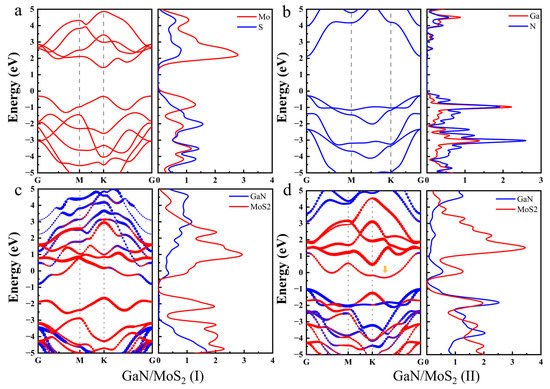
Figure 2.
Band structures and local density of states of (a) MoS2, (b) GaN, (c) GaN/MoS2 (I), and (d) GaN/MoS2 (II) heterostructures, respectively. The Fermi level is set as the zero reference.
As shown in Figure 2c,d, the energy bands of the GaN/MoS2 heterojunctions are not a simple superposition of those of each GaN and MoS2. The blue and red lines represent the electronic energy band weights of GaN and MoS2, respectively. Due to the opposite polarity of GaN, the GaN/MoS2 (I) and (II) heterojunctions have different indirect bandgaps of 0.87 eV and 1.53 eV, respectively. The CBM and VBM of GaN/MoS2 (I) heterojunction is contributed by GaN and MoS2, respectively. In contrast, the CBM and VBM of GaN/MoS2 (II) heterojunction is contributed by MoS2 and GaN, respectively. Consequently, both of them exhibit type-II band alignment, but the energy bands between MoS2 and GaN can be reversed from Ga polarity to N polarity. Moreover, there exists an energy level located in the bandgap of the GaN/MoS2 (II) heterojunction, as indicated by the orange arrow in Figure 2d. In combination with the LDOS analysis, it is contributed by both of MoS2 and GaN, which may arise from the interfacial hybridization of the N-polarity surface state of GaN with MoS2 [35]. However, the hybridization state is not observed in the Ga-polarity GaN/MoS2 (II) configuration, which is due to the surface dangling bonds of the Ga-polarity GaN bonded with the MoS2.
3.2. Charge Transfer Mechanisms of GaN/MoS2 vdW Heterostructures
In addition to modulating the electronic band structures, GaN polarity also has a direct impact on the charge transfer processes. Figure 3 presents the average planar electrostatic potentials of the MoS2 monolayer, GaN, and GaN/MoS2 (I) and (II) heterojunctions along the z direction. The black dashed line represents the energy level of a stationary electron in the vacuum () and the red dashed line represents the Fermi level of the corresponding systems (. The work function () is defined as follows:
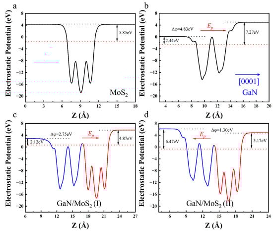
Figure 3.
Planar average electrostatic potentials of (a) MoS2 monolayer, (b) GaN, (c) GaN/MoS2 (I), and (d) GaN/MoS2 (II) heterostructures along z-direction, respectively. In (c) and (d), the blue and red parts of the electrostatic potential curves correspond to GaN and MoS2, respectively. The red and blue arrows indicate the directions of the polarization-induced electric fields and [0001] polarity axis, respectively. The vacuum levels and Fermi levels are marked with black and red dashed lines, respectively.
It is a critical parameter to get a further understanding on the physical mechanisms of the charge transfer at GaN/MoS2 heterojunction interfaces. As shown in Figure 3a, the work function of MoS2 monolayer is 5.85 eV. However, due to the spontaneous polarization induced by GaN layer, the different work functions at the left and right ends of the z-axis direction are 2.44 and 7.27 eV for GaN, 2.12 and 4.87 eV for GaN/MoS2 (I), and 6.47 and 5.17 eV for GaN/MoS2 (II) as shown in Figure 3b–d, respectively. There exists the electrostatic potential difference () between the upper and lower surfaces of GaN, GaN/MoS2 (I), and GaN/MoS2 (II) heterojunctions. As presented by the interval of the black dashed lines in Figure 3b–d, the electrostatic potential differences are 4.83 eV between Ga-polarity and N-polarity surfaces of GaN, 2.75 eV for GaN/MoS2 (I) and 1.3 eV for GaN/MoS2 (II) configurations, respectively. It hence induces a polarization-induced electric field () according to the following equation,
where e and d are the elementary charge and the layer thickness of semiconducting materials or heterostructures, respectively. Correspondingly, the calculated polarization-induced electric fields are 0.68 V/Å, 0.23 V/Å, and 0.11 V/Å for GaN, GaN/MoS2 (I), and GaN/MoS2 (II), respectively. In particular, due to the polarity reversal of GaN/MoS2 (I) and GaN/MoS2 (II) configurations, their internal polarization-induced electric fields are in the opposite directions. In addition, the electrostatic potential differences of both configurations are lower than the difference of the isolated GaN. It demonstrates that the polarization strength in GaN has been attenuated by an interfacial depolarization effect. As a result, GaN polarity plays a great role on both the interfacial potential and internal electric field of GaN-based polar heterostructures.
Based on the above results of band structures and electrostatic potentials, Figure 4a,b shows the band alignment schematics of GaN/MoS2 heterojunctions before contact and after contact in I and II configurations, respectively. The vacuum energy level is set to be zero as a reference. Once the GaN/MoS2 heterostructures are formed, charge transfer will happen at the interface of GaN and MoS2, thus achieving the same Fermi energy levels. Correspondingly, it also leads to the formation of a built-in electric field at the GaN/MoS2 heterojunctions, which could hinder the further diffusion of electrons and holes, and eventually reach equilibrium. As compared with MoS2, the energy bands of GaN shift downward and upward in the contacted GaN/MoS2 (I) and GaN/MoS2 (II) configurations in Figure 4a,b, respectively. Both the CBM and VBM of GaN are lower than those of MoS2 in the contacted GaN/MoS2 (I) and vice versa in the contacted GaN/MoS2 (II). As a result, these two configurations have type-II band alignments, which could boost the spatial charge separation and reduce electron-hole recombination efficiency. Due to their opposite directions in terms of charge transfer and built-in electric field, the type and number of charge separation between GaN and MoS2 can be directly controlled by adjusting the intrinsic polarization of GaN.
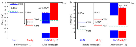
Figure 4.
Schematic diagrams of energy band configurations of (a) GaN/MoS2 (I) and (b) GaN/MoS2 (II) heterojunctions before contact and after contact, respectively. The blue and red parts are GaN and MoS2, respectively. The Fermi energy levels are indicated by green dashed lines.
In order to quantitatively analyze the interfacial charge transfer between GaN and MoS2 during the formation of heterojunctions, the charge density difference (Δρ) is calculated according to the following equation,
where ρ(GaN/MoS2), ρ(GaN) and ρ(MoS2) denote the charge density of the GaN/MoS2, the freestanding GaN and MoS2 monolayer, respectively. Figure 5 shows the plane-averaged charge density differences of GaN/MoS2 (I) and GaN/MoS2 (II) along the z direction. The blue and red colors indicate the charge accumulation and depletion, respectively. In Figure 5c,d the red dashed lines represent the GaN/MoS2 interface boundaries. GaN and MoS2 correspond to the left and right sides of the interface boundaries, respectively. As shown in Figure 5a,c, the charges are depleted in GaN and accumulated in MoS2 at the interface of GaN/MoS2 (I). However, the charge depletion and accumulation are the opposite at the interface of GaN/MoS2 (II) in Figure 5b,d. These results on charge transfer are consistent with their band alignments in Figure 4. In addition, the net charge transfer amounts can be evaluated by the difference between the charge accumulation and depletion at the heterointerface. They are 0.036 e and 0.088 e in GaN/MoS2 (I) and (II) configurations, respectively. This demonstrates that the interfacial interaction is stronger in GaN/MoS2 (II) than that in GaN/MoS2 (I), which is consistent with the lower binding energy of GaN/MoS2 (II).
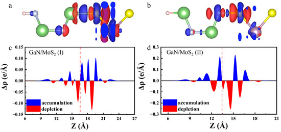
Figure 5.
Plane-averaged charge density differences of (a) and (c) GaN/MoS2 (I), (b) and (d) GaN/MoS2 (II) heterostructures in 3D spatial distributions and along the z−direction, respectively. In (c) and (d), the red dashed lines represent the GaN/MoS2 interface boundaries. GaN and MoS2 correspond to the left and right sides of the interface boundaries, respectively.
3.3. Strain Modulation on the Electronic Band Structures of GaN/MoS2 vdW Heterostructures
Strain engineering is of great significance to further tailor the electronic structures and band alignments of 2D polar semiconductors and heterostructures. It can be used to modulate the polarization strength based on the piezoelectric polarization effect. Here, the in-plane biaxial strain has been applied to investigate the energy bands of GaN/MoS2 polar heterojunctions. The in-plane biaxial strain (ε) is defined as
where and are the lattice constants with and without strain, respectively. Figure 6 shows the projected energy bands of the GaN/MoS2 (I) and GaN/MoS2 (II) polar heterojunctions by tuning the in-plane biaxial strains from −10% (compressive) to 10% (tensile). The blue and red colors indicate the contributions of GaN and MoS2, respectively. For the strained GaN/MoS2 (I) polar heterojunction in Figure 6a, MoS2 exhibits indirect bandgaps, with VBM at K point and CBM between K and G points under compressive strains, in contrast with CBM at K point and VBM between K and G points under tensile strains. Meanwhile, GaN keeps direct band gaps with both VBM and CBM located at G point under strains from −10% to 10%. When changing from tensile strains to compressive strains, the energy bands of GaN shift significantly upward, and its band gap values decrease gradually. For the strained GaN/MoS2 (II) polar heterojunction in Figure 6, MoS2 shows a direct-to-indirect band gap transition from compressive strains (−6%, −10%) to tensile strains (6%, 10%), while GaN remains a direct band gap. In contrast to that of GaN/MoS2 (I), a new hybridized state appeared in the band gap of GaN/MoS2 (II) as indicated by the orange arrow in Figure 6b. It is due to the electron orbital interactions between surface N atoms of N-polarity GaN and MoS2. When applying the biaxial tensile strains, the hybridized state gradually overlaps with the downshifted conduction bands of MoS2.
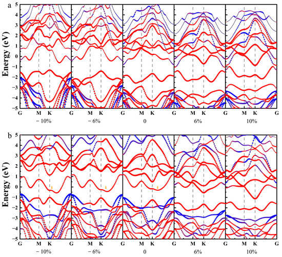
Figure 6.
Projected band structures of (a) GaN/MoS2 (I) and (b) GaN/MoS2 (II) heterostructures under biaxial strains of −10%, −6%, 0%, 6%, and 10%, in which the red and blue colors indicates the contributions of MoS2 and GaN, respectively.
In order to further clarify the energy band alignment relationship of the GaN/MoS2 heterojunctions under different strains, Figure 7 presents the CBMs and VBMs of MoS2 at K point and GaN at G point as a function of biaxial strains. All the CBM and VBM values of both MoS2 and GaN decrease under tensile strains and increase under compressive strains in GaN/MoS2 (I) and (II) configurations. In addition, the energy band alignments between MoS2 and GaN can be transformed from type II to type I as applying biaxial tensile strains. The controllable band transformation is favorable for charge separation, recombination, redistribution, and fast transfer processes in 3D/2D polar heterointerfaces. Comparatively, the required tensile strain for the band transformation is less in GaN/MoS2 (II) than that in GaN/MoS2 (I). As a result, the biaxial strains not only modulate the electronic structures of each GaN and MoS2 layer, but also play a significant role on the interfacial band hybridization and band alignment relationship of GaN/MoS2 polar heterojunction.
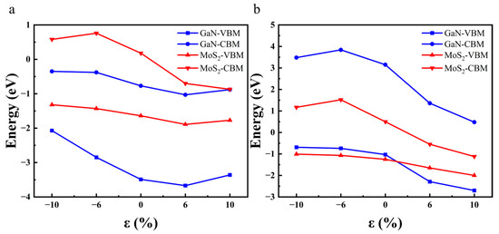
Figure 7.
Band alignments of (a) GaN/MoS2 (I) and (b) GaN/MoS2 (II) heterostructures under biaxial strains of −10%, −6%, 0%, 6%, and 10%, respectively.
4. Conclusions
In summary, we have constructed 3D/2D GaN/MoS2 polar heterojunctions to investigate the interfacial interactions and electronic band structures by polarization modulation. It demonstrates that the interfacial interaction is stronger in GaN/MoS2 (II) than that in GaN/MoS2 (I), as indicated by both the binding energy and net charge transfer amount. Both GaN/MoS2 (I) and GaN/MoS2 (II) have type-II band alignments, which could boost the spatial charge separation and reduce electron-hole recombination efficiency. By flipping the polarization directions of GaN, the type and number of transferred charges between GaN and MoS2 can be directly controlled by the polarization-induced electric field. In addition, the energy band alignments between MoS2 and GaN can be transformed from type II to type I as applying biaxial tensile strains. Thus, the polarization modulation is an effective way by which to control carrier distribution and spatial confinement for 3D/2D polar semiconductors and device applications.
Author Contributions
F.T., data curation, formal analysis, investigation, methodology, validation, writing—original draft; D.K., data curation, formal analysis, investigation, methodology, validation, writing—original draft. P.Q., investigation, methodology, validation. H.L., investigation, methodology, validation. X.Z. (Xiaoli Zhu), investigation, methodology, validation. H.W., investigation, methodology, validation; Y.S., investigation, methodology, validation. H.C., validation, resources, supervision; X.Z. (Xinhe Zheng), funding acquisition, resources, supervision; M.P., conceptualization, funding acquisition, project administration, resources, supervision, writing—review and editing. All authors have read and agreed to the published version of the manuscript.
Funding
This research was financially supported by the Beijing Natural Science Foundation (grant numbers 4222071), National Key R&D Program of China (grant number 2018YFA0703700), Fundamental Research Funds for the Central Universities (grant numbers FRF-BR-20-02A, FRF-TP-19-044A2, FRF-TP-20-016A2), National Natural Science Foundation of China (grant numbers 51402064), Student Research Training Project (grant number 202021010), Youth Innovation Promotion Association of Chinese Academy of Sciences (grant number 2015387).
Data Availability Statement
The data that support the findings of this study are available from the corresponding author upon reasonable request.
Conflicts of Interest
The authors declare no conflict of interest.
References
- Mishra, U.K.; Shen, L.; Kazior, T.E.; Wu, Y.F. GaN-based RF power devices and amplifiers. Proc. IEEE 2008, 96, 287–305. [Google Scholar] [CrossRef]
- Chen, K.J.; Häberlen, O.; Lidow, A.; Tsai, C.L.; Ueda, T.; Uemoto, Y.; Wu, Y. GaN-on-Si power technology: Devices and applications. IEEE Trans. Electron Devices 2017, 64, 779–795. [Google Scholar] [CrossRef]
- Khan, A.; Balakrishnan, K.; Katona, T. Ultraviolet light-emitting diodes based on group three nitrides. Nat. Photonics 2008, 2, 77–84. [Google Scholar] [CrossRef]
- Lee, K.; Wu, Z.; Chen, Z.; Ren, F.; Pearton, S.J.; Rinzler, A.G. Single wall carbon nanotubes for p-type ohmic contacts to GaN light-emitting diodes. Nano Lett. 2004, 4, 911–914. [Google Scholar] [CrossRef]
- Choi, H.J.; Johnson, J.C.; He, R.; Lee, S.K.; Kim, F.; Pauzauskie, P.; Goldberger, J.; Saykally, R.J.; Yang, P. Self-organized GaN quantum wire UV lasers. J. Phys. Chem. B 2003, 107, 8721–8725. [Google Scholar] [CrossRef]
- Wang, Y.; Zheng, D.; Li, L.; Zhang, Y. Enhanced efficiency of flexible GaN/perovskite solar cells based on the piezo-phototronic effect. ACS Appl. Energy Mater. 2018, 1, 3063–3069. [Google Scholar] [CrossRef]
- Li, J.; Xi, X.; Lin, S.; Ma, Z.; Li, X.; Zhao, L. Ultrahigh sensitivity graphene/nanoporous GaN ultraviolet photodetectors. ACS Appl. Mater. Interfaces 2020, 12, 11965–11971. [Google Scholar] [CrossRef]
- Tchernycheva, M.; Messanvi, A.; de Luna Bugallo, A.; Jacopin, G.; Lavenus, P.; Rigutti, L.; Zhang, H.; Halioua, Y.; Julien, F.H.; Eymery, J.; et al. Integrated photonic platform based on InGaN/GaN nanowire emitters and detectors. Nano Lett. 2014, 14, 3515–3520. [Google Scholar] [CrossRef]
- Gupta, A.; Sakthivel, T.; Seal, S. Recent development in 2D materials beyond graphene. Prog. Mater. Sci. 2015, 73, 44–126. [Google Scholar] [CrossRef]
- Zhang, Y.; Yao, Y.; Sendeku, M.G.; Yin, L.; Zhan, X.; Wang, F.; Wang, Z.; He, J. Recent progress in CVD growth of 2D transition metal dichalcogenides and related heterostructures. Adv. Mater. 2019, 31, 1901694. [Google Scholar] [CrossRef]
- Jariwala, D.; Sangwan, V.K.; Lauhon, L.J.; Marks, T.J.; Hersam, M.C. Emerging device applications for semiconducting two-dimensional transition metal dichalcogenides. ACS Nano 2014, 8, 1102–1120. [Google Scholar] [CrossRef] [PubMed]
- Li, L.; Yu, Y.; Ye, G.J.; Ge, Q.; Ou, X.; Wu, H.; Feng, D.; Chen, X.; Zhang, Y. Black phosphorus field-effect transistors. Nat. Nanotechnol. 2014, 9, 372–377. [Google Scholar] [CrossRef] [PubMed]
- Tao, L.; Cinquanta, E.; Chiappe, D.; Grazianetti, C.; Fanciulli, M.; Dubey, M.; Molle, A.; Akinwande, D. Silicene field-effect transistors operating at room temperature. Nat. Nanotechnol. 2015, 10, 227–231. [Google Scholar] [CrossRef]
- Yang, Z.; Hao, J. Recent progress in 2D layered III–VI semiconductors and their heterostructures for optoelectronic device applications. Adv. Mater. Technol. 2019, 4, 1900108. [Google Scholar] [CrossRef]
- Chang, Y.H.; Zhang, W.; Zhu, Y.; Han, Y.; Pu, J.; Chang, J.K.; Hsu, W.; Huang, J.; Hsu, C.; Chiu, M.; et al. Monolayer MoSe2 grown by chemical vapor deposition for fast photodetection. ACS Nano 2014, 8, 8582–8590. [Google Scholar] [CrossRef] [PubMed]
- Xie, Y.; Zhang, B.; Wang, S.; Wang, D.; Wang, A.; Wang, Z.; Yu, H.; Zhang, H.; Chen, Y.; Zhao, M.; et al. Ultrabroadband MoS2 photodetector with spectral response from 445 to 2717 nm. Adv. Mater. 2017, 29, 1605972. [Google Scholar] [CrossRef]
- Malakar, P.; Thakur, M.S.H.; Nahid, S.M.; Islam, M.M. Data-Driven Machine Learning to Predict Mechanical Properties of Monolayer Transition-Metal Dichalcogenides for Applications in Flexible Electronics. ACS Appl. Nano Mater. 2022, 5, 16489–16499. [Google Scholar] [CrossRef]
- Geim, A.K.; Grigorieva, I.V. Van der Waals heterostructures. Nature 2013, 499, 419–425. [Google Scholar] [CrossRef]
- Coy Diaz, H.; Avila, J.; Chen, C.; Addou, R.; Asensio, M.C.; Batzill, M. Direct observation of interlayer hybridization and Dirac relativistic carriers in graphene/MoS2 van der Waals heterostructures. Nano Lett. 2015, 15, 1135–1140. [Google Scholar] [CrossRef]
- Novoselov, K.S.; Mishchenko, A.; Carvalho, O.A.; Castro Neto, A.H. 2D materials and van der Waals heterostructures. Science 2016, 353, aac9439. [Google Scholar] [CrossRef]
- Pierucci, D.; Henck, H.; Avila, J.; Balan, A.; Naylor, C.H.; Patriarche, G.; Dappe, Y.J.; Silly, M.G.; Sirotti, F.; Johnson, A.T.C.; et al. Band alignment and minigaps in monolayer MoS2-graphene van der Waals heterostructures. Nano Lett. 2016, 16, 4054–4061. [Google Scholar] [CrossRef]
- Le, P.T.T.; Hieu, N.N.; Bui, L.M.; Phuc, H.V.; Hoi, B.D.; Amin, B.; Nguyen, C.V. Structural and electronic properties of a van der Waals heterostructure based on silicene and gallium selenide: Effect of strain and electric field. Phys. Chem. Chem. Phys. 2018, 20, 27856–27864. [Google Scholar] [CrossRef] [PubMed]
- Bertolazzi, S.; Krasnozhon, D.; Kis, A. Nonvolatile memory cells based on MoS2/graphene heterostructures. ACS Nano 2013, 7, 3246–3252. [Google Scholar] [CrossRef] [PubMed]
- Tongay, S.; Fan, W.; Kang, J.; Park, J.; Koldemir, U.; Suh, J.; Narang, D.S.; Liu, K.; Ji, J.; Li, J.; et al. Tuning interlayer coupling in large-area heterostructures with CVD-grown MoS2 and WS2 monolayers. Nano Lett. 2014, 14, 3185–3190. [Google Scholar] [CrossRef] [PubMed]
- Shim, G.W.; Yoo, K.; Seo, S.B.; Shin, J.; Jung, D.Y.; Kang, I.S.; Ahn, C.W.; Cho, B.J.; Choi, S.Y. Large-area single-layer MoSe2 and its van der Waals heterostructures. ACS Nano 2014, 8, 6655–6662. [Google Scholar] [CrossRef]
- Zhou, B.; Jiang, K.; Shang, L.; Zhang, J.; Li, Y.; Zhu, L.; Gong, S.J.; Hu, Z.; Chu, J. Enhanced carrier separation in ferroelectric In2Se3/MoS2 van der waals heterostructure. J. Mater. Chem. C 2020, 8, 11160–11167. [Google Scholar] [CrossRef]
- Chen, Z.; Liu, H.; Chen, X.; Chu, G.; Chu, S.; Zhang, H. Wafer-size and single-crystal MoSe2 atomically thin films grown on GaN substrate for light emission and harvesting. ACS Appl. Mater. Interfaces 2016, 8, 20267–20273. [Google Scholar] [CrossRef]
- Yang, G.; Gu, Y.; Yan, P.; Wang, J.; Xue, J.; Zhang, X.; Lu, N.; Chen, G. Chemical vapor deposition growth of vertical MoS2 nanosheets on p-GaN nanorods for photodetector application. ACS Appl. Mater. Interfaces 2019, 11, 8453–8460. [Google Scholar] [CrossRef]
- Desai, P.; Ranade, A.K.; Shinde, M.; Todankar, B.; Mahyavanshi, R.D.; Tanemura, M.; Kalita, G. Growth of uniform MoS2 layers on free-standing GaN semiconductor for vertical heterojunction device application. J. Mater. Sci. Mater. Electron. 2020, 31, 2040–2048. [Google Scholar] [CrossRef]
- Yang, G.; Ding, Y.; Lu, N.; Xie, F.; Gu, Y.; Ye, B.; Yao, Y.; Zhang, X.; Huo, X. Insights Into the Two-Dimensional MoS2 Grown on AlGaN (GaN) Substrates by CVD Method. IEEE Photonics J. 2021, 13, 2200105. [Google Scholar] [CrossRef]
- Cao, B.; Ma, S.; Wang, W.; Tang, X.; Wang, D.; Shen, W.; Qiu, B.; Xu, B.; Li, G. Charge Redistribution in Mg-Doped p-Type MoS2/GaN Photodetectors. J. Phys. Chem. C 2022, 126, 18893–18899. [Google Scholar] [CrossRef]
- Zhang, X.; Li, J.; Ma, Z.; Zhang, J.; Leng, B.; Liu, B. Design and integration of a layered MoS2/GaN van der Waals heterostructure for wide spectral detection and enhanced photoresponse. ACS Appl. Mater. Interfaces 2020, 12, 47721–47728. [Google Scholar] [CrossRef] [PubMed]
- Hassan, M.A.; Kim, M.W.; Johar, M.A.; Waseem, A.; Kwon, M.K.; Ryu, S.W. Transferred monolayer MoS2 onto GaN for heterostructure photoanode: Toward stable and efficient photoelectrochemical water splitting. Sci. Rep. 2019, 9, 20141. [Google Scholar] [CrossRef] [PubMed]
- Gao, R.; Liu, H.; Liu, H.; Yang, J.; Yang, F.; Wang, T. Two-dimensional MoS2/GaN van der Waals heterostructures: Tunable direct band alignments and excitonic optical properties for photovoltaic applications. J. Phys. D Appl. Phys. 2019, 53, 095107. [Google Scholar] [CrossRef]
- Sung, D.; Min, K.A.; Hong, S. Investigation of atomic and electronic properties of 2D-MoS2/3D-GaN mixed-dimensional heterostructures. Nanotechnology 2019, 30, 404002. [Google Scholar] [CrossRef]
- Kresse, G.; Furthmüller, J. Efficiency of ab-initio total energy calculations for metals and semiconductors using a plane-wave basis set. Comput. Mater. Sci. 1996, 6, 15–50. [Google Scholar] [CrossRef]
- Blöchl, P.E. Projector augmented-wave method. Phys. Rev. B 1994, 50, 17953. [Google Scholar] [CrossRef]
- Kresse, G.; Joubert, D. From ultrasoft pseudopotentials to the projector augmented-wave method. Phys. Rev. B 1999, 59, 1758. [Google Scholar] [CrossRef]
- Perdew, J.P.; Burke, K.; Ernzerhof, M. Generalized gradient approximation made simple. Phys. Rev. Lett. 1996, 77, 3865. [Google Scholar] [CrossRef]
- Sun, J.; Ruzsinszky, A.; Perdew, J.P. Strongly constrained and appropriately normed semilocal density functional. Phys. Rev. Lett. 2015, 115, 036402. [Google Scholar] [CrossRef]
- Buda, I.G.; Lane, C.; Barbiellini, B.; Ruzsinszky, A.; Sun, J.; Bansil, A. Characterization of thin film materials using SCAN meta-GGA, an accurate nonempirical density functional. Sci. Rep. 2017, 7, 44766. [Google Scholar] [CrossRef] [PubMed]
- Grimme, S. Semiempirical GGA-type density functional constructed with a long-range dispersion correction. J. Comput. Chem. 2006, 27, 1787–1799. [Google Scholar] [CrossRef] [PubMed]
- Grimme, S.; Antony, J.; Ehrlich, S.; Krieg, H. A consistent and accurate ab initio parametrization of density functional dispersion correction (DFT-D) for the 94 elements H-Pu. J. Chem. Phys. 2010, 132, 154104. [Google Scholar] [CrossRef]
- Grimme, S.; Ehrlich, S.; Goerigk, L. Effect of the damping function in dispersion corrected density functional theory. J. Comput. Chem. 2011, 32, 1456–1465. [Google Scholar] [CrossRef] [PubMed]
- Kerber, T.; Sierka, M.; Sauer, J. Application of semiempirical long-range dispersion corrections to periodic systems in density functional theory. J. Comput. Chem. 2008, 29, 2088–2097. [Google Scholar] [CrossRef] [PubMed]
- Mak, K.F.; Lee, C.; Hone, J.; Shan, J.; Heinz, T.F. Atomically thin MoS2: A new direct-gap semiconductor. Phys. Rev. Lett. 2010, 105, 136805. [Google Scholar] [CrossRef]


Disclaimer/Publisher’s Note: The statements, opinions and data contained in all publications are solely those of the individual author(s) and contributor(s) and not of MDPI and/or the editor(s). MDPI and/or the editor(s) disclaim responsibility for any injury to people or property resulting from any ideas, methods, instructions or products referred to in the content. |
© 2023 by the authors. Licensee MDPI, Basel, Switzerland. This article is an open access article distributed under the terms and conditions of the Creative Commons Attribution (CC BY) license (https://creativecommons.org/licenses/by/4.0/).