Article

Type-II GaSe/MoS2 van der Waals Heterojunction for High-Performance Flexible Photodetector

1
School of Materials Science and Engineering, Dalian Jiaotong University, Dalian 116028, China
2
Shenzhen Institute for Quantum Science and Engineering, Southern University of Science and Technology, Shenzhen 518055, China
3
Department of Optoelectronic Science, Harbin Institute of Technology at Weihai, Weihai 264209, China
*
Author to whom correspondence should be addressed.
These authors contributed equally to this work.
Crystals 2023, 13(11), 1602; https://doi.org/10.3390/cryst13111602
Submission received: 25 October 2023 / Revised: 12 November 2023 / Accepted: 16 November 2023 / Published: 20 November 2023
(This article belongs to the Special Issue Emerging Low-Dimensional Materials II)

Abstract

:
In recent years, two-dimensional (2D) type-II van der Waals (vdW) heterojunctions have emerged as promising candidates for high-performance photodetectors. However, direct experimental evidence confirming the enhancement of photoelectric properties by the heterojunction’s type and structure remains scarce. In this work, we present flexible photodetectors based on individual GaSe and MoS2, as well as a vertically stacked type-II GaSe/MoS2 vdW heterojunction on polyethylene terephthalate (PET) substrate. These devices demonstrate outstanding responsivities and rapid response speeds, ensuring stable and repeatable light detection. It is notable that the GaSe/MoS2 heterojunction photodetector exhibits the highest on-off ratio and fastest response speed, attributed to the formation of type-II band alignment. Furthermore, the GaSe/MoS2 heterojunction photodetector maintains robust stability even in a bent state, highlighting remarkable flexibility. This work exemplifies the type-II vdW heterojunctions in enhancing photoelectric properties through direct in-situ experimentation, laying the groundwork for practical applications of 2D flexible photodetectors.

1. Introduction

Photodetectors are widely used in imaging [1,2], sensing [3,4], optical communication [5,6] biomedical application fields [7], etc., and improvement for the performances of photodetectors has attracted extensive attention. Photodetectors fabricated by stacked two-dimensional (2D) van der Waals (vdW) heterostructures is considered as an effective strategy to improve their optoelectronic properties [8,9,10,11,12]. Generally, 2D materials perform distinct optical, electrical and mechanical properties compared to their bulk counterparts. The absence of dangling bonds in various 2D materials allows for the construction of stable heterostructures without the need for precise lattice matching, resulting in excellent and sharp interfaces [13]. The interfacial tunable band alignments of heterostructures are suitable for optimizing the performance of electronic and optoelectronic devices. Notably, type-II band alignments facilitate efficient separation of the photogenerated carriers, extending the lifetime of photoexcited carriers [14,15], and enabling ultrafast charge transfer [16]. Due to the mismatch of the band margin, the photoexcited electron–hole pairs can be effectively separated in the heterojunction, which reduces the probability of the recombination of carriers. Consequently, type-II band alignments offer a promising avenue for enhancing the photoelectric properties of photodetectors. Despite the theoretical advantages, the impact of a type-II vdW heterojunction on improving the performance of a photodetector has not been substantiated by in situ experiments systematically or comprehensively.
Among multifarious 2D materials, GaSe stands out as a typical p-type semiconductor with a direct bandgap of 2.0 eV in its bulk form [17] and the thickness of the monolayer is about 0.93 nm [18]. GaSe exhibits fascinating optoelectronic properties, including high responsivity reached at almost 2200 mA W−1 [19], a low dark current of about 10−11 A [19], nonlinear optical property [20], unique spin polarization [21], etc. Meanwhile, MoS2 is an n-type semiconductor with an indirect bandgap of 1.2 eV in the bulk state [22] and a monolayer thickness of around 0.65 nm [23]. The photodetectors based on MoS2 demonstrate strong light–matter coupling [24], high photoresponsivity exceeding 59 A W−1 [25], a rapid response time of less than 42 μs [25] and a broadband spectral response [26].
Attributed to the formation of type-II band alignment in the GaSe/MoS2 vdW heterojunction, numerous researchers have explored them for photodetection purposes [27,28,29,30,31]. Zou et al. realized the preparation of vertical GaSe/MoS2 heterojunctions by liquid-metal-assisted growth. The resulting self-powered photodetector shows high responsivity of 900 mA W−1 and a fast response speed of 5 ms [30]. Moreover, the escalating demand for portable and wearable applications promotes the development of flexible devices. In view of the excellent mechanical properties of 2D materials, GaSe/MoS2 vdW heterojunctions are considered highly suitable for the fabrication of flexible photodetectors [32,33,34,35]. However, in contrast to the photodetectors based on rigid substrates, those devices based on flexible substrates exhibit lower responsivity [36]. Fabricating high-performance flexible photodetectors remains a substantial challenge.
In this work, we developed a vertically stacked GaSe/MoS2 vdW heterojunction and meticulously examined its properties, confirming the presence of a type-II band alignment. Furthermore, a flexible photodetector based on a vertical GaSe/MoS2 vdW heterojunction was successfully fabricated on the polyethylene terephthalate (PET) substrate. The photoelectric properties for the photodetectors of the GaSe, MoS2, and GaSe/MoS2 heterojunction were systematically evaluated by connecting various Au electrode pairs. A photodetector based on a GaSe/MoS2 vdW heterostructure with type-II band alignment demonstrates superior performance with relatively high responsivity and detectivity of 22.6 mA W−1 and 8.54 × 10⁷ Jones, respectively, along with a rapid response time of 20 ms. In addition, the photodetectors on the PET substrates perform effectively and steadily in the bent state. Our study showcases the efficacy of a type-II GaSe/MoS2 vdW heterojunction for a high-performance flexible photodetector by the in situ experimental manner directly.

2. Materials and Methods

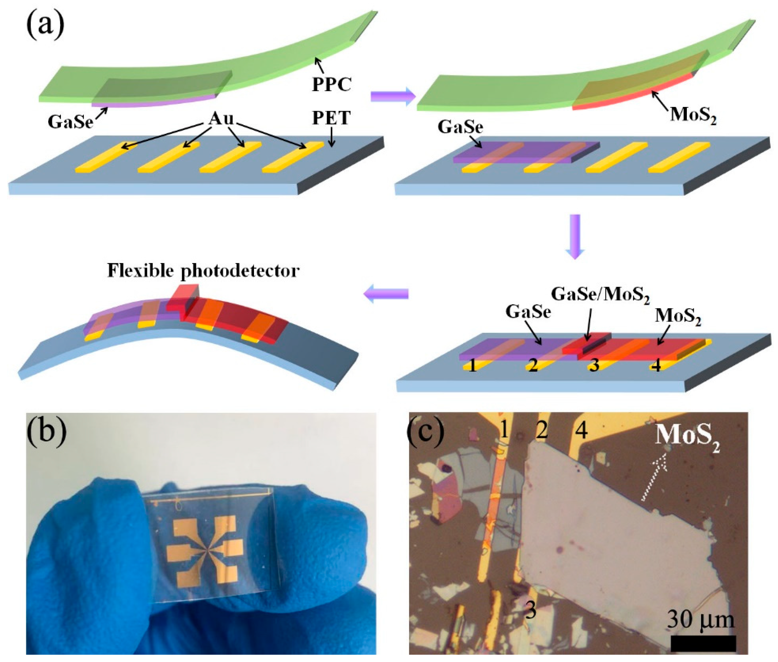
2.1. Preparation of GaSe/MoS2 vdW Heterojunctions

The GaSe and MoS2 nanosheets were mechanically exfoliated from the commercial bulk crystals of high-quality ε-GaSe and MoS2 (Hq Graphene Company, Groningen, Netherlands, purity: >99.9%), respectively. The GaSe and MoS2 layers were then separately transferred onto different SiO2 (300 nm)/Si substrates. Polypropylene carbonate (PPC) was spin-coated on an MoS2 nanosheet, followed by the peeling of PPC and MoS2 from the SiO2/Si substrate. Finally, PPC/MoS2 were stacked onto the previously transferred GaSe nanosheet on the target SiO2/Si substrate. The sample was then immersed in acetone for a few minutes to remove PPC, and the fabrication of vertically stacked GaSe/MoS2 vdW heterojunction was realized.

2.2. Fabrication of Flexible Photodetectors

Similar to the steps above, the flexible photodetector based on the GaSe/MoS2 heterojunction can be obtained by transferring the sample onto a PET target substrate deposited with Au electrodes. A series of processes including photolithography, deposition of Au, and lift-off were performed to produce the Au electrodes. The thickness of the Au electrodes on the PET substrate is 50 nm.

2.3. Characterization of Samples and Measurement of Photodetectors

Optical microscopy (BX-51M, Olympus, Tokyo, Japan) and atomic force microscopy (Multimode-8, Bruker, Bilerika, MA, USA) were employed, respectively, to evaluate the morphology and thicknesses of GaSe and MoS2. Raman and photoluminescence (PL) spectra were obtained by utilizing a Raman spectrometer (inVia 96Q857, Renishaw, Gloucestershire, UK) with an excitation wavelength of 532 nm. The optoelectronic properties of photodetectors based on the GaSe, MoS2 and GaSe/MoS2 vdW heterojunction were measured by the sourcemeter (2635B, Keithley, Cleveland, OH, USA). The optical wavelength is controlled using the lasers (Shenzhen infrared laser Technology Co., Ltd., Shenzhen, China) and the optical power density is calibrated using the laser power meter (843-R, Newport, Irvine, CA, USA). The distance from the light source to the substrate is about 10 cm. It is notable that the total area of illumination is about 0.5 cm2, which is larger than the effective area of the devices.

3. Results and Discussion

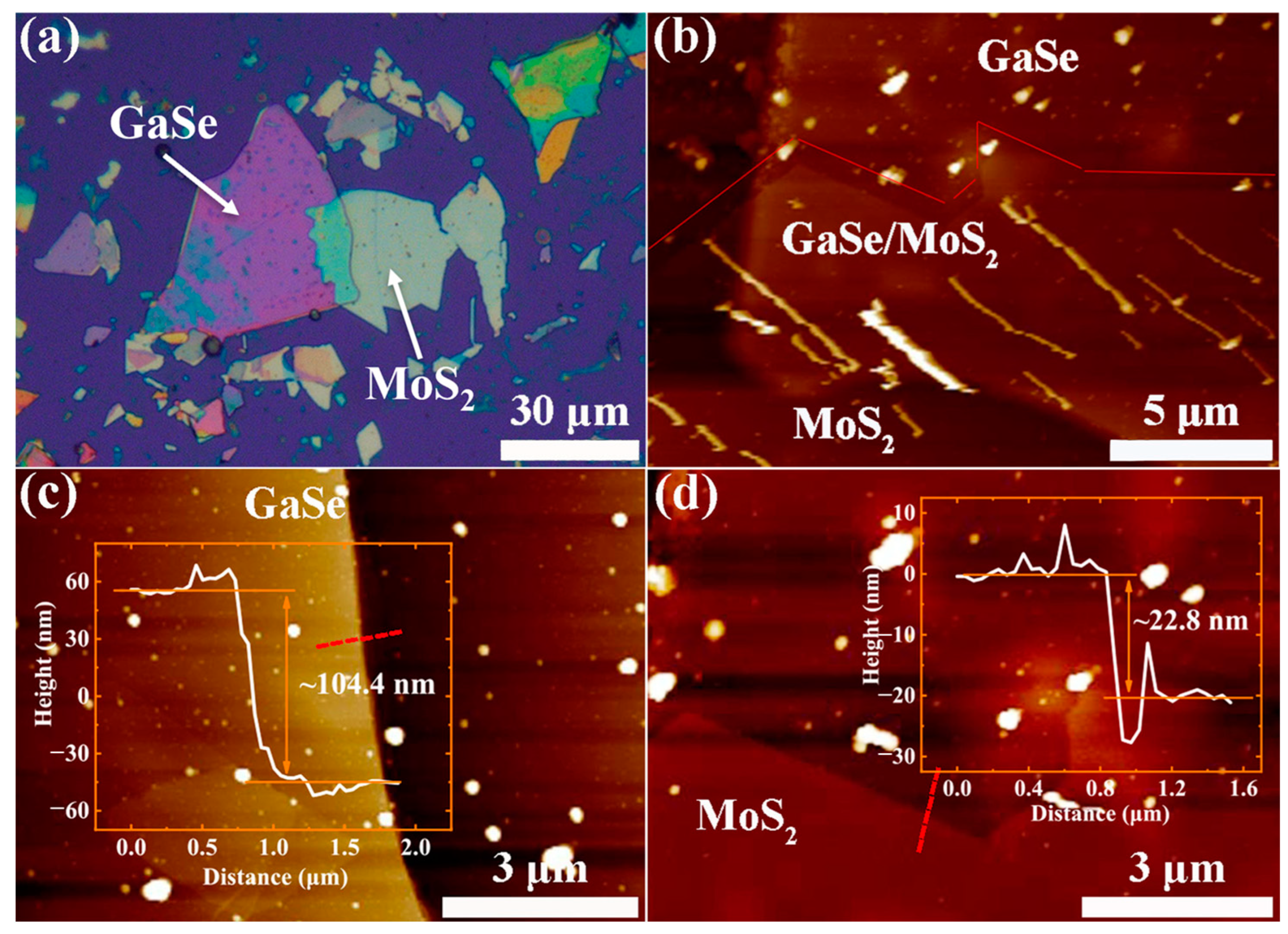
3.1. Characterization of Individual GaSe, MoS2 and Their Heterostructure

The optical microscopy (OM) image of the vertically stacked GaSe/MoS2 vdW heterojunction on the SiO2/Si substrate is depicted in Figure 1a. Clear optical contrast shows GaSe on the left and MoS2 on the right, which are marked by the arrows, respectively. Note that the sample shows a clean surface and sharp interface. The atomic force microscopy (AFM) images of GaSe/MoS2, GaSe and MoS2 samples are correspondingly displayed in Figure 1b–d. The portion above the red line in Figure 1b is GaSe, the portion on the lower left is MoS2, and the middle part is the GaSe/MoS2 vdW heterostructure. In Figure 1c,d, the corresponding height profiles in the insets reveal that the thicknesses of the GaSe and MoS2 nanosheets are ~104.4 nm and ~22.8 nm, respectively. For more information of the transmission electron microscope (TEM), high-resolution transmission electron microscopy (HRTEM) and the corresponding energy dispersive spectrometer (EDS) mapping images of the GaSe/MoS2 vdW heterojunction, please refer to Figure S1.
In order to characterize the optical property of the GaSe/MoS2 vdW heterojunction on SiO2/Si, the Raman and PL spectra of GaSe, MoS2 and their overlapped area (GaSe/MoS2 heterojunction) were measured and the spectra are presented in Figure 2a and Figure 2b, respectively. In Raman spectra, GaSe features three primary peaks at 134 cm−1 (A11g), 212 cm−1 (E12g) and 308 cm−1 (A21g), respectively, verifying the excellent crystal quality of the GaSe nanosheet [37]. Among them, A11g and A21g are associated with the out-of-plane vibration mode, whereas E12g derives from the in-plane vibration mode [38]. The two typical Raman peaks of MoS2 are positioned at 383 cm−1 (E12g) and 408 cm−1 (A1g), which associates with the in-plane vibration mode and the out-of-plane vibration mode, respectively [39]. In the overlapped area where GaSe and MoS2 overlap, all characteristic Raman peaks of both GaSe and MoS2 are visible, demonstrating the construction of the heterojunction.
At an ambient temperature, the PL spectra of GaSe reveals a strong and narrow peak at approximately 2.00 eV, indicating that the nanosheet is ε-GaSe [40]. A weak and wide PL peak of MoS2 is detected at approximately 1.84 eV at room temperature, which corresponds to direct excitonic transition. Both Raman and PL spectra demonstrate that the GaSe and MoS2 nanosheets have excellent crystallinity. In the overlapping area, all characteristic PL peaks of both GaSe and MoS2 are likewise depicted, demonstrating the construction of a vertical GaSe/MoS2 vdW heterojunction. The decrease in PL intensity observed at the heterojunction suggests that a portion of the photoexcited charge carriers undergo nonradiative recombination instead of contributing to PL emission. This phenomenon is indicative of ultrafast photoexcited carrier transport at the interface of the heterostructure, providing evidence that the GaSe/MoS2 vdW heterojunction exhibits a type-II band alignment.
The schematic diagrams of crystal structures and energy bands for MoS2 and GaSe are illustrated in Figure S2 [28,41]. The vertically stacked GaSe/MoS2 vdW heterostructure generates a type-II band alignment, with the minimum conduction band corresponding to MoS2 and the maximum valence band corresponding to GaSe. This heterostructure results in separating electrons and holes residing in two separated layers upon optical excitation [16], which is advantageous for the fabrication of high-performance photodetectors.

3.2. Fabrication Process of Photodetectors

A flexible photodetector based on a vertically stacked GaSe/MoS2 vdW heterojunction was fabricated and the flow chart for the preparation process is showcased in Figure 3a. In order to present the transfer procedure, the OM and AFM images of GaSe and MoS2 are exhibited in Figure S3. The thickness of the GaSe nanosheet and MoS2 nanosheet is ~24.7 nm and ~170 nm, respectively. Both the GaSe and MoS2 work together as the light absorbing layer of the photodetector. They form the type-II heterostructure, which can effectively separate the photogenerated carriers. In addition, MoS2 is extraordinarily stable in air, while GaSe is not as stable as MoS2. Therefore, MoS2 on the upper layer can also act as a protective layer for the device. The photograph of the flexible photodetector fabricated by the vertically stacked GaSe/MoS2 vdW heterostructure is presented in Figure 3b, and Figure 3c is the OM image of the device. Note that the photoelectric properties of photodetectors based on the individual GaSe, MoS2 and GaSe/MoS2 heterojunction were determined by connecting different combination of Au electrodes pairs of 1&2, 3&4 and 1&4, respectively. Therefore, we are capable of realizing the contrastive measurement of different photodetectors by an in situ experimental manner directly. The effective area of the GaSe, MoS2 and GaSe/MoS2 vdW heterojunction photodetectors were measured to be 202, 43 and 137 μm2, respectively.

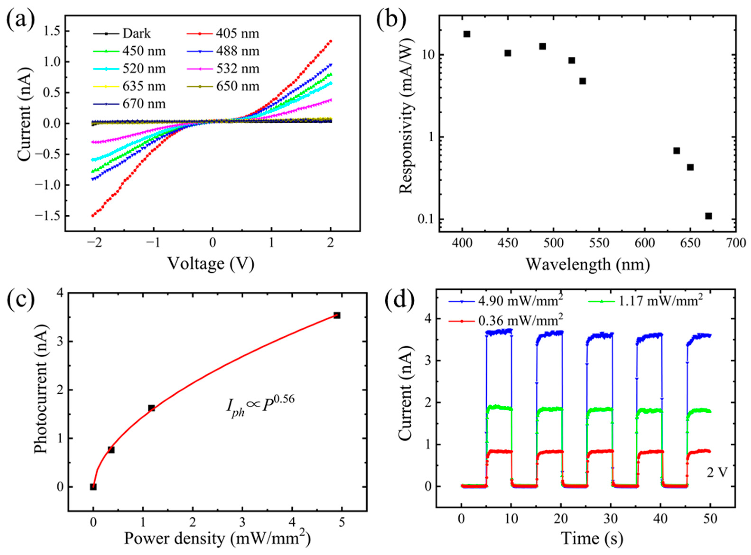
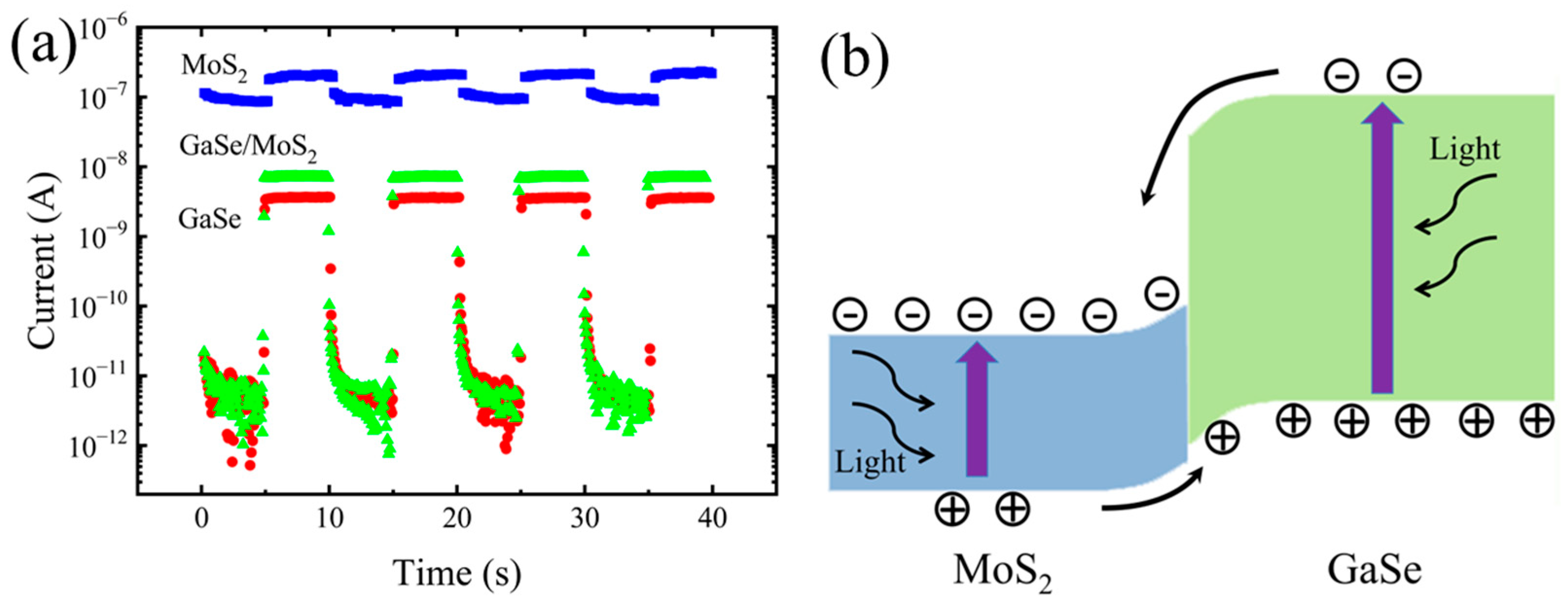
3.3. Photoresponse of the GaSe, MoS2 and Heterostructure Photodetector

To figure out the photoelectric performance of the GaSe photodetector, systematic measurements were performed. The current–voltage (I-V) curves in the dark and under the incident light of varying wavelengths are presented in Figure 4a. These I-V curves are generally symmetrical around the origin, suggesting that the contacts between the GaSe and two Au electrodes are nearly consistent. At a bias of 2 V, the dark current (Idark) of the photodetector is as low as 31 pA. The responses of the device to the lights with wavelengths of 670 nm, 650 nm and 635 nm are quite weak. However, when the incident photon energy is greater than the energy gap of GaSe, the responses of the device to the incident lights become apparent, with the response to 405 nm light the most evident. The spectral responsivity of the device at 2 V shown in Figure 4b further proves this result. Under the illumination with the wavelength of 450 nm and the light power density of 0.36 mW/mm2, the responsivity and the detectivity of the GaSe photodetector are 10.5 mA/W and 4.74 × 10⁷ Jones. Figure S4a also depicts the I-V curves of the GaSe photodetector under varying light power densities and the currents under incident light (Ilight) increase with the increasing light power densities. Figure 4c depicts the relationship between the photocurrent I (I = Ilight Idark) of the device and the incident light power density P with 450 nm incident light at 2 V. The curve was fitted with IPα, where α is a constant evincing the capability of the photocurrent response to the light power density and its value is fitted to be 0.56. The nonlinear index 0 < α < 1 often appears in semiconductor photodetectors, which is associated with the intricate process of electron–hole generation, trapping and recombination inside the semiconductor [42]. The power law fitting can more intuitively reflect the change of the photocurrent with optical power density. Photogenerated electrons are captured by the trap states. As the incident light intensity rises, the existing trap states become saturated, and subsequently, newly generated electron–hole pairs do not significantly contribute to the charge transfer process. This is due to the swift recombination of electrons and holes, limiting their effective participation in the overall charge transfer dynamics [43]. If the trap states are rare, the photocurrent will be proportional to the light power density linearly and α is close to 1 [44]. Here, α is much smaller than 1, which implies there are some trap states in GaSe. Figure 4d illustrates the temporal photoresponse of the photodetector at 2 V while switching 450 nm light with light power densities of 0.36, 1.17 and 4.90 mW/mm2. The device is capable of reliably and consistently detecting light. As the light power density increases, the ratio of the current under incident light Ilight to dark current Idark rises, which is 225, 460 and 925, successively. The maximum value of Ilight of GaSe merely reaches 3.7 nA. The single-cycle switching characteristic curve of the GaSe photodetector at 2 V is shown in Figure S4b. Both the response time and the recovery time of the device are 40 ms. In general, the GaSe photodetector shows relatively limited photoelectric performances in terms of the responsivity of devices, yet it presents superiority in detecting light consistently with an exceptional response speed.
The photoelectric performances of the MoS2 photodetector were also measured. The I-V curves in the dark and under incident light of various wavelengths are evidenced in Figure 5a. These I-V curves are likewise nearly symmetric around the origin, indicating that the contacts between MoS2 and two Au electrodes are essentially consistent. At a bias of 2 V, the dark current of the photodetector reaches 72.7 nA. Owing to the intrinsic long-wavelength restriction of MoS2 being 1033 nm, the responses of the device to visible light are thoroughly evident. The spectral responsivity of the device at 2 V, as seen in Figure 5b, further substantiates this assertion. Under the illumination of light with the wavelength of 450 nm and the light power density of 0.36 mW/mm2, the responsivity and the detectivity of the photodetector are fairly high, attaining 2496.8 mA/W and 1.07 × 10⁸ Jones. In addition, the I-V curves of the MoS2 photodetector under the illumination of light with various light power densities are illustrated in Figure S5a and Ilight increases with the increasing light power densities. Figure 5c plots the relationship between the device photocurrent I and incident light power density P with 450 nm incident light at 2 V. The curve is similarly fitted with IPα, and the value of α is 0.43, denoting that MoS2 includes certain trap states [42,43,44]. Figure 5d portrays the photoresponse of the photodetector at 2 V, switching the 450 nm light with 0.36, 1.17 and 4.90 mW/mm2 light power densities. The device can also detect light consistently and reliably. Due to the significant dark current, the ratio of Ilight to Idark is relatively low, with a maximum value of merely 2.3. However, the maximum Ilight of MoS2 is 236 nA, which is a relatively high value. Figure S5b depicts the single-cycle switching characteristic curve of the MoS2 photodetector under 450 nm light illumination with 4.90 mW/mm2 light power density. Both the response time and the recovery time of the device are 40 ms. In summary, the ratio of Ilight to Idark of the MoS2 photodetector are barely satisfactory. Nonetheless, it realizes the detection of light consistently, and its responsivity is remarkably high with an outstanding response speed.
To compare the photoelectric performances, the photodetector fabricated by the GaSe/MoS2 vdW heterojunction is measured as well. The I-V curves of the GaSe/MoS2 photodetector in the dark and under incident light with various wavelengths are shown in Figure 6a. These I-V curves closely resemble those of the GaSe photodetector. Similar to the GaSe photodetector, the dark current value of the GaSe/MoS2 photodetector is only 30 pA at 2 V. They differ in that the GaSe/MoS2 photodetector exhibits a relatively pronounced rectification effect. The spectral responsivity of the device at 2 V, as seen in Figure 6b, is comparable to that of individual GaSe photodetectors. Under the illumination of light with the wavelength of 450 nm and the light power density of 0.36 mW/mm2, however, the responsivity and the detectivity of the GaSe/MoS2 photodetector are greater, reaching 22.6 mA/W and 8.54 × 10⁷ Jones. Moreover, the I-V curves of the GaSe/MoS2 vdW photodetector with varying light power densities are presented in Figure S6a and the currents under incident light show an increase trend with the increasing light power densities. Photocurrent as a function of light power density at 2 V is depicted in Figure 6c. The curve is also fitted with IPα, and the value of α is 0.60, which is consistent with the previous findings. The temporal response of the GaSe/MoS2 photodetector at 2 V while switching 450 nm light with 0.36, 1.17 and 4.90 mW/mm2 light power densities is presented in Figure 6d. The device can also realize reliably and consistently the detection of light. As a result of the strong suppression of the dark current, the ratio of Ilight to Idark is rather high. As the light power density grows, so does the ratio, which is successively 380, 1180 and 2360, respectively. The highest value of Ilight reaches 7.5 nA. The single-cycle switching characteristic curve of the GaSe/MoS2 vdW photodetector is displayed in Figure S6b. Both the response and recovery time of the device are about 20 ms, which are similar with that of the GaSe photodetector and the MoS2 photodetector.
The comparative performance of the individual GaSe, MoS2 and GaSe/MoS2 vdW heterojunction photodetectors is shown in Figure 7a. Note that the comparison of photoelectric properties is also presented in Table S1. In conclusion, GaSe, MoS2 and GaSe/MoS2 photodetectors can all detect light in a repeatable and stable manner, and their response rates are all expeditious. The heterostructure photodetector exhibits higher responsivity and detectivity than the GaSe photodetector but lower responsivity and detectivity than the MoS2 photodetector. Furthermore, The heterostructure device has the largest ratio of Ilight to Idark among all the devices. The GaSe/MoS2 vdW heterojunction photodetector features the combined benefits of both GaSe and MoS2. The aforementioned results demonstrate unequivocally that type-II vdW heterostructures significantly improve the performances of photodetectors. We have also provided the comparison of the photoelectric performances of the GaSe/MoS2 heterostructure, individual MoS2 and GaSe devices in this paper with those in other related literatures, and they are listed in Table S2 [18,19,25,27,29,30,45]. The photodetectors in this work show comparable performances with those in the previous reported papers. Note that the photodetectors in this work are fabricated on the flexible PET substrates rather than rigid substrates. Therefore, our photodetectors show more superiority in the flexible situation compared with other ones.
The rationale for the performance enhancement may be deduced from the band alignment diagram of the GaSe/MoS2 heterostructure, which is presented in Figure 7b. The energy bands of the two materials intersect, and the heterostructure shows a type-II alignment. The type-II band alignment is responsible for the enhanced performance of the heterostructure photodetector. Due to the different Fermi levels of MoS2 and GaSe, electron carriers tend to flow into GaSe, whereas hole carriers tend to flow into MoS2. An intrinsic electric field is produced at the interface of MoS2 and GaSe, causing the energy levels to bend near the surfaces of MoS2 and GaSe. At the interface of MoS2 and GaSe, a stable built-in electric field is created when the Fermi levels of MoS2 and GaSe are eventually equal. In the meantime, the built-in electric field causes the photogenerated electrons and holes to drift in opposing directions under illumination, which effectively separates two types of carriers, prolongs the life of photogenerated carriers, improves the photoconductive gain of the device and eventually enhances the performance of the photodetector. When the GaSe/MoS2 heterojunction is under the dark environment, the carriers are mainly generated thermally and driven by the electric field. When the GaSe/MoS2 heterojunction is in the light environment, the light triggers the production of carriers. The energy of the photons excites electrons to jump from the valence band to the conduction band, generating more electron–hole pairs and resulting in an enhanced photocurrent.

3.4. Flexible GaSe/MoS2 Heterojunction Photodetector

The flexible GaSe/MoS2 vdW heterojunction photodetector is bendable and it is able to work effectively in a bent state. Figure 8a illustrates a schematic diagram of the bent heterojunction device (top) and a photograph of the device with a 1.5 cm radius of curvature (bottom). The temporal photoresponse of the device in the straight state and in the bent state at 2 V with switching the 450 nm light are shown in Figure 8b. The dark current of both states is nearly equal, while the Ilight of the device shows a minor decreasing trend at the bent state, which may cause a decrease of the on–off ratio slightly. In the interim of switching measurements, the photodetector maintains a repeatable and reliable photodetection capacity, showcasing its superior flexible adaptability at the bent state. The demonstration for the long-term stability of the flexible GaSe/MoS2 vdW heterojunction photodetector was also performed. Please refer to Figure S7 for more information.

4. Conclusions

In this work, the type-II band alignment of the vertically stacked GaSe/MoS2 vdW heterojunction was verified. Subsequently, we achieved the successful fabrication of a flexible photodetector based on the GaSe/MoS2 heterojunction on a PET substrate. Photoelectric properties of individual GaSe, MoS2 and GaSe/MoS2 heterojunction photodetectors were characterized in situ by connecting various combinations of Au electrode pairs. All variations of photodetectors realized the detection of light consistently and reliably, exhibiting relatively remarkable responsivities on the flexible substrate with rapid response speed. Notably, the heterojunction photodetector achieves the highest on–off ratio of 2360 with the light wavelength of 450 nm and the light power density of 4.90 mW/mm2. The boost of photoelectric performance for the heterostructure photodetector is attributed to the formation of type-II band alignment. Furthermore, the exceptional flexible adaptability of the photodetector based on the GaSe/MoS2 heterojunction is particularly impressive. This study directly and experimentally showcases the efficacy of the type-II vdW heterojunction for advancing flexible photodetectors.

Supplementary Materials

The following are available online at https://www.mdpi.com/article/10.3390/cryst13111602/s1, Figure S1: Structure and energy spectrum characterization of the GaSe/MoS2 van der Waals heterojunction, Figure S2: Crystal structures and energy-band diagrams of MoS2 and GaSe [28,41], Figure S3: Fabrication process of GaSe/MoS2 photodetector, Figure S4: Photoresponse of the GaSe photodetector, Figure S5: Photoresponse of the MoS2 photodetector, Figure S6: Photoresponse of the GaSe/MoS2 vdW heterojunction photodetector, Figure S7: Stability of the GaSe/MoS2 photodetector, Table S1: Comparison of photoelectric properties for individual GaSe, MoS2 and GaSe/MoS2 vdW heterostructures, Table S2: Comparison of photoelectric performances with those in other related literatures [18,19,25,27,29,30,45].

Author Contributions

Conceptualization, Y.L.; data curation, X.T., Z.W. and Y.L.; formal analysis, S.W. (Shuai Wang), X.T. and Z.W.; funding acquisition, Z.W., S.W. (Sumei Wu), Y.W. (Yingying Wang) and Z.Z.; investigation, S.W. (Shuai Wang), E.A., X.S. and H.T.; methodology, S.W. (Shuai Wang) and Z.W.; project administration, Z.Z.; resources, Y.W. (Yang Wen), S.W. (Sumei Wu), Y.C., Y.W. (Yingying Wang) and Z.Z.; writing—original draft, X.T.; writing—review and editing, Z.W. and Y.L. All authors have read and agreed to the published version of the manuscript.

Funding

This research was funded by the National Natural Science Foundation of China, grant number 52171229 and 12204084; Liaoning Province Applied Basic Research Program, grant number 2023JH2/101600045; Liaoning Province Education Department Basic Scientific Research Project, grant number LJKQZ20222301; Liaoning Education Department Scientific Research Fund Project, grant number JDL2020012; Dalian Science and Technology Innovation Fund, grant number 2022RQ025; Shandong Provincial Natural Science Foundation, grant number ZR2020MF122.

Data Availability Statement

The data presented in this study are available on request from the corresponding author.

Conflicts of Interest

The authors declare no conflict of interest.

References

  1. Liu, J.; Hu, D.; Ni, M.; Zou, Y.; Gu, Y.; Han, Z.; Li, J.; He, Y.; Zhang, Z.; Xu, X. Monolithic RGB-NIR Perovskite Photodetector for Fused Multispectral Sensing and Imaging. J. Phys. Chem. Lett. 2022, 13, 3659–3666. [Google Scholar] [CrossRef] [PubMed]
  2. Liu, Y.; Liu, C.; Shen, K.; Sun, P.; Li, W.; Zhao, C.; Ji, Z.; Mai, Y.; Mai, W. Underwater Multispectral Computational Imaging Based on a Broadband Water-Resistant Sb2Se3 Heterojunction Photodetector. ACS Nano 2022, 16, 5820–5829. [Google Scholar] [CrossRef]
  3. Wu, W.; Zhou, M.; Li, D.; Li, S.; Yang, Z.; Huo, Z.; Wu, Y.; Tan, Y.; Han, X.; Pan, C.; et al. A novel visible light sensing and recording system enabled by integration of photodetector and electrochromic devices. Nanoscale 2021, 13, 9177–9184. [Google Scholar] [CrossRef]
  4. Wu, W.; Han, X.; Li, J.; Wang, X.; Zhang, Y.; Huo, Z.; Chen, Q.; Sun, X.; Xu, Z.; Tan, Y.; et al. Ultrathin and Conformable Lead Halide Perovskite Photodetector Arrays for Potential Application in Retina-Like Vision Sensing. Adv. Mater. 2021, 33, 2006006. [Google Scholar] [CrossRef] [PubMed]
  5. Zhang, J.; Jiang, M.; Bian, L.; Wu, D.; Qin, H.; Yang, W.; Zhao, Y.; Wu, Y.; Zhou, M.; Lu, S. A Self-Powered Transparent Photodetector Based on Detached Vertical (In,Ga)N Nanowires with 360 degrees Omnidirectional Detection for Underwater Wireless Optical Communication. Nanomaterials 2021, 11, 2959. [Google Scholar] [CrossRef] [PubMed]
  6. Lu, Y.; Wang, Y.; Xu, C.; Xie, C.; Li, W.; Ding, J.; Zhou, W.; Qin, Z.; Shen, X.; Luo, L.B. Construction of PtSe2/Ge heterostructure-based short-wavelength infrared photodetector array for image sensing and optical communication applications. Nanoscale 2021, 13, 7606–7612. [Google Scholar] [CrossRef]
  7. Liu, S.; Zhang, X.D.; Gu, X.; Ming, D. Photodetectors based on two dimensional materials for biomedical application. Biosens. Bioelectron. 2019, 143, 111617. [Google Scholar] [CrossRef]
  8. Xin, Y.; Wang, X.; Chen, Z.; Weller, D.; Wang, Y.; Shi, L.; Ma, X.; Ding, C.; Li, W.; Guo, S.; et al. Polarization-Sensitive Self-Powered Type-II GeSe/MoS2 van der Waals Heterojunction Photodetector. ACS Appl. Mater. Interfaces 2020, 12, 15406–15413. [Google Scholar] [CrossRef]
  9. Varghese, A.; Saha, D.; Thakar, K.; Jindal, V.; Ghosh, S.; Medhekar, N.V.; Ghosh, S.; Lodha, S. Near-Direct Bandgap WSe2/ReS2 Type-II pn Heterojunction for Enhanced Ultrafast Photodetection and High-Performance Photovoltaics. Nano Lett. 2020, 20, 1707–1717. [Google Scholar] [CrossRef]
  10. Jia, C.; Huang, X.; Wu, D.; Tian, Y.; Guo, J.; Zhao, Z.; Shi, Z.; Tian, Y.; Jie, J.; Li, X. Ultrasensitive self-driven broadband photodetector based on a 2D-WS2/GaAs type-II Zener heterojunction. Nanoscale 2020, 12, 4435–4444. [Google Scholar] [CrossRef]
  11. Duan, J.; Chava, P.; Ghorbani-Asl, M.; Lu, Y.; Erb, D.; Hu, L.; Echresh, A.; Rebohle, L.; Erbe, A.; Krasheninnikov, A.V.; et al. Self-Driven Broadband Photodetectors Based on MoSe2/FePS3 van der Waals n-p Type-II Heterostructures. ACS Appl. Mater. Interfaces 2022, 14, 11927–11936. [Google Scholar] [CrossRef]
  12. Wang, H.; Li, Z.; Li, D.; Chen, P.; Pi, L.; Zhou, X.; Zhai, T. Van der Waals Integration Based on Two-Dimensional Materials for High-Performance Infrared Photodetectors. Adv. Funct. Mater. 2021, 31, 2103106. [Google Scholar] [CrossRef]
  13. Tan, C.; Cao, X.; Wu, X.J.; He, Q.; Yang, J.; Zhang, X.; Chen, J.; Zhao, W.; Han, S.; Nam, G.H.; et al. Recent Advances in Ultrathin Two-Dimensional Nanomaterials. Chem. Rev. 2017, 117, 6225–6331. [Google Scholar] [CrossRef] [PubMed]
  14. Long, R.; Prezhdo, O.V. Quantum Coherence Facilitates Efficient Charge Separation at a MoS2/MoSe2 van der Waals Junction. Nano Lett. 2016, 16, 1996–2003. [Google Scholar] [CrossRef] [PubMed]
  15. Pasupuleti, K.S.; Reddeppa, M.; Park, B.-G.; Oh, J.-E.; Kim, S.-G.; Kim, M.-D. Efficient Charge Separation in Polypyrrole/GaN-Nanorod-Based Hybrid Heterojunctions for High-Performance Self-Powered UV Photodetection. Phys. Status Solidi (RRL) Rapid Res. Lett. 2021, 15, 2000518. [Google Scholar] [CrossRef]
  16. Hong, X.; Kim, J.; Shi, S.F.; Zhang, Y.; Jin, C.; Sun, Y.; Tongay, S.; Wu, J.; Zhang, Y.; Wang, F. Ultrafast charge transfer in atomically thin MoS2/WS2 heterostructures. Nat. Nanotechnol. 2014, 9, 682–686. [Google Scholar] [CrossRef]
  17. Rybkovskiy, D.V.; Arutyunyan, N.R.; Orekhov, A.S.; Gromchenko, I.A.; Vorobiev, I.V.; Osadchy, A.V.; Salaev, E.Y.; Baykara, T.K.; Allakhverdiev, K.R.; Obraztsova, E.D. Size-induced effects in gallium selenide electronic structure: The influence of interlayer interactions. Phys. Rev. B 2011, 84, 085314. [Google Scholar] [CrossRef]
  18. Hu, P.; Wen, Z.; Wang, L.; Tan, P.; Xiao, K. Synthesis of Few-Layer GaSe Nanosheets for High Performance Photodetectors. ACS Nano 2012, 6, 5988–5994. [Google Scholar] [CrossRef]
  19. Huang, H.; Wang, P.; Gao, Y.; Wang, X.; Lin, T.; Wang, J.; Liao, L.; Sun, J.; Meng, X.; Huang, Z.; et al. Highly sensitive phototransistor based on GaSe nanosheets. Appl. Phys. Lett. 2015, 107, 143112. [Google Scholar] [CrossRef]
  20. Allakhverdiev, K.R.; Yetis, M.Ö.; Özbek, S.; Baykara, T.K.; Salaev, E.Y. Effective nonlinear GaSe crystal. Optical properties and applications. Laser Phys. 2009, 19, 1092–1104. [Google Scholar] [CrossRef]
  21. Tang, Y.; Xie, W.; Mandal, K.C.; McGuire, J.A.; Lai, C.W. Optical and spin polarization dynamics in GaSe nanoslabs. Phys. Rev. B 2015, 91, 195429. [Google Scholar] [CrossRef]
  22. Kuc, A.; Zibouche, N.; Heine, T. Influence of quantum confinement on the electronic structure of the transition metal sulfide TS2. Phys. Rev. B 2011, 83, 245213. [Google Scholar] [CrossRef]
  23. Radisavljevic, B.; Radenovic, A.; Brivio, J.; Giacometti, V.; Kis, A. Single-layer MoS2 transistors. Nat. Nanotechnol. 2011, 6, 147–150. [Google Scholar] [CrossRef] [PubMed]
  24. Chen, H.; Wen, X.; Zhang, J.; Wu, T.; Gong, Y.; Zhang, X.; Yuan, J.; Yi, C.; Lou, J.; Ajayan, P.M.; et al. Ultrafast formation of interlayer hot excitons in atomically thin MoS2/WS2 heterostructures. Nat. Commun. 2016, 7, 12512. [Google Scholar] [CrossRef] [PubMed]
  25. Tang, W.; Liu, C.; Wang, L.; Chen, X.; Luo, M.; Guo, W.; Wang, S.-W.; Lu, W. MoS2 nanosheet photodetectors with ultrafast response. Appl. Phys. Lett. 2017, 111, 153502. [Google Scholar] [CrossRef]
  26. Xie, Y.; Zhang, B.; Wang, S.; Wang, D.; Wang, A.; Wang, Z.; Yu, H.; Zhang, H.; Chen, Y.; Zhao, M.; et al. Ultrabroadband MoS2 Photodetector with Spectral Response from 445 to 2717 nm. Adv. Mater. 2017, 29, 1605972. [Google Scholar] [CrossRef]
  27. Zhou, N.; Wang, R.; Zhou, X.; Song, H.; Xiong, X.; Ding, Y.; Lu, J.; Gan, L.; Zhai, T. P-GaSe/N-MoS2 Vertical Heterostructures Synthesized by van der Waals Epitaxy for Photoresponse Modulation. Small 2018, 14, 1702731. [Google Scholar] [CrossRef]
  28. Islam, A.; Lee, J.; Feng, P.X.-L. Atomic Layer GaSe/MoS2 van der Waals Heterostructure Photodiodes with Low Noise and Large Dynamic Range. ACS Photonics 2018, 5, 2693–2700. [Google Scholar] [CrossRef]
  29. He, Z.; Guo, J.; Li, S.; Lei, Z.; Lin, L.; Ke, Y.; Jie, W.; Gong, T.; Lin, Y.; Cheng, T.; et al. GaSe/MoS2 Heterostructure with Ohmic-Contact Electrodes for Fast, Broadband Photoresponse, and Self-Driven Photodetectors. Adv. Mater. Interfaces 2020, 7, 1901848. [Google Scholar] [CrossRef]
  30. Zou, Z.; Liang, J.; Zhang, X.; Ma, C.; Xu, P.; Yang, X.; Zeng, Z.; Sun, X.; Zhu, C.; Liang, D.; et al. Liquid-Metal-Assisted Growth of Vertical GaSe/MoS2 p-n Heterojunctions for Sensitive Self-Driven Photodetectors. ACS Nano 2021, 15, 10039–10047. [Google Scholar] [CrossRef]
  31. Wu, X.; Guo, W.; Li, M.; Xiao, C.; Ou, T.; Qiu, Z.; Wang, Y. Influence of the Device Structure on the Electrical and Photodetector Properties of n-MoS2/p-GaSe Heterojunction Optoelectronic Devices. ACS Appl. Nano Mater. 2023, 6, 11327–11333. [Google Scholar] [CrossRef]
  32. Dong, T.; Simões, J.; Yang, Z. Flexible Photodetector Based on 2D Materials: Processing, Architectures, and Applications. Adv. Mater. Interfaces 2020, 7, 1901657. [Google Scholar] [CrossRef]
  33. Choi, J.M.; Jang, H.Y.; Kim, A.R.; Kwon, J.D.; Cho, B.; Park, M.H.; Kim, Y. Ultra-flexible and rollable 2D-MoS2/Si heterojunction-based near-infrared photodetector via direct synthesis. Nanoscale 2021, 13, 672–680. [Google Scholar] [CrossRef] [PubMed]
  34. Luo, S.; Wu, Z.; Zhao, J.; Luo, Z.; Qiu, Q.; Li, Z.; Wu, H.; Xing, G.; Wu, C. ZIF-67 Derivative Decorated MXene for a Highly Integrated Flexible Self-Powered Photodetector. ACS Appl. Mater. Interfaces 2022, 14, 19725–19735. [Google Scholar] [CrossRef]
  35. Kim, T.; Jeong, S.; Kim, K.H.; Shim, H.; Kim, D.; Kim, H.J. Engineered Surface Halide Defects by Two-Dimensional Perovskite Passivation for Deformable Intelligent Photodetectors. ACS Appl. Mater. Interfaces 2022, 14, 26004–26013. [Google Scholar] [CrossRef]
  36. Xue, Y.; Zhang, Y.; Liu, Y.; Liu, H.; Song, J.; Sophia, J.; Liu, J.; Xu, Z.; Xu, Q.; Wang, Z.; et al. Scalable Production of a Few-Layer MoS2/WS2 Vertical Heterojunction Array and Its Application for Photodetectors. ACS Nano 2016, 10, 573–580. [Google Scholar] [CrossRef]
  37. Wu, Y.; Fuh, H.-R.; Zhang, D.; Coileáin, C.Ó.; Xu, H.; Cho, J.; Choi, M.; Chun, B.S.; Jiang, X.; Abid, M.; et al. Simultaneous large continuous band gap tunability and photoluminescence enhancement in GaSe nanosheets via elastic strain engineering. Nano Energy 2017, 32, 157–164. [Google Scholar] [CrossRef]
  38. Rahaman, M.; Bejani, M.; Salvan, G.; Lopez-Rivera, S.A.; Pulci, O.; Bechstedt, F.; Zahn, D.R.T. Vibrational properties of GaSe: A layer dependent study from experiments to theory. Semicond. Sci. Tech. 2018, 33, 125008. [Google Scholar] [CrossRef]
  39. Li, H.; Zhang, Q.; Yap, C.C.R.; Tay, B.K.; Edwin, T.H.T.; Olivier, A.; Baillargeat, D. From Bulk to Monolayer MoS2: Evolution of Raman Scattering. Adv. Funct. Mater. 2012, 22, 1385–1390. [Google Scholar] [CrossRef]
  40. Jie, W.; Chen, X.; Li, D.; Xie, L.; Hui, Y.Y.; Lau, S.P.; Cui, X.; Hao, J. Layer-dependent nonlinear optical properties and stability of non-centrosymmetric modification in few-layer GaSe sheets. Angew. Chem. Int. Ed. 2015, 54, 1185–1189. [Google Scholar] [CrossRef]
  41. Kwak, J.Y.; Hwang, J.; Calderon, B.; Alsalman, H.; Munoz, N.; Schutter, B.; Spencer, M.G. Electrical Characteristics of Multilayer MoS2 FET’s with MoS2/Graphene Heterojunction Contacts. Nano Lett. 2014, 14, 4511–4516. [Google Scholar] [CrossRef] [PubMed]
  42. Kind, H.; Yan, H.; Messer, B.; Law, M.; Yang, P. Nanowire Ultraviolet Photodetectors and Optical Switches. Adv. Mater. 2002, 14, 158–160. [Google Scholar] [CrossRef]
  43. Shao, D.; Gao, J.; Chow, P.; Sun, H.; Xin, G.; Sharma, P.; Lian, J.; Koratkar, N.A.; Sawyer, S. Organic–Inorganic Heterointerfaces for Ultrasensitive Detection of Ultraviolet Light. Nano Lett. 2015, 15, 3787–3792. [Google Scholar] [CrossRef] [PubMed]
  44. Xing, X.; Zhang, Q.; Huang, Z.; Lu, Z.; Zhang, J.; Li, H.; Zeng, H.; Zhai, T. Strain Driven Spectral Broadening of Pb Ion Exchanged CdS Nanowires. Small 2016, 12, 874–881. [Google Scholar] [CrossRef] [PubMed]
  45. Yin, Z.; Li, H.; Li, H.; Jiang, L.; Shi, Y.; Sun, Y.; Lu, G.; Zhang, Q.; Chen, X.; Zhang, H. Single-Layer MoS2 Phototransistors. ACS Nano 2011, 6, 74–80. [Google Scholar] [CrossRef]
Figure 1. Morphology characterization of GaSe, MoS2 and the heterojunction. (a) OM image of the vertically stacked GaSe/MoS2 vdW heterojunction on the SiO2/Si substrate. (bd) AFM images of GaSe/MoS2, GaSe and MoS2 regions, respectively. Height profiles in the insets of (c) and (d) show the thicknesses of GaSe and MoS2. The red dotted lines show the locations for the measurement of height profiles.
Crystals 13 01602 g001
Figure 2. Raman and PL spectra of individual GaSe, MoS2 and their heterostructure. (a) Raman spectra and (b) PL spectra collected from GaSe, MoS2 and their overlapped region (GaSe/MoS2 vdW heterojunction), respectively.
Crystals 13 01602 g002
Figure 3. Fabrication process and photograph of photodetectors. (a) Brief flow chart of the fabrication of flexible photodetectors based on vertically stacked GaSe/MoS2 vdW heterojunction. (b) Photograph of the device illustrating its flexibility. (c) OM image of the device with different combinations of Au electrodes pairs.
Crystals 13 01602 g003
Figure 4. Photoresponse of the GaSe photodetector. (a) I-V curves in the dark and under incident light with different wavelengths. (b) Spectral responsivity of the photodetector at 2 V. (c) The relationship between device photocurrent and incident light power density. (d) Temporal photoresponse of the device by switching 450 nm light with different light power densities.
Crystals 13 01602 g004
Figure 5. Photoresponse of the MoS2 photodetector. (a) I-V curves in the dark and under incident light with different wavelengths. (b) Spectral responsivity of the photodetector at 2 V. (c) Photocurrent versus light power density at 2 V. (d) Temporal photoresponse of the device at 2 V by switching 450 nm light with different light power densities.
Crystals 13 01602 g005
Figure 6. Photoresponse of the GaSe/MoS2 vdW heterojunction photodetector. (a) I-V curves in the dark and under incident light with different wavelengths. (b) Spectral responsivity of the photodetector at 2 V. (c) Photocurrent versus light power density at 2 V. (d) Temporal photoresponse of the device at 2 V by switching 450 nm light with different light power densities.
Crystals 13 01602 g006
Figure 7. Comparison of performance for the photodetectors and band alignment of the heterojunction. (a) Performance comparison of the GaSe, MoS2 and GaSe/MoS2 vdW heterojunction photodetectors. (b) Band alignment at the interface of the GaSe/MoS2 heterojunction.
Crystals 13 01602 g007
Figure 8. Measurement of the flexible GaSe/MoS2 heterojunction photodetector. (a) Schematic diagram (top) and photograph (bottom) of the vertically stacked type-II GaSe/MoS2 vdW heterojunction photodetector at a bent state. (b) Temporal photoresponse of the heterojunction device at a bias of 2 V by switching 450 nm light without bending and at the bent state.
Crystals 13 01602 g008
Disclaimer/Publisher’s Note: The statements, opinions and data contained in all publications are solely those of the individual author(s) and contributor(s) and not of MDPI and/or the editor(s). MDPI and/or the editor(s) disclaim responsibility for any injury to people or property resulting from any ideas, methods, instructions or products referred to in the content.

