Abstract
The lattice dynamical properties of dilute InAs1−xNx/InP (001) epilayers (0 ≤ x ≤ 0.03) grown by gas-source molecular beam epitaxy were carefully studied experimentally and theoretically. A high-resolution Brüker IFS 120 v/S spectrometer was employed to measure the room-temperature infrared reflectivity (IRR) spectra at near-normal incidence (θi = 0). The results in the frequency range of 180–500 cm−1 revealed accurate values of the characteristic In-As-like and In-N-like vibrational modes. For InAs1−xNx alloys, a classical “Drude–Lorentz” model was constructed to obtain the dielectric functions in the far IR regions by incorporating InAs-like and InN-like transverse optical modes. Longitudinal optical phonons were achieved from the imaginary parts of the simulated dielectric loss functions. The theoretical results of IRR spectra for InAs1−xNx/InP (001) epilayers using a multi-layer optics methodology provided a very good agreement with the experimental data. At oblique incidence (θi ≠ 0), our study of s- and p-polarized reflectance (Rs,p(ω)) and transmission (Ts,p(ω)) spectra allowed the simultaneous perception of the and phonons of the InAs, InN and InAs0.97N0.03 layers. Based on the average t-matrix Green’s function theory, the results of local vibrational modes for light donors and acceptors in InAs were found in good agreement with the existing Raman scattering and infrared spectroscopy data. , however, the method predicted an in-band mode for the acceptor while projecting an impurity mode of the donor to appear just above the maximum ] phonon frequency region. In InAs1−xNx/InP (001) epifilms, the comparison of reflectivity/transmission spectra with experiments and the predictions of impurity modes for isoelectronic donor and acceptor impurities in InAs and InN can be valuable for appraising the role of defects in other technologically important semiconductors.
1. Introduction
In recent years, solid-state emitters and detectors operating in the near-wavelength infrared (NWIR) range (1.0–2.5 µm) or mid-wavelength IR (MWIR) region (3–5 µm) have been intensively [1,2,3,4,5,6,7,8,9,10] studied for their use in photonics/optoelectronics applications. Without photonics, the interconnectedness of smart electronic devices with the ability to share and/or analyze information about their surroundings is not possible. In photonics/optoelectronics research, the key requirement has been the choice of high-quality/low-cost materials for designing/engineering structures to enhance the performance and reliability of appropriate devices. Earlier, many conventional zinc-blende (zb) III–V compound semiconductors (viz., GaAs, InP, InAs, InSb and GaSb) were exploited in a wide range of applications due to their superior electrical characteristics (viz., high electron mobility, direct bandgap, low exciton binding energies, etc.) for constructing optical switches, emitters, detectors, and high-performance optoelectronic devices [4,5,6,7,8,9,10]. More recently, III-V-Ns have attracted considerable attention with great promises of extending their use in photonic applications beyond the NWIR range [11,12,13,14,15,16,17,18,19,20,21,22,23,24,25,26,27,28,29,30,31,32,33,34,35,36,37,38,39,40,41,42,43,44,45,46]. The presence of small-size nitrogen (N) in III-V semiconductors has strong implications for altering their electronic and vibrational properties. For instance, in GaAs, GaSb, InP and InAs, the addition of N (≤3%) has demonstrated large bandgap (Eg) bowing due to its sizable electronegativity and mismatch between the sizes of anion (P, As, Sb) atoms. Besides the dilute ternary GaAs(Sb)1−xNx, InP1−x(As)Nx and quaternary alloys, N-based multi-quantum wells (MQWs) have also emerged valuable for engineering a wide range of optoelectronic devices. Due to their vital electronic traits, the p-/n-type junctions of III-V-N materials are frequently employed for manufacturing high-quality laser diodes (LDs), visible-light-emitting diodes (LEDs) and vertical-cavity surface-emitting lasers (VCSELs) [11,12,13,14,15,16,17,18,19,20,21,22,23,24,25,26,27,28,29,30,31,32,33,34,35,36,37,38,39,40,41,42,43,44,45,46].
Consequently, many growth techniques are used [31,32,33,34,35,36,37,38,39,40,41,42,43,44,45,46,47,48,49,50,51,52,53,54,55,56,57] to prepare ultrathin III-V-N alloys, MQWs and superlattices (SLs) on different (Si, GaAs, InAs, InP) substrates by exploiting gas-source molecular beam epitaxy (GS-MBE), [40,41,42,43,44], hydride vapor phase epitaxy (HVPE) [45], liquid phase epitaxy (LPE), chemical beam epitaxy (CBE), atmospheric-pressure metal–organic vapor-phase epitaxy (AP-MOVPE) and low-pressure MOVPE (LP-MOVPE) [46,47,48]. As the importance of these materials for designing different device structures in photonic applications is intensified, so are the obligations of many scientists and engineers to characterize them by using nondestructive experimental techniques [49,50,51,52]. Accordingly, photoreflectance (PR), photoluminescence (PL), time-resolved photoluminescence (TR-PL), IR reflectivity/transmission, micro-Raman spectroscopy (μ-RS), reflection high-energy electron diffraction (RHEED), high-resolution transmission electron microscopy (HR-TEM), spectroscopic ellipsometry (SE), high-resolution X-ray diffraction (HR-XRD), cross-sectional transmission electron microscopy (X-TEM), Hall effect measurements, Fourier transformed infrared (FTIR) spectroscopy and Raman scattering spectroscopy (RSS) are commonly used [37,38,39,40,41,42,43,44,45,46,47,48,49,50,51,52,53,54,55,56,57,58,59,60,61] to investigate the basic properties of ternary InP1−x(As)Nx, quaternary alloys and MQWs.
In In(Ga)As1−xNx alloys, it has been and still is quite challenging to obtain accurate knowledge of alloy composition x, the site selectivity of n- and/or p-type dopants, and the bonding of N with its neighboring In(Ga) atoms, i.e., “N-In(Ga)” [11,12,13,14,15,16]. From a practical perspective, it is equally stimulating to obtain the correct thickness-dependent structural, electronic and phonon characteristics of III-V-N alloys, MQWs and SLs [1,2,3,4,5,6,7,8,9,10]. One must note that in the conventional III-V (GaAs, InAs) materials, the role of n- and/or p-type dopants has been fully established [53,54,55,56,57]. In GaAs and InAs, the behavior of Si as an amphoteric defect is well known; i.e., Si acts as a donor if it occupies In(Ga)-sites and an acceptor if sits on As-sites. The role of Mg and C impurities in GaAs and InAs is also confirmed as acceptors ( and ). On the contrary, in III-Ns (AlN, GaN, InN), the behavior of Si, Mg and C dopants has not been fully ascertained [48,49,50,51,52,58,59,60,61,62,63,64,65,66,67,68].
Earlier, FTIR and RSS measurements offered strong testimonies of observing the localized vibrational modes (LVMs) for light iso-electronic (), donor ( and acceptor ( impurities in III-V semiconductors [53,54,55,56,57]. However, no such evidence exists spectroscopically for III-Ns, especially for InN for recognizing the LVMs of the donor and and and acceptors. Recent Raman and FTIR measurements in Si- and Mg-doped InN nanowires [48,49,50,51,52,58,59,60,61,62,63,64,65,66,67,68] have revealed strong coupling of electron and hole plasma oscillations with the longitudinal optical phonons. Undoubtedly, in InN, the influence of Si and Mg carrier concentrations, η (≡1 × 1018 cm−3–2 × 1021 cm−3), on plasmons ( has been explicitly recognized [48,49,50,51,52,58,59,60,61,62,63,64,65,66,67,68]. Moreover in n- and p-doped III-V compounds, the comparison of simulated modes with experimental (RSS and FTIR) data has helped assess charge carrier concentration η [48,49,50,51,52,53,54,55,56,57,58,59,60,61,62,63,64,65,66,67,68]. Similar studies of Si-, Mg- and C-doped InN are very much needed to apprehend their role as n- and p-type dopants.
The purpose of this paper is to report the results of comprehensive experimental and theoretical studies on several zb InAs1−xNx/InP (001) samples (#Sa1, Sa2, Sa3 and Sa4) grown by VG V-80 GS-MBE (Section 2.1) having N compositions x, 0.002 ≤ x ≤ 0.030, with epifilm thickness d ~2.5 μm. To understand the influence of x and d on the vibrational characteristics of these samples, we used an FTIR spectrometer (Brüker IFS 120 v/S) to measure the RT reflectivity spectra in the frequency range of 150 cm−1 to 1100 cm−1 (Section 2.2). Least square fits to the IR reflectivity (IRR) data of InAs, InN, InAs1−xNx and InP were carefully achieved (Section 3 and Section 3.1) by exploiting a CERN library MINUIT program based on the Metropolis algorithm. For IRR simulations, the standard deviations χ (≡≤5 × 10⁻³) were attained for accurately obtaining the necessary phonon mode parameters of each sample. Appropriate dielectric dispersions were meticulously determined by invoking Kramers–Krönig analyses to attain frequency-dependent [69,70,71,72,73,74,75,76] complex dielectric functions and refractive indices . A two-phonon mode behavior is expected in the InAs1−xNx alloy epifilms where the effects of the InP substrate cannot be ignored. By using a multi-layer optics methodology in the framework of a three-phase model, we performed systematic calculations of the reflectivity spectra at near-normal incidence (θi = 0). The results of s- and p-polarized reflectance (Rs,p(ω)) and transmission (Ts,p(ω)) spectra of binary InAs/InP (001), InN/InP (001) and ternary alloyed InAs0.97N0.03/InP (001) epifilms are also reported at oblique incidence (θi ≠ 0) by considering apposite Fresnel coefficients (Section 3.2 and Section 3.3) [69]. By appropriately including the angle of incidence θi, alloy composition x, film thickness d and charge carrier concentration η, the theoretical results of IRR spectra are compared very well with the experimental data. Methodical calculations of LVMs for isolated light impurities in InAs and InN were also performed (Section 3.4 and Section 3.5) by exploiting the average t-matrix Green’s function (ATM-GF) [76] theory in the framework of a realistic rigid-ion model (RIM) [77]. The RIM parameters of InAs and InN bulk materials were carefully optimized by considering successive least-square fitting procedures. In this process, the critical point phonon frequencies from X-ray thermal diffuse (XRTD) [78] scattering and first-principles [79] calculations were employed as input while the lattice and elastic constants were used as constraints [80]. In InAs, our ATM-GF study has provided LVMs of amphoteric 28 donors (28) and 12 acceptors in very good agreement with the experimental data. In InN, however, the ATM-GF theory predicted an in-band mode of the 26 acceptor falling in the band mode region, while for the 28 donor, it appeared just above the maximum phonon frequency (≡595 cm−1). Systematic calculations of modes were also performed to comprehend the charge-carrier-concentration-dependent Raman scattering results in Si-doped InN. The simulated results of reflectivity spectra in InAs1−xNx/InP epifilms as well as the impurity vibrational modes for light impurities in InN and InAs are compared/contrasted against the existing experimental data with a discussion (Section 4.1, Section 4.2, Section 4.3 and Section 4.4), and concluding remarks are presented in Section 5.
2. Experimental Section
2.1. The Growth of zb InAs1−xNx/InP (001) Heterostructures
The epitaxial growth of InAsN on an InAs and/or GaAs substrate is relatively more difficult than that on InP [40,41,42,43]. Hence, we prepared four different GS-MBE InAs1−xNx/InP (001) samples (# Sa1, Sa2, Sa3 and Sa4) with x ≤ 0.03 by using a VG V-80 system. Elemental In and thermally cracked hydride (AsH3) sources were considered for achieving the molecular beams. Active N species were generated from an EPI UNI-bulb RF plasma source. In the growth of InAs1−xNx/InP epifilms of thickness d (≡~2.5 μm), we set the RF power, N flow rates and temperature between 300 and 480 W, between 1.2 and 1.8 sccm and at 460 °C, respectively (see Table 1) [40,41,42,43]. The structural features were carefully examined by HR-XRD using a Cu Ka1 line with a wavelength of 1.54 Å. In InAs1−xNx samples, the N compositions x, were determined by fitting the double-crystal HR-XRD spectra and utilizing the commercially available dynamical simulator Brüker RADS (QC 3) software.

Table 1.
Gas-source MBE-grown InAs1−xNx on InP with appropriate conditions employed to achieve the nitrogen composition x, on InP substrate (see text).
The estimated composition x, on fully relaxed InAs1−xNx films, upheld Vegard’s law. This was justified by the fact that epifilm thickness retained much larger values than the critical thickness estimated from the Matthews and Blakeslee model [81]. Electrical measurements were performed by conducting Hall measurements in the Van der Pauw configuration using soldered indium dots as ohmic contacts [40,41,42,43]. The Hall data on undoped InAs1−xNx revealed some intriguing features as x gradually increased up to 3% (x ≤ 0.03) (see Table 2), viz., (a) a large increase in electron charge carrier concentration η, (b) an increase in electron effective mass , (c) a decrease in electron mobility μ, and (c) N exhibiting characteristics like those of Si-donors in InAs. The origin of such a high carrier concentration η in these samples is not yet clear.
Table 2.
Transport and electrical parameters estimated by fitting the infrared spectra of GS-MBE-grown InAs1−xNx/InP samples at 300 K (see text).
2.2. Reflectivity of InAs1−xNx/InP (001) Epifilms and Raman Spectra of InP Substrate
The RT results of IRR spectra of GS-MBE-grown zb InAs1−xNx epifilms were obtained in the frequency range of 150 cm−1 to 1100 cm−1 by exploiting a high-resolution Brüker IFS 120 v/S FTIR spectrometer. The reflectivity measurements including the InP substrate were meticulously accomplished with a 2 cm−1 resolution using 100 coadditions. The experimental results were analyzed theoretically by adopting a standard methodology of multilayer optics in the framework of a three-phase (ambient/film/substrate) model.
In the IRR measurements, we employed a Globar-source, high-efficiency mylar beam-splitter and a mercury cadmium telluride detector. Unpolarized reflectivity studies were also carried out by using a deuterated triglycine sulfate detector. The RT Raman scattering study of the InP substrate was accomplished in the double subtractive configuration by using a Jobin-Yvon T64000 spectrometer (HORIBA, Ltd., Fukuoka, Japan) equipped with a liquid N2-cooled charged coupled device (CCD). The estimated optical phonon frequencies of InP (, ) from IRR and RSS (Section 4) measurements were found in very good agreement.
3. Theoretical Section
Two different theoretical schemes are frequently employed for assessing the structural, phonon and electronic traits of the perfect/imperfect materials: (a) microscopic methods [19,20,21,79], which start with ionic potentials screened by electron gas for determining the optical, electronic and phonon properties, and (b) macroscopic techniques [69,70,71,72,73,74,75,76], which employ phenomenological models for attaining the lattice dynamics of perfect materials as well as impurity-induced vibrational characteristics. In the former methods, the interatomic forces of perfect/imperfect materials are normally evaluated using self-consistent density functional theory (SC-DFT) for comprehending the structural, optical, and phonon properties by employing commercially available ABINIT software V9.10. As compared to the ab initio techniques, the benefits of using macroscopic methods to investigate the lattice dynamics of perfect/imperfect semiconductors are quite discernable.
Here, we have adopted the macroscopic theories for simulating (Section 3.1, Section 3.2, Section 3.3 and Section 3.4) the IRR spectra of zb InAs1−xNx/InP (001) and comprehending the impurity vibrational modes of isolated light defects (Section 3.5). By using a classical methodology of multilayer optics [69], we have calculated the reflectivity/transmission spectra of ultrathin binary InAs(InN) /InP (001) and ternary InAs0.97N0.03/InP (001) alloyed epilayers. In Section 3.5, we briefly outline the theory of a realistic RIM to study the lattice dynamics of perfect zb InAs and InN. An ATM-GF [73,74,75,76] approach requiring appropriate perturbation models for isolated defects is adopted for simulating the impurity vibrational modes of donors and , and acceptors in InAs and InN [53,54,55,56,57]. The calculated results are discussed and compared/contrasted against the existing FTIR and RSS (Section 4) data.
3.1. The Reflectivity Calculations of Binary and Ternary Alloys
To study the IRR spectra of binary and ternary alloys, the process involving interactions between electromagnetic (EM) radiation and materials can be articulated using the complex refractive indices via their dielectric functions []. In a classical “Drude–Lorentz” approach, we have obtained by using the following [69]:
where the term represents a high-frequency dielectric constant taken as a weighted average between the corresponding values of InAs-InN; is the x-dependent oscillator strength; is the plasma frequency and γ is its damping; represent, respectively, the frequency of jth mode of a different x and its damping.
Once the is constructed (cf. Section 4) for each binary and/or ternary material, the reflectance coefficient at near-normal incidence, θi = 0, can be obtained [69]:
to model the power reflection R(ω) = ||2. A least-square fit to the reflectance spectra of InAs, InN and InAs1−xNx materials and InP (substrate) is achieved by exploiting the CERN library MINUIT program based on the Metropolis algorithm. We have carefully evaluated (see Table 3) the values of the high-frequency dielectric constant , film thickness d, mode frequency; phonon damping constant Гi and oscillator strength Si by minimizing the least-square deviations using a regression program. In the IRR calculations, appropriate values of estimated from the effective mass and carrier concentration η as well as the plasmon damping constants γ are included.
Table 3.
Optical parameters and high-frequency dielectric constant of InAs1−xNx/InP at 300 K by fitting (see text).
3.2. Reflectivity and Transmission Spectra at Near-Normal Incidence in Thin Epifilms
In infrared spectroscopy, a polar film of thickness d is considered thin if c/ω >> d (or equivalently λ >> d), with ω being the frequency of incident EM wave and c being the speed of light [69]. In such films, one can distinguish two uniform normal modes of vibrations: one with atomic motions parallel to the plane of the film ( modes) and the other having atomic motions perpendicular to the plane of the film modes). For simulating the reflectivity spectra of InAs/InP (001), InN/InP (001) and InAs0.97N0.03/InP (001) epifilms with thickness d, we have adopted a standard methodology of multilayer optics in the framework of a three-phase (ambient/film/substrate) model [69].
The amplitude of the reflection coefficient and the IRR spectra R(ω) = ||2 is calculated at near-normal incidence (θi = 0) by using the following:
where and with (film) and (substrate) are the Fresnel coefficients. The term in Equation (3) represents the phase multiplier, with being the dielectric constant of the substrate and being the wavelength of the incident light. An expression (like Equation (3)) for the IR transmission (IRT) coefficient at near-normal incidence can be derived for evaluating the IRT spectra T(ω) = ||2 [82].
3.3. Reflectivity and Transmission Spectra at Oblique Incidence: Berreman Effect
The articulation to simulate the reflectivity R(ω) = ||2 (transmission T(ω) = ||2) spectra at an oblique angle of incidence θi (≠0) is, however, a little more involved [82]. If the EM wave is incident on a film with an electric field polarized perpendicular to the plane of incidence (the s-wave), the radiation only interacts with modes regardless of the angle of incidence θi [82]. In contrast, both modes are excited by radiation that impinges on a film at an angle θi with an electric field polarized parallel to the plane of incidence (the p-wave), known as the Berreman effect (BE) [71]. In such a situation, the electric field has a component in the direction of atomic motions for exciting both the and phonons.
This simple and elegant method was first introduced by Berreman for measuring the FIR transmission spectra at oblique incidence [83] on thin LiF prepared on a collodion film. Clearly, the BE has demonstrated its elegance and ease of exercising: the only restriction is that the film must be thinner than the wavelength of EM radiation corresponding to that of the Reststrahlen band. In many epitaxially grown films, this condition can be easily maintained [84,85,86]. One must also note that there exist no IR measurements on the reflectance (Rs(ω), Rp(ω)) and/or transmittance (Ts(ω), Tp(ω)) spectra at oblique incidence for epitaxially grown binary InAs/InP (001) and InN/InP (001) epilayers and/or ternary InAs1−xNx/InP (001) alloy epifilms. In Section 4.1, Section 4.2 and Section 4.3, we report our systematic calculations of IRR and IRT spectra at oblique incidence θi (≠0) by exploiting a three-phase model in the multilayer optics formalism [69].
3.4. The
Plasmon Coupled Modes in n-Doped InN
In Si-doped InN, the phonon can strongly couple with the collective oscillations of free charge carriers (plasmons). The plasmon–phonon coupling, or their mixing, is found with the greatest value when the two modes exhibit comparable frequencies. Again, the plasmon–phonon coupling is strongly dependent on the charge carrier concentration η. In the long-wavelength limit (i.e., → 0), the coupled modes in n-InN are calculated (Section 4.4.1 (b)) from the zeros of “Drude–Lorentz” dielectric response function [69].
3.5. Lattice Dynamics of Perfect/Imperfect InAs and InN
To comprehend the lattice dynamical traits of perfect bulk InAs and InN materials, we have adopted a realistic RIM [77]. The vibrational properties of isolated donor and acceptor defects in InAs and InN are studied by using the ATM-GF theory [73,74,75,76]. The significance of these two methodologies has been discussed in several review articles and monographs [69,70,71,72,73,74,75,76]. Hence, the discussion (Section 4.4) of presenting our results on the impurity vibrational modes for both isolated donors and and acceptors in InAs and donors and and acceptors in InN will be very brief, especially in commenting on and/or clarifying the existing FTIR and RSS data on impurity vibrational modes [48,49,50,51,52,58,59,60,61,62,63,64,65,66,67,68].
4. Numerical Computations, Results and Discussion
Numerical simulations of the dielectric functions and refractive indices for different zb InAs, InN, InAs0.97N0.03 and InP materials are the bases of relating the optical phonon frequencies (see Figure 1a–c) to their IRR spectrum. A “Drude–Lorentz” method [69] is employed here to carry out the least-square fit to the IR reflectivity spectra and obtaining the necessary phonon mode parameters (Table 3).
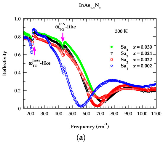
Figure 1.
(a) Experimental room-temperature (300 K) high-resolution infrared reflectance spectra of four gas-source MBE-grown zb InAs1−xNx/InP (001) samples (#Sa1, Sa2, Sa3 and Sa4) with different N composition x, revealing -like and -like modes shown by vertical magenta color arrows (see text). (b) Experimental room-temperature high-resolution infrared reflectance spectra of InP substrate (see text). (c) Experimental Raman scattering spectra of InP substrate (see text).
4.1. Reflectivity Spectra
The experimental results of IRR measurements at RT (see Figure 1a) on the GS-MBE-grown zb InAs1−xNx epifilms and InP substrate (Figure 1b) were obtained by using a high-resolution Brüker IFS 120 v/S FTIR spectrometer in the frequency range of ~150 cm−1 to 1100 cm−1. All the experimental measurements were performed with a 2 cm−1 resolution and the use of 100 coadditions. The Raman scattering study of the InP substrate at RT was also accomplished (see Figure 1c) in the double subtractive configuration by using a Jobin-Yvon T64000 spectrometer equipped with a liquid N2-cooled CCD.
The simulated results of IR reflectivity spectra of binary materials are displayed in Figure 2a using different color lines: black for InAs, red for InP, blue for InN and green for InAs0.97N0.03. We drew sky-blue color vertical arrows for binary (InAs, InP, InN) materials and grey color arrows for the InAs0.97N0.03 alloy to signify their respective Reststrahlen band regions. The perusal of Figure 2a clearly reveals that the spectrum of each binary material drops to a minimum value at the plasma edge and exhibits a peak near the phonon frequency. As expected, the calculated spectra of the ternary InAs0.97N0.03 alloy demonstrate two Reststrahlen peaks, one related to the InAs-like phonon region and the other related to the InN-like phonon region. However, the frequencies of - and -like modes overlap each other due to the small N composition x and are difficult to distinguish. This has also been confirmed by the simulated results of , and n, k (cf. Figure 2b,c). The calculations of , and n, k displayed in Figure 2b,c for InAs0.97N0.03 have revealed - and -like phonon energies at the peaks of , while the -like phonon mode has appeared near n = k, = 0.
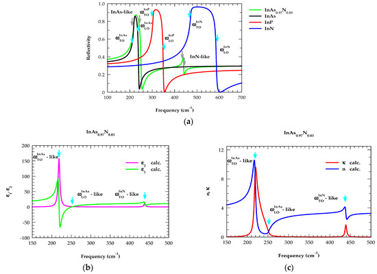
Figure 2.
(a) The simulated results of reflectivity spectra for InAs (black), InP (red), InN (blue) and InAs0.97N0.03 (green). Vertical arrows of different colors are drawn to signify their respective Reststrahlen band regions (e.g., sky blue for binary and grey for ternary InAs0.97N0.03 alloy). (b) The calculations of , and (c) n, κ for InAs0.97N0.03 revealed - and -like phonon energies at the peaks of while -like phonon modes appeared near n = k, = 0.
4.2. Reflectivity Spectra of InAs1−xNx Epifilms
In the framework of a standard methodology of multilayer optics and adopting a three-phase (ambient/film/substrate) model, we have studied the reflectivity spectra of four different GS-MBE-grown InAs1−xNx/inP (001) samples [40,41,42,43] having different thicknesses d and compositions (0.002 ≤ x ≤ 0.03). For each sample, the amplitude of the reflection coefficient or reflectivity R(ω) = ||2 is calculated at near-normal incidence (θi = 0) following the methodology reported in Section 3.2 [69]. The theoretical results displayed in Figure 3a–d are compared with the experimental data.
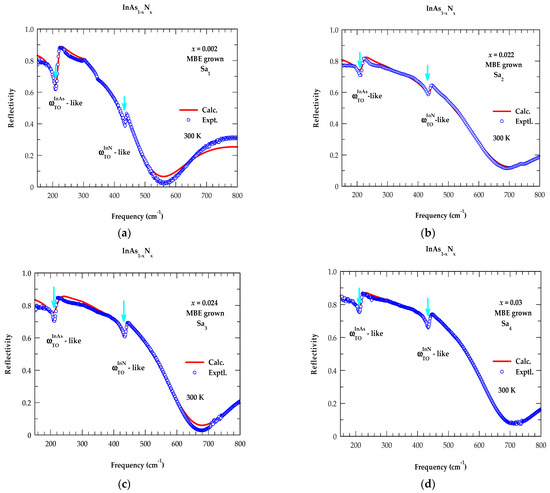
Figure 3.
(a) Comparison of the experimental (open circles) room-temperature infrared reflectance spectra of gas-source MBE-grown zb InAs1−xNx/InP (001) samples with the theoretical results (full lines) using the parameter values from Table 2, for (0.002); (b) same as (a) but for (0.022); (c) same as (a) but for (0.024); (d) same as (a) but for (0.03) (see text).
In the absence of accurate results of ε∞ and d for InAs1−xNx alloys, we have extracted these parameters by calculating/comparing the experimental reflectivity results using least-square fitting procedures, especially in the high-frequency region (1100 cm−1 ≥ ω > 500 cm−1). In Figure 4a,b, the simulated results of composition-dependent ε∞ and thickness d-dependent IRR spectra of InAs1−xNx/InP (for x = 0.002) are displayed, respectively. Similar calculations have also been performed for the other samples (not shown here), and the best-fit results of ε∞ and d are reported in Table 3. The estimated values of high-frequency dielectric constants ε∞ and epifilm thickness d for the InAs1−xNx alloys fall in the ranges of 11.32–12.76 and 2.460–2.670 μm, respectively. To fit the reflectivity spectra of the semi-insulating InP substrate ( = 0), we have used the value of ε∞ (≡9.61). The key parameters derived for the ternary alloy InAs1−xNx/InP (001) samples by fitting the RT reflectivity spectra are reported in Table 2 and Table 3. The elements included in the IRR simulations are the film thickness d; mobility μ; carrier concentration η; transverse-optical phonon frequencies , ; optical strengths ; damping constants , ; and effective mass .
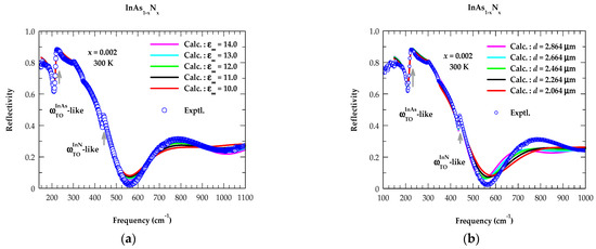
Figure 4.
Comparison of the experimental (open circles) room-temperature infrared reflectance spectra of GS-MBE-grown zb InAs1−xNx/InP (001) sample x = 0.002 (as an example) with the simulated (colored lines) spectra by varying (a) ε∞ and (b) d. The best-fit values are reported in Table 3.
From Table 2, one may note that all the intentionally undoped GS-MBE-grown zb InAs1−xNx samples exhibit n-type conduction. In Figure 5a,b, we display the impact of increasing N content x on the electron charge carrier concentration η, mobility μ and the effective electron mass (). In samples with the largest value of x = 0.03, it is quite surprising to notice that the effective mass estimated from the IRR fitting revealed a significantly large value of = 0.32.
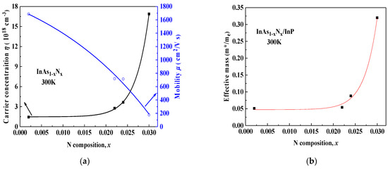
Figure 5.
(a) Simulated results of the N composition-dependent carrier concentration η, mobility μ and (b) effective mass ( estimated by fitting reflectivity spectra (Table 3) for InAs1−xNx/InP samples.
Although the maximum N content x, in InAs1−xNx is nearly 3%, we have noticed the effective electron mass increasing almost fourteen times from the nitrogen-free case of InAs ( = 0.023). The effective mass enhancement can be attributed to the size quantization, band nonparabolicity and the nitrogen-induced band structure modification. The origin of higher background n-type behavior in the intrinsic GS-MBE-grown zb InAs1−xNx samples is still under investigation. However, we speculate that (a) in InAs, the smaller-size N atoms (with larger host lattice constants) are possibly occupying the interstitial sites, and (b) in the narrower-bandgap InAs1−xNx, the defect levels are ionized. which might have resulted in the higher residual carrier density, η.
Again, from Table 3, it is obvious that the increase in x caused higher InAs-like TO1 phonon frequencies and damping constants Г1 and lower oscillator strengths S1. The increase in x also resulted in higher values of InN-like TO2 phonon frequencies, oscillator strengths S2 and damping constants Г2.
4.3. Berreman Effect
The articulation of simulating the IR reflectivity R(ω) = ||2 (transmission T(ω) = ||2) spectra at oblique incidence θi (≠0) is, however, a little more involved [82]. If an EM wave is incident on a film with an electric field polarized perpendicular to the plane of incidence (i.e., the s-wave), it interacts only with modes regardless of the angle of incidence θi. In contrast, both the and modes are excited by radiation that impinges on a film at an angle θi with an electric field polarized parallel to the plane of incidence (i.e., the p-wave) [83,84,85,86,87,88]. In such a situation, the electric field has a component in the direction of atomic motions for both the and phonons. In Figure 6a–c, we report our simulated results of IR reflectivity and transmission spectra in both the s- and p-polarization for InAs/InP (001), InN/InP (001) and InAs0.97N0.03/InP (001) epilayers of thickness d (≡0.2 μm) at an oblique incidence θi (≡45°), respectively.
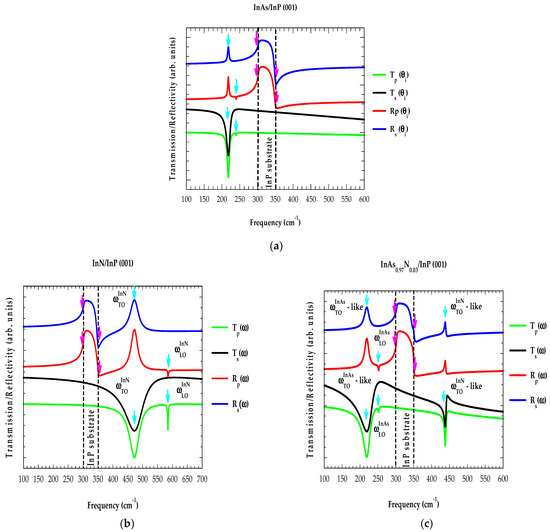
Figure 6.
(a) Simulated polarization-dependent transmission (lower panel) and reflectivity (upper panel) spectra of 0.2 μm thick InAs/InP epifilm, where the sky-blue color vertical arrows represent the and phonons while the magenta color vertical arrows signify the Reststrahlen region of InP (substrate); (b) same as (a) but for InN/InP epifilm; (c) same as (a) but for InAs0.97N0.03/InP epifilm (see text).
4.3.1. InAs/InP (001)
In Figure 6a, the results of IR reflectivity (red and blue color lines: upper panel) and transmission spectra (green and black color lines: lower panel) are reported in the s- and p-polarization for the InAs/InP (001) epifilm of thickness d (≡0.2 μm) at the incidence angle θi (≡45°). Clearly, the outcomes of the simulated spectra can be divided into two zones: (a) the InAs-like phonon region which falls between the mode frequencies of 219 and 243 cm−1 and (b) a broad InP-like Reststrahlen band region (see Figure 6a) of the substrate occurring in the range of ~305 to ~350 cm−1. While the reflectivity spectra of InP shown by magenta color vertical arrows remained nearly unaffected, the transmission and reflectivity spectra of InAs indicated by sky-blue color vertical arrows changed significantly in the s- and p-polarizations. Obviously, the simulations of ) spectra in p-polarization of the InAs/InP (001) epilayer (see Figure 6a) have confirmed the ωTO mode appearing at ~219 cm−1 as a distinct maximum (minimum). In addition, a sharp minimum is noticed emerging at a higher frequency indicating the ωLO mode at ~243 cm−1. In s-polarization, however, the simulated ) spectra revealed only the mode as a maximum (minimum), in excellent agreement with the XRTD [78] and RSS [83,84,85,86,87,88] results.
4.3.2. InN/InP (001)
In Figure 6b, we report the calculated results of reflectivity (red and blue color lines: lower panel) and transmission spectra (green and black color: upper panel) in the s- and p-polarization for the InN/InP (001) epifilm of thickness d (≡0.2 μm) at the incidence angle θi (≡45°). Like what was observed for InAs/InP (001), the reflectivity spectra in s- and p-polarization of InN/InP (001) also exhibited two separate phonon zones: (a) a broad InP-like Reststrahlen band region of the substrate indicated by sky-blue color vertical arrows occurring in the frequency range of ~305 cm−1 to ~350 cm−1 and (b) the InN-like phonon band region which falls within the mode frequencies of ~476 cm−1 to ~595 cm−1. While the reflectivity spectra of InP shown by magenta color vertical arrows remained nearly unaffected, the transmission and reflectivity spectra of the InN bands indicated by sky-blue color arrows are, however, perceived to significantly change in the s- and p-polarizations. Obviously, the simulations of ) spectra in the p-polarization of the InN/InP (001) epilayer (see Figure 6b) have confirmed the mode appearing at ~476 cm−1 as a distinct maximum (minimum). In addition, a sharp minimum is also seen emerging at a higher frequency indicating the mode of ~595 cm−1. In s-polarization, the simulated ) spectra, however, revealed only the mode as a maximum (minimum), in excellent agreement with the results of first-principles calculations [79] and Raman scattering spectroscopy measurements [83,84,85,86,87,88].
4.3.3. InAs0.97N0.03/InP (001)
Like the results presented for the InAs/InP (001) and InN/InP (001) epifilms (cf. Section 4.3.1 and Section 4.3.2), our simulated results of reflectivity and transmission spectra in the s- and p-polarization for an InAs0.97N0.03/InP (001) epilayer of thickness d (≡0.2 μm) at an oblique incidence θi (≡45°) are also reported in Figure 6c. Unlike binary materials (see Figure 6a,b), the calculated results of IR reflectivity (red and blue color lines: upper panel) and transmission spectra (green and black color lines: lower panel) of the InAs0.97N0.03 alloy epifilm exhibit three zones: (a) a broad InP-like Reststrahlen band region indicated by magenta color vertical arrows occurs in the frequency range of ~305 cm−1 to ~350 cm−1, (b) the InAs-like phonon band shown by sky-blue color vertical arrows falls between the mode frequencies of ~220 cm−1 and ~243 cm−1, and (c) the InN-like phonon mode region indicated by sky-blue color vertical arrows appears in the frequency range of ~441 cm−1 to ~443 cm−1. While the reflectivity spectra of InP shown by magenta color vertical arrows remained nearly unaffected, the transmission and reflectivity of InAs and InN bands shown by sky-blue color arrows are, however, perceived to change significantly in the s- and p-polarizations. Once again, our results of p-polarized ) spectra for the InAs0.97N0.03 /InP (001) epilayer (see: Figure 6c) have confirmed ωTO modes emerging as a distinct maximum (minimum) at ~220 cm−1 and ~441.0 cm−1, respectively. In addition, sharp minima appear at higher frequencies, indicating the mode of ~243 cm−1, while the InN-like mode, due to low x, was not fully resolved ( ~442 cm−1). In the s-polarization, however, the calculated ) spectra have revealed only the and modes as a maximum (minimum), in excellent agreement with the results from XRTD, [78] Raman scattering spectroscopy [83,84,85,86,87,88] and first-principles [79] calculations.
4.4. Lattice Dynamics of InAs and InN
By exploiting a realistic RIM [77] and using the optimized set of force constants (Table 4), we have calculated the phonon dispersions (see Figure 7a,b) and one-phonon density of states (DOS) (Figure 7c) for the bulk InAs and InN materials, respectively. The results reported in Figure 7a,b along the high-symmetry directions (Г → X → K → Г → L → X → W → L) are compared/contrasted reasonably well with the existing XRTD [78] and first-principles [79] calculations. The perusal of Figure 7a,b clearly reveals the correct separation between the acoustic and optical phonon branches where the lighter As and N atoms provided major contributions to the optical phonons while the heavier In atoms contributed effectively to the acoustic modes.
Table 4.
Optimized set of rigid-ion model parameters (105 dyn/cm) [77] for calculating the lattice dynamics of the zinc-blende InAs and InN materials.
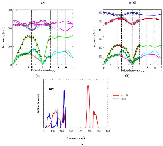
Figure 7.
Comparison (Table 4) of the rigid-ion model (RIM) calculation (full lines) of phonon dispersions for (a) InAs with the XRTD scattering data (shown by symbols), for (b) InN with first-principles calculation (shown by symbols). (c) Calculated one-phonon density of states for InAs and InN.
One may also note that going from As to N (i.e., from higher to lower atomic number), the optical phonon frequencies of InN increased with respect to the InAs material. This fact is also reflected in our simulations of the one-phonon DOS (Figure 7c) where a larger phonon gap is evidenced between the acoustic and optical branches of InN (~236–458 cm−1) as compared to the InAs (160–185 cm−1). Our results of and DOS for InN are in very good agreement with the first principles calculations [79] performed within the DFT formalism using local-density approximation.
4.4.1. ATM-GF Study of Impurity Modes of Donors/Acceptors in InAs and InN
The calculated phonons (eigenvalues and eigenfunctions) of the perfect InAs and InN are meticulously incorporated for simulating the Green’s functions of the host materials. Appropriate perturbation matrices are considered in the ATM-GF theory [73,74,75,76] for comprehending the impurity vibrational modes [53,54,55,56,57] of different isoelectronic donors and acceptors in InAs and InN. In the nearest-neighbor (NN) configuration (Td-symmetry), it is possible to obtain the LVM frequencies of isolated light defects occupying either the cation or anion sites in various irreducible representations (μΓ: A1, E, F2) by solving the following equation [73]:
The results of ATM-GF calculations will help us identify the observed LVMs of donors and and acceptors in InAs [53,54,55,56,57] and provide clarification to the ambiguous picture of impurity modes for and acceptors and donors in InN [58,59,60,61,62,63,64,65,66,67,68]. Here, we discuss the following cases.
4.5. LVMs of Isolated Defects in InAs and zb InN
In InAs, the light Si impurities are amphoteric, i.e., they act as donors when occupying the In sites and acceptors if substituted on the As sites. By using Raman scattering spectroscopy, Uematsu [54] has confirmed the observation of the LVMs of isolated 28 donors and 28 acceptors with Td-symmetry as well as a donor–acceptor pair 28- 28 mode of C3v-symmetry. In InN, one also expects 28 to act as a donor and 26 and 12 as acceptors. Except for 12 in InAs [53,54,55,56,57], conflicting reports of impurity modes are known for the 26 acceptors in InN, while no LVM results are available for isolated 28 donors and 12 acceptors [58,59,60,61,62,63,64,65,66,67,68].
Calculations of impurity modes using ATM-GF theory require accurate perturbation matrices with mass ε1 (ε2) and force-constant change t (u) parameters [73] for the defects occupying In (As or N) sites in InAs and InN. If we assume that only the NN lattice sites are perturbed by the presence of isolated substitutional defects, then the decomposition of a 15 × 15 total representation of Equation (4) in a given irreducible representation (A1, E, F1 and F2) can be expressed as follows [73]:
Г(Td) = A1 + E + F1 + 3F2.
One must note that an irreducible representation that transforms like a polar vector is infrared-active. In this situation, the triply degenerate F2 mode is IR-active while the A1, E and F2 modes are Raman-active. To simulate the LVMs of light impurities in semiconductors, we have first estimated the lattice relaxations around each defect by using a first-principles bond-orbital model (BOM) [89]. The second derivatives of bond energies enabled us to assess the force-constant variations t (u) for 28 donor and (28, 2612, 12) acceptor defects in InAs and InN matrices. Appropriate force-constant and mass change parameters of isolated impurities are used to establish the perturbation matrices while the necessary GFs () of the host lattices are obtained by integrating the RIM [77] phonons fitted to the XRTD data of InAs [78] and the first-principles data of InN [79]. The LVM frequencies of several isolated impurities in III-V compounds are obtained in Raman- and IR-active F2 irreducible representation using Equation (4) from the zeroes of the real part of the determinant.
After meticulously analyzing [76] the Raman scattering and infrared spectroscopy data [53,54,55,56,57] of many isolated defects in semiconductors, we noticed large variations in the impurity–host interaction parameters ∆t and (∆u) between the closest mass isoelectronic i and donor d+ (i and acceptor a−) occupying the III and (V) sites in III-V compounds, i.e., strong stiffening with ∆t < 0 and (∆u (). However, for the closest mass isoelectronic i and acceptor a− (i and donor d+) occupying the III and (V) sites in III-V compounds, the study has provided strong softening (i.e., ∆t ( > 0 and (∆u ()). These observations have convincingly suggested that the charged impurities in semiconductors can only affect the short-range forces via the redistribution of electron charge density [76].
With the choice of appropriate values of both the mass change ε1 (ε2) and force-constant change t (u) parameters, the LVMs of light impurities occupying either In or (As, N) sites are calculated from the crossing of zeroes (Equation (4)) above the maximum phonon frequencies of InAs (InN) ~243 cm−1 (~595 cm−1). For InAs, our results have provided the LVMs of the 28 donors (28) near ~359 cm−1 (~328 cm−1) and the 12 acceptors at ~530 cm−1, offering strong corroborations of the existing experimental [53,54,55,56,57] data. Recent RSS and FTIR [54] measurements of the isotopic shifts by ~19 cm−1 for 12 (13) modes also supported our predictions that the LVM near ~530 cm−1 is related to the isolated 12-acceptor in InAs. Due to the weak 26-N bonding as compared to the strong 28-N bonding, our ATM-GF theory has predicted the vibrational mode of 26 (acceptor) to fall in the band mode region (~569 cm−1) and 28 (donor) to appear just above the . While the impurity vibrational mode for the 26 in InN agrees very well with the existing RSS data [49], we, however, assigned this as an impurity-activated phonon mode, and certainly, it is not the LVM. There also exist many other studies conducted to comprehend the role of Mg dopants η (1 × 10¹⁶ to 4 × 1021 cm−3) in InN [58,59,60,61,62,63,64,65,66,67,68]. Besides the strain-induced modes, the observation of high-frequency LVMs involving Mg-H complexes confirmed the evidence of p-type conduction in InN. The possible occupation of Mg impurities and their site selectivity were also investigated by Chen et al. [58] using a diffusion–collision model of LVMs. For the Mg concentration η < 1.8 × 1020 cm−3, the authors [58] argued that the dominant defects are either Mgi interstitials and/or MgIn-N-Ini complexes. By increasing the Mg concentration to η > 2 × 1020 cm−3, the authors suggested the formation of MgIn-N-Mgi centers which can cause high-frequency impurity vibrational modes [58].
Again, C impurities are often present in the growth process of III-nitrides. Unlike III-V materials, the role of C in AlN, GaN and InN is not fully understood [58,59,60,61,62,63,64,65,66,67,68]. Many electronic and phonon energy calculations of C defects using first-principles density functional methods are known in the literature [58,59,60,61,62,63,64,65,66,67,68]. These calculations indicated that carbon in the interstitial Ci site in InN is stable and contributes to n-type conduction [65,68]. Due to a short bond length between C-N split interstitials, the predicted stretching C-N mode near ~2270 cm−1 [68] should be observed by FTIR and/or RSS spectroscopy.
4.6. Longitudinal Optical–Plasmon Coupling Modes in n-Doped InN
One must note that both Raman scattering and infrared spectroscopies [53,54,55,56,57,58,59,60,61,62,63,64,65,66,67,68] are considered the most powerful and complementary tools for investigating the lattice dynamical properties of semiconductor materials, including (a) the estimation of doping concentration, (b) the identification of the site selectivity of defects, (c) the study of crystal orientation, and (d) comprehending the phonon dynamics. Being a nondestructive and contactless method, RSS is especially valuable for probing the free charge carrier concentration in nanostructured Si-doped InN nanowires [58,59,60,61,62,63,64,65,66,67,68]. In the framework of “Drude–Lorentz” model (Section 3.4), the calculated results of the modes in n-InN are displayed in Figure 8 as a function of the charge carrier concentration η (1 × 10¹⁷–2 × 1021 cm−3).
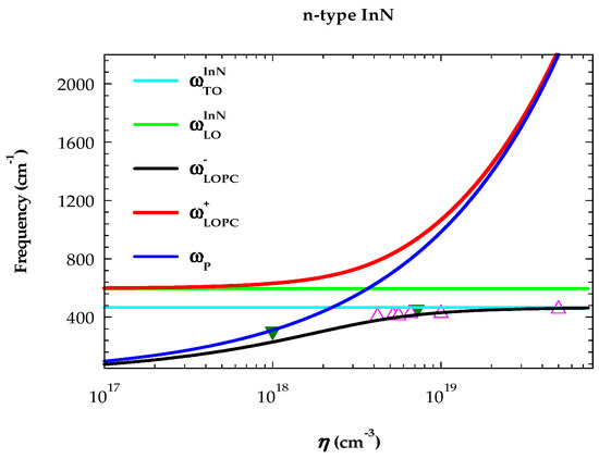
Figure 8.
Calculated results of LO-phonon plasmon coupled () modes in heavily Si-doped InN (see text) as a function of charge carrier concentration η (cm−3). Symbols represent the Raman scattering experimental data of .
Using the visible 514.5 nm and UV 325 nm energy excitations, Raman scattering spectroscopy measurements have detected a weak vibrational mode in Si-doped InN between ~375 and 450 cm−1 [58,59,60,61,62,63,64,65,66,67,68]. As η is increased, the Si-related mode shifts upwards and its line shape is sharpened, attaining a phonon-like character (), confirming our calculations (see Figure 8)). While no mode has been detected, a weak and broad band near ~600 cm−1 is linked, however, to the disorder-activated longitudinal optical mode (DALO) [58,59,60,61,62,63,64,65,66,67,68]. These experimental observations have completely supported our ATM-GF calculations for the impurity mode characteristics of 28 donors in InN.
5. Concluding Remarks
We have successfully grown zb InAs1−xNx/InP (001) epilayers of different N composition x by using the GS-MBE technique. High-resolution IR reflectivity measurements have revealed a -like phonon line near ~219 cm−1 and an LVM mode at ~439 cm−1 linked to an isoelectronic 14. Based on our comprehensive ATM-GF theory (Section 4.4.1), (a) nearly ~30% force-constant stiffening (∆u () is noticed between the closest mass C-acceptor “13” and N-isoelectronic “14” bonds. In InAs, this force variation provided an accurate shift in 12LVM frequency from ~530 cm−1 to a lower value, ~511 cm−1, for the 13isotopic defect. Compared to the local mode of 14isoelectronic mass, our ATM-GF result for 13 acceptor agreed very well with the FTIR [53] results. On the contrary, our study of 26 and 28 in InN has revealed weaker “26-N” and stronger “28-N” bonding compared to the closest mass isoelectronic 27 defect. Accordingly, the simulation of impurity vibrations for 26 and 28 has predicted lower and higher values at ~569 cm−1 and ~600 cm−1, respectively. While the vibrational frequency of 26 in InN agrees very well with the Raman scattering result [49], we feel that this mode needs to be re-assigned as an impurity-activated phonon and certainly not as an LVM. Besides the ATM-GF calculations of impurity modes, the reflectivity/transmission studies at oblique incidence in InAs1−xNx/InP (001) epilayers have confirmed the perception of ωTO phonons in s-polarization and ωTO and ωLO modes in p-polarization. Consistent with infrared and Raman scattering measurements [53,54,55,56,57], our results have established the impurity identification and characterization of 14 (isoelectronic) 13, 28 and 28 in InAs [53,54,55,56,57]. The predicted impurity vibrational modes for 28 (donor) and 26 (acceptor) in InN also agreed reasonably well with the existing spectroscopic data. We strongly feel that our systematic theoretical approach can be equally valuable for studying the lattice dynamics of other technologically important perfect and imperfect semiconductors.
Author Contributions
D.N.T., conceptualization, methodology, investigation, computational analysis, writing original draft. T.-R.Y., infrared measurements on GS-MBE samples. H.-H.L., supervision, GS-MBE growth, characterization, editing. All authors have read and agreed to the published version of the manuscript.
Funding
This research has received no external funding.
Institutional Review Board Statement
Not applicable.
Informed Consent Statement
Not applicable.
Data Availability Statement
The data that support the findings of this study are available from the corresponding author upon reasonable request.
Acknowledgments
The author (DNT) wishes to thank Deanne Snavely, Dean College of Natural Science and Mathematics at Indiana University of Pennsylvania (IUP), for the travel support and the Innovation Grant that he received from the School of Graduate Studies making this research possible. The author HHL would like to acknowledge the financial support from the National Science and Technology Council, R.O.C, under Contract No. NSC 89-2215-E-002-034 and NSTC 112-2221-E-002-250. HHL also wishes to thank D. K. Shih for the GSMBE growth.
Conflicts of Interest
The authors declare that they have no financial interests/personal relationships that may be considered as potential competing interests.
References
- Mawst, L.J.; Kim, H.; Smith, G.; Sun, W.; Transu, N. Strained-layer quantum well materials grown by MOVCD for diode laser applications. Prog. Quantum Electron. 2021, 75, 100303. [Google Scholar] [CrossRef]
- Grillot, F.; Duan, J.; Dong, B.; Huang, H. Un covering recent progress in nanostructured light-emitters for information and communication technologies. Light Sci. Appl. 2021, 10, 156. [Google Scholar] [CrossRef]
- Chaves, A.; Azadani, J.G.; Alsalman, H.; da Costa, D.R.; Frisenda, R.; Chaves, A.J.; Song, S.H.; Kim, Y.D.; He, D.; Zhou, J.; et al. Bandgap engineering of two-dimensional semiconductor materials. NPJ 2D Mater. Appl. 2020, 4, 29. [Google Scholar] [CrossRef]
- Peacock, A.C.; Sparks, J.R.; Healy, N. Semiconductor optical fibres: Progress and opportunities. Laser Photonics Rev. 2014, 8, 53–72. [Google Scholar] [CrossRef]
- Patanè, A.; Balkan, N. (Eds.) Semiconductor Research, Experimental Techniques; Springer Series in Materials Science; Springer: Berlin/Heidelberg, Germany, 2012; p. 150. [Google Scholar]
- Laidig, W.D.; Caldwell, P.J.; Lin, Y.F.; Peng, C.K. Strained-layer quantum-well injection laser. Appl. Phys. Lett. 1984, 44, 653–655. [Google Scholar] [CrossRef]
- Laidig, W.D.; Lin, Y.F.; Caldwell, P.J. Properties of InxGa1−xAs-GaAs strained-layer quantum-well-heterostructure injection lasers. J. Appl. Phys. 1985, 57, 33–38. [Google Scholar] [CrossRef]
- Moser, A.; Oosenbrug, A.; Latta, E.E.; Forster, T.; Gasser, M. High-power operation of strained InGaAs/AlGaAs single quantum well lasers. Appl. Phys. Lett. 1991, 59, 2642–2644. [Google Scholar] [CrossRef]
- York, P.K.; Beernink, K.J.; Fernandez, G.E.; Coleman, J.J. InGaAs-GaAs-AlGaAs strained-layer quantum well lasers by metal-organic chemical vapour deposition. Semicond. Sci. Technol. 1990, 5, 508–511. [Google Scholar] [CrossRef]
- Houle, F.A.; Neiman, D.L.; Tang, W.C.; Rosen, H.J. Chemical changes accompanying facet degradation of AlGaAs quantum well lasers. J. Appl. Phys. 1992, 72, 3884–3896. [Google Scholar] [CrossRef]
- de la Mare, M.; Zhuang, Q.; Patane, A.; Krier, A. Effects of substrate and N content on the growth of the mid-infrared dilute nitride InAsN alloy. J. Phys. D Appl. Phys. 2012, 45, 395103. [Google Scholar] [CrossRef]
- Wang, D.; Svensson, S.P.; Shterengas, L.; Belenky, G. Near band edge optical absorption and photoluminescence dynamics in bulk InAsN dilute-nitride materials. J. Cryst. Growth 2010, 312, 270–275. [Google Scholar] [CrossRef]
- Debbichi, M.; Fredj, A.B.; Cuminal, Y.; Lazzari, J.-L.; Ridene, S.; Bouchriha, H.; Saïd, M.; Christol, P. InAsN/GaSb/InAsN ‘W’ quantum well laser for mid-infrared emission: From electronic structure to threshold current density calculations. J. Phys. D Appl. Phys. 2008, 41, 215106. [Google Scholar] [CrossRef]
- Chalker, P.R.; Bullough, T.J.; Gass, M.; Thomas, S.; Joyce, T.B. The microstructural influence of nitrogen incorporation in dilute nitride semiconductors. J. Phys. Condens. Matter 2004, 16, S3161–S3170. [Google Scholar] [CrossRef]
- Pettinari, G.; Felici, M.; Biccari, F.; Capizzi, M.; Polimeni, A. Site-Controlled Quantum Emitters in Dilute Nitrides and their Integration in Photonic Crystal Cavities. Photonics 2018, 5, 10. [Google Scholar] [CrossRef]
- Welser, R.E.; Setzko, R.S.; Stevens, K.S.; Rehder, E.M.; Lutz, C.R.; Hill, D.S.; Zampardi, P.J. Minority carrier properties of carbon doped GaInAsN bipolar transistors. J. Phys. Condens. Matter 2004, 16, S3373–S3385. [Google Scholar] [CrossRef]
- Potter, R.J.; Balkan, N. Optical properties of GaNAs and GaInAsN quantum wells. J. Phys. Condens. Matter 2004, 16, S3387–S3412. [Google Scholar] [CrossRef]
- Taliercio, T.; Valvin, P.; Intartaglia, R.; Sallet, V.; Harmand, J.C.; Guillet, T.; Lefebvre, P.; Bretagnon, T.; Gil, B. Continuous wave and time resolved spectroscopy of InAsN/GaAsN based quantum dots. Phys. Stat. Sol. A 2005, 202, 2598–2603. [Google Scholar] [CrossRef]
- Filippone, F.; Mattioli, G.; Polimeni, A.; Felici, M.; Bonapasta, A. Opposite Hydrogen Behaviors in GaAsN and InAsN Alloys: Band Gap Opening versus Donor Doping. J. Phys. Chem. C 2020, 124, 19240–19251. [Google Scholar] [CrossRef]
- Oriaku, C.I.; Spencer, T.J.; Yang, X.; Zubelli, J.P.; Pereira, M.F. Analytical Expressions for the Luminescence of Dilute Quaternary InAs(N, Sb) Semiconductors. J. Nano Photonics 2017, 11, 026005. [Google Scholar] [CrossRef]
- Xie, Z.; Sui, Y.; Buckeridge, J.; Catlow, C.R.A.; Keal, T.W.; Sherwood, P.; Walsh, A.; Farrow, M.R.; Scanlon, D.O.; Woodley, S.M.; et al. Donor and acceptor characteristics of native point defects in GaN. J. Phys. D Appl. Phys. 2019, 52, 335104. [Google Scholar] [CrossRef]
- Bhusal, L.; Freundlich, A. GaAsN/InAsN superlattice based multijunction thermophotovoltaic devices. J. Appl. Phys. 2007, 102, 074907. [Google Scholar] [CrossRef]
- Gründl, T.; Böhm, G.; Meyer, R.; Amann, M.-C. GaInAsN growth studies for InP-based long-wavelength laser applications (TUA3-3). J. Cryst. Growth 2009, 311, 1719–1722. [Google Scholar] [CrossRef]
- Seravalli, L.; Sacconi, F. Reviewing quantum dots for single-photon emission at 1.55 µm: A quantitative comparison of materials. J. Phys. Mater. 2020, 3, 042005. [Google Scholar]
- Ougazzaden, A.; Bellego, Y.L.; Rao, E.V.K.; Juhel, M.; Leprince, L.; Patriarche, G. Metal organic vapor phase epitaxy growth of GaAsN on GaAs using dimethyl hydrazine and tertiary butyl arsine. Appl. Phys. Lett. 1997, 70, 2861. [Google Scholar] [CrossRef]
- Gilet, P.; Paule, A.C.; Duvaut, P.; Grenouillet, L.; Holliger, P.; Million, A.; Rolland, G.; Vannuffel, C. Growth and Characterization of Thick GaAsN Epilayers and GaInNAs/GaAs Multi-quantum Wells. Phys. Stat. Sol. A 1999, 176, 279. [Google Scholar] [CrossRef]
- Ikeda, K.; Xiuxun, H.; Boussairi, B.; Ohshita, Y. GaAsN Grown by Chemical Beam Epitaxy for Solar Cell Application; Intech: London, UK, 2013; Volume 282. [Google Scholar] [CrossRef]
- Ściana, B.; Pucicki, D.; Radziewicz, D.; Serafińczuk, J.; Kozłowski, J.; Paszkiewicz, B.; Tłaczała, M.; Poloczek, P.; Sęk, G.; Misiewicz, J. APMOVPE growth and haracterization of undoped GaAsN/GaAs heterostructures. Vacuum 2008, 82, 377–382. [Google Scholar] [CrossRef]
- Ściana, B.; Zborowska-Lindert, I.; Pucicki, D.; Boratyński, B.; Radziewicz, D.; Tłaczała, M.; Serafińczuk, J.; Poloczek, P.; Sęk, G. Technology and characterization of GaAsN/GaAs heterostructures for photodetector applications. Opto Electron. Rev. 2008, 16, 1–7. [Google Scholar] [CrossRef]
- Ściana, B.; Dawidowski, W.; Radziewicz, D.; Jadczak, J.; López-Escalante, M.C.; González de la Cruz, V.; Gabás, M. Influence of As-N Interstitial Complexes on Strain Generated in GaAsN Epilayers Grown by AP-MOVPE. Energies 2022, 15, 3036. [Google Scholar] [CrossRef]
- Gao, Q.; Tan, H.H.; Jagadish, C.; Sun, B.Q.; Gal, M.; Ouyang, L.; Zou, J. Enhanced optical properties of the GaAsN/GaAs quantum-well structure by the insertion of InAs monolayers. Appl. Phys. Lett. 2004, 84, 2536. [Google Scholar] [CrossRef]
- Reentila, O.; Lankinen, A.; Mattila, M.; Saynatjoki, A.; Tuomi, T.O.; Lipsanen, H.; O’Reilly, L.; McNally, P.J. In-situ optical reflectance and synchrotron X-ray topography study of defects in epitaxial dilute GaAsN on GaAs. J. Mater. Sci. Mater. Electron. 2008, 19, 137–142. [Google Scholar] [CrossRef]
- Pulzara-Mora, A.; Cruz-Hernández, E.; Rojas-Ramirez, J.; Contreras-Guerrero, R.; Meléndez-Lira, M.; Falcony-Guajardo, C.; López-López, M.; Aguilar-Frutis, M.A.; Vidal, M.A. Characterization of optical and structural properties of GaAsN layers grown by Molecular Beam Epitaxy. Superf. Vacío. 2005, 18, 27–32. [Google Scholar]
- de la Mare, M.; Zhuang, Q.; Krier, A.; Patanè, A.; Dhar, S. Growth and characterization of InAsN/GaAs dilute nitride semiconductor alloys for the midinfrared spectral range. Appl. Phys. Lett. 2009, 95, 031110. [Google Scholar] [CrossRef]
- Wheatley, R.; Kesaria, M.; Mawst, L.J.; Kirch, J.D.; Kuech, T.F.; Marshall, A.; Zhuang, Q.D.; Krier, A. Extended wavelength mid-infrared photoluminescence from type-I InAsN and InGaAsN dilute nitride quantum wells grown on InP. Appl. Phys. Lett. 2015, 106, 232105. [Google Scholar] [CrossRef]
- Shono, T.; Mizuta, S.; Kawamura, Y. Optical properties of InAsSbN single quantum wells grown on InP substrates for 2-mm-wavelength region. J. Cryst. Growth 2013, 378, 69. [Google Scholar] [CrossRef]
- Inoue, N.; Kawamura, Y. Infrared defect dynamics—Nitrogen-vacancy complexes in float zone grown silicon introduced by electron irradiation. J. Appl. Phys. 2018, 123, 185701. [Google Scholar] [CrossRef]
- Kawamura, Y. InP-based InGaAsSbN quantum well laser diodes in the 2-μm wavelength region. Electron. Commun. Jpn. 2011, 94, 33. [Google Scholar] [CrossRef]
- Kawamura, Y.; Inoue, N. Electroluminescence of In0.53Ga0.47As0.99N0.01/GaAs0.5Sb0.5 Type-II Quantum Well Light-Emitting Diodes Grown on InP Substrates by Molecular Beam Epitaxy. Jpn. J. Appl. Phys. 2007, 46, 3380–3381. [Google Scholar]
- Shih, D.-K.; Lin, H.-H.; Lin, Y.H. InAs0.97N0.03/InGaAs/InP multiple quantum-well lasers with emission wavelength λ = 2.38 µm. Electron. Lett. 2001, 37, 1342. [Google Scholar]
- Chen, G.R.; Lin, H.H.; Wang, J.S.; Shih, D.K. Optical properties of InAs1−xNx/In0.53Ga0.47 As single quantum wells grown by gas source molecular beam epitaxy. J. Electron. Mater. 2003, 32, 244. [Google Scholar] [CrossRef]
- Hang, D.R.; Shih, D.K.; Huang, C.F.; Hung, W.K.; Chang, Y.H.; Chen, Y.F.; Lin, H.H. Large effective mass enhancement of the InAs1−xNx alloys in the dilute limit probed by Shubnikov-de Haas oscillations. Physica E 2004, 22, 308–311. [Google Scholar] [CrossRef]
- Wang, J.S.; Lin, H.H. Growth and postgrowth rapid thermal annealing of InAsN/InGaAs single quantum well on InP grown by gas source molecular beam epitaxy. J. Vac. Sci. Technol. B 1999, 17, 1997. [Google Scholar] [CrossRef][Green Version]
- Wang, S.Z.; Yoon, S.F.; Fan, W.J.; Liu, C.Y.; Yuan, S. Thermal excitation effects of photoluminescence of annealed quantum-well laser structures grown by plasma-assisted molecular-beam epitaxy. J. Vac. Sci. Technol. B 2005, 23, 1434. [Google Scholar] [CrossRef]
- Kawamura, Y.; Sahashi, T. 2.86 µm room-temperature light emission of InGaAsN/GaAsSb type-II quantum well diodes grown on InP substrates. Jpn. J. Appl. Phys. Part 1 2014, 53, 028004. [Google Scholar] [CrossRef]
- Kawamata, S.; Hibino, A.; Tanaka, S.; Kawamura, Y. Effective mass of two-dimensional electrons in InGaAsN/GaAsSb type II quantum well by Shubnikov-de Haas oscillations. J. Appl. Phys. 2016, 120, 142109. [Google Scholar] [CrossRef]
- Cabrera-Montealvo, J.J.; Espinosa-Vega, L.I.; Hernàndez-Gaytan, L.M.; Mercado-Ornelas, C.A.; Perea-Parrales, F.E.; Belio-Manzano, A.; Yee-Rendon, C.M.; Rodríguez, A.G.; Mèndez-García, V.H.; Cortes-Mestizo, I.E. Strain and annealing temperature effects on the optical properties of GaNAs layers grown by molecular beam epitaxy. Thin Solid Film. 2022, 748, 139147. [Google Scholar] [CrossRef]
- Zhang, Y.; Fluegel, B.; Hanna, M.C.; Geisz, J.F.; Wang, L.-W.; Mascarenhas, A. Effects of heavy nitrogen doping in III–V semiconductors—How well does the conventional wisdom hold for the dilute nitrogen “III–V-N alloys”? Phys. Stat. Sol. B 2003, 240, 396–403. [Google Scholar] [CrossRef]
- Lee, H.S.; Ng, S.S.; Yam, F.K. Sol–gel spin coating growth of magnesium-doped indium nitride thin films. Vacuum 2018, 155, 16–22. [Google Scholar] [CrossRef]
- Inushima, T.; Higashiwaki, M.; Matsui, T. Optical properties of Si-doped InN grown on sapphire (0001). Phys. Rev. B 2003, 68, 235204. [Google Scholar] [CrossRef]
- Cuscó, R.; Domènech-Amador, N.; Artús, L.; Gotschke, T.; Jeganathan, K.; Stoica, T.; Calarco, R. Probing the electron density in undoped, Si-doped, and Mg-doped InN nanowires by means of Raman scattering. Appl. Phys. Lett. 2010, 97, 221906. [Google Scholar] [CrossRef]
- Wang, J.B.; Li, Z.F.; Chen, P.; Lu, W.; Yao, T. Raman study of gap mode and lattice disorder effect in InN films prepared by plasma-assisted molecular beam epitaxy. Acta Mater. 2007, 55, 183–187. [Google Scholar] [CrossRef]
- Najmi, S.; Chen, X.K.; Yang, A.; Steger, M.; Thewalt, M.L.W.; Watkins, S.P. Local vibrational mode study of carbon doped InAs. Phys. Rev. B 2006, 74, 113202. [Google Scholar] [CrossRef]
- Uematsu, M. Raman scattering of Si localized vibrational modes in InAs. J. Appl. Phys. 1991, 69, 1781. [Google Scholar] [CrossRef]
- Ibáñez, J.; Oliva, R.; De la Mare, M.; Schmidbauer, M.; Hernández, S.; Pellegrino, P.; Scurr, D.J.; Cuscó, R.; Artús, L.; Shafi, M.; et al. Structural and optical properties of dilute InAsN grown by molecular beam epitaxy. J. Appl. Phys. 2010, 108, 103504. [Google Scholar] [CrossRef]
- Newman, R.C. Local vibrational mode spectroscopy of defects in III/V compounds. In Semiconductors and Semimetals; Weber, E., Ed.; Academic Press: New York, NY, USA, 1993; Volume 38, pp. 117–181. [Google Scholar]
- Stavola, M. Vibrational Spectroscopy of Light Element Impurities in Semiconductors. In Semiconductors and Semimetals; Stavola, M., Ed.; Academic Press: New York, NY, USA, 1999; Volume 51, pp. 153–224. [Google Scholar]
- Chen, Z.; Sui, J.; Wang, X.; Kim, K.; Wang, D.; Wang, P.; Wang, T.; Rong, X.; Harima, H.; Yoshikawa, A.; et al. Transition of dominant lattice sites of Mg in InN: Mg revealed by Raman scattering. Superlattices Microstruct. 2018, 120, 533–539. [Google Scholar] [CrossRef]
- Davydov, V.Y.; Klochikhin, A.A.; Smirnov, M.B.; Smirnov, A.N.; Goncharuk, I.N.; Kurdyukov, D.A.; Lu, H.; Schaff, W.J.; Lee, H.M.; Lin, H.W.; et al. Experimental and theoretical studies of lattice dynamics of Mg-doped InN. Appl. Phys. Lett. 2007, 91, 111917. [Google Scholar] [CrossRef]
- Davydov, V.Y.; Klochikhin, A.A.; Smirnov, M.B.; Kitaev, Y.E.; Smirnov, A.N.; Lundina, E.Y.; Lu, H.; Schaff, W.J.; Lee, H.M.; Lin, H.W.; et al. SIMS and Raman studies of Mg-doped InN. Phys. Status Solidi C 2008, 5, 1648–1651. [Google Scholar] [CrossRef]
- Wang, X.Q.; Che, S.B.; Ishitani, Y.; Yoshikawa, A. Experimental determination of strain-free Raman frequencies and deformation potentials for the E2(high) and A1(LO) modes in hexagonal InN. Appl. Phys. Lett. 2006, 89, 171907. [Google Scholar] [CrossRef]
- Wright, A.F. Substitutional and interstitial carbon in wurtzite GaN. J. Appl. Phys. 2002, 92, 2575. [Google Scholar] [CrossRef]
- Ramos, L.E.; Furthmuller, J.; Leite, J.R.; Scolfaro, L.M.R.; Bechstedt, F. Carbon-based defects in GaN: Doping behavior. Phys. Status Solidi B 2002, 234, 864. [Google Scholar] [CrossRef]
- Eberlein, T.A.G.; Jones, R.; Oberg, S.; Briddon, P.R. Shallow acceptors in GaN. Appl. Phys. Lett. 2007, 91, 132105. [Google Scholar] [CrossRef]
- Duan, X.M.; Stampfl, C. Defect complexes and cluster doping of InN: First-principles investigations. Phys. Rev. B 2009, 79, 035207. [Google Scholar] [CrossRef]
- Bogusławski, P.; Bernholc, J. Doping properties of C, Si, and Ge impurities in GaN and AlN. Phys. Rev. B 1997, 56, 9496. [Google Scholar] [CrossRef]
- Fara, A.; Bernardini, F.; Fiorentini, V. Theoretical evidence for the semi-insulating character of AlN. J. Appl. Phys. 1999, 85, 2001. [Google Scholar] [CrossRef][Green Version]
- Lyons, J.L.; Janotti, A.; Van de Walle, C.G. Effects of carbon on the electrical and optical properties of InN, GaN, and AlN. Phys. Rev. B 2014, 89, 035204. [Google Scholar] [CrossRef]
- Talwar, D.N.; Yang, T.-R.; Feng, Z.C.; Becla, P. Infrared reflectance and transmission spectra in II-VI alloys and superlattices. Phys. Rev. B 2011, 84, 174203. [Google Scholar] [CrossRef]
- Maradudin, A.A.; Montroll, E.W.; Weiss, G.H.; Ipatova, I.P. Solid State Physics, 2nd ed.; Seitz, F., Turnbull, D., Ehrenreich, H., Eds.; Academic Press: New York, NY, USA, 1971. [Google Scholar]
- Elliott, R.J.; Krumhansl, J.A.; Leath, P.L. The theory and properties of randomly disordered crystals and related physical systems. Rev. Mod. Phys. 1974, 46, 465. [Google Scholar] [CrossRef]
- Kubo, R.J. Statistical-Mechanical Theory of Irreversible Processes. I. General Theory and Simple Applications to Magnetic and Conduction Problems. Phys. Soc. Jpn. 1957, 12, 570. [Google Scholar] [CrossRef]
- Talwar, D.N.; Feng, Z.C.; Lee, J.-F.; Becla, P. Structural and dynamical properties of Bridgman-grown CdSexTe1−x (0 < x ≤ 0.35) ternary alloys. Phys. Rev. B 2013, 87, 165208. [Google Scholar]
- Talwar, D.N.; Becla, P. Assessment of optical phonons in BeTe, BexZn1−xTe, p-BeTe epilayers, and BeTe/ZnTe/GaAs (001) superlattices. Appl. Phys. A 2022, 128, 702. [Google Scholar] [CrossRef]
- Talwar, D.N.; Becla, P. Interfacial strain-dependent localization of phonons in (CdS)m/(CdTe)n superlattices. Physica B 2023, 650, 414500. [Google Scholar] [CrossRef]
- Talwar, D.N. Dilute III-V Nitride Semiconductors and Material Systems: Physics and Technology; Erol, A., Ed.; Springer Series in Materials Science; Springer: Berlin/Heidelberg, Germany, 2008; Volume 105, Chapter 9; p. 222. [Google Scholar]
- Kunc, K. Dynamique de réseau de composés ANB8−N présentant la structure de la blende. Ann. Phys. 1973, 8, 319. [Google Scholar] [CrossRef]
- Orlova, N.S. Variation of phonon dispersion curves with temperature in indium arsenide measured by X-ray thermal diffuse scattering. Phys. Stat. Solidi B 1981, 103, 115–121. [Google Scholar] [CrossRef]
- Bechstedt, F.; Grossner, U.; Furthmuller, J. Dynamics and polarization of group-III nitride lattices: A first-principles study. Phys. Rev. B 2000, 62, 8003. [Google Scholar] [CrossRef]
- Plumelle, P.; Vandevyver, M. Lattice Dynamics of ZnTe and CdTe. Phys. Stat. Sol. 1976, 73, 271. [Google Scholar] [CrossRef]
- Matthews, J.W.; Blakeslee, A.E. Defects in epitaxial multilayers: I. Misfit dislocations. J. Cryst. Growth 1974, 27, 118. [Google Scholar] [CrossRef]
- Piro, O.E. Optical properties, reflectance, and transmittance of anisotropic absorbing crystal plates. Phys. Rev. B 1987, 36, 3427. [Google Scholar] [CrossRef] [PubMed]
- Berreman, D.W. Infrared absorption at longitudinal optic frequency in cubic crystal films. Phys. Rev. 1963, 130, 2193. [Google Scholar] [CrossRef]
- Sciacca, M.D.; Mayur, A.J.; Oh, E.; Ramdas, A.K.; Rodriguez, S.; Furdyna, J.K.; Melloch, M.R.; Beetz, C.P.; Yoo, W.S. Infrared observation of transverse and longitudinal polar optical modes of semiconductor films: Normal and oblique incidence. Phys. Rev. B 1995, 51, 7744. [Google Scholar] [CrossRef] [PubMed]
- Ibanez, J.; Tarhan, E.; Ramdas, A.K.; Hernandez, S.; Cusco, R.; Artus, L.; Melloch, M.R.; Hopkinson, M. Direct observation of LO phonon-plasmon coupled modes in the infrared transmission spectra of n-GaAs and n-InxGa1−xAs epilayers. Phys. Rev. B 2004, 69, 075314. [Google Scholar] [CrossRef]
- Ibanez, J.; Hernandez, S.; Alarcon Llado, E.; Cusco, R.; Artus, L.; Navikov, S.V.; Foxon, C.T.; Calleja, E. Far-infrared transmission in GaN, AlN, and AlGaN thin films grown by molecular beam epitaxy. J. Appl. Phys. 2008, 104, 033544. [Google Scholar] [CrossRef]
- Talwar, D.N. Direct evidence of LO phonon-plasmon coupled modes in n-GaN. Appl. Phys. Lett. 2010, 97, 051902. [Google Scholar] [CrossRef]
- Caries, R.; Saint-Cricq, N.; Renucci, J.B.; Renucci, M.A.; Zwick, A. Second-order Raman scattering in InAs. Phys. Rev. B 1980, 22, 4804. [Google Scholar]
- Harrison, W.A. Electronic Structure and the Properties of Solids; Freeman: San Francisco, CA, USA, 1980. [Google Scholar]


Disclaimer/Publisher’s Note: The statements, opinions and data contained in all publications are solely those of the individual author(s) and contributor(s) and not of MDPI and/or the editor(s). MDPI and/or the editor(s) disclaim responsibility for any injury to people or property resulting from any ideas, methods, instructions or products referred to in the content. |
© 2023 by the authors. Licensee MDPI, Basel, Switzerland. This article is an open access article distributed under the terms and conditions of the Creative Commons Attribution (CC BY) license (https://creativecommons.org/licenses/by/4.0/).