Article

The Effect of a Vacuum Environment on the Electrical Properties of a MoS2 Back-Gate Field Effect Transistor

1
High-Frequency High-Voltage Device and Integrated Circuits R&D Center, Institute of Microelectronics, Chinese Academy of Sciences, Beijing 100029, China
2
University of Chinese Academy of Sciences, Beijing 100049, China
3
Key Laboratory of Microelectronic Devices & Integrated Technology, Institute of Microelectronics of the Chinese Academy of Sciences, Beijing 100029, China
4
School of Integrated Circuits and Beijing National Research Center for Information Science and Technology (BNRist), Tsinghua University, Beijing 100049, China
*
Authors to whom correspondence should be addressed.
Crystals 2023, 13(10), 1501; https://doi.org/10.3390/cryst13101501
Submission received: 27 September 2023 / Revised: 10 October 2023 / Accepted: 11 October 2023 / Published: 16 October 2023

Abstract

:
Adsorption of gas molecules on the surface of two-dimensional (2D) molybdenum disulfide (MoS2) can significantly affect its carrier transport properties. In this letter, we investigated the effect of a vacuum environment on the electrical properties of a back-gate MoS2 FET. Benefiting from the reduced scattering centers caused by the adsorbed oxygen and water molecules in a vacuum, the current Ion/Ioff ratio of back-gate MoS2 field effect transistor increased from 1.4 × 10⁶ to 1.8 × 10⁷. In addition, the values of field effect carrier mobility were increased by more than four times, from 1 cm2/Vs to 4.2 cm2/Vs. Furthermore, the values of subthreshold swing could be decreased by 30% compared with the sample in ambient air. We demonstrate that the vacuum process can effectively remove absorbates and improve device performances.

1. Introduction

Molybdenum disulfide (MoS2), a layered semiconductor material, has attracted much attention due to its excellent electrical, mechanical and optical properties. The monolayer MoS2 is found to have a direct bandgap of 1.8 eV. The field-effect transistor using the monolayer MoS2 exhibits a high on/off ratio (~108), low subthreshold swing (SS, ~70 mV per decade) and considerable field effect carrier mobility (~200 cm2/V·s) [1,2,3]. Additionally, the MoS2 has an advantage over traditional silicon: the thickness of monolayer MoS2 is thinner than the 2 nm of conventional silicon film and the dielectric constant of MoS2 (ε = 7) is smaller than silicon (ε = 11.9). It is implied that using a monolayer of MoS2 could reduce the “short channel effect” [4,5,6]. Moreover, considering its good compatibility with the silicon based complementary metal-oxide-semiconductor (CMOS) process, MoS2 is recognized by researchers as a promising candidate for channel materials in the post-Moore era [7].
However, the electrical properties of MoS2 are sensitive to adsorbents in the surrounding environment, which is attributed to its atomic thin layer. The monolayer MoS2 is a strictly two-dimensional material, and as such, has its whole volume exposed to surface adsorbates, which maximizes their effect. Hence, the electrical properties of a MoS2 transistor can be modulated by the charge transfer between the channel material and adsorbate molecules (oxygen/water) in ambient atmosphere [8,9,10,11]. In this letter, we investigate the effect of a vacuum environment on the electrical properties of a back-gate MoS2 field effect transistor (FET). Benefiting from the reduced oxygen/water adsorbed molecules on the MoS2 surface in the vacuum pumping process, the on/off ratio is increased about one order magnitude larger than the same MoS2 transistor in an ambient atmosphere. The field effect carrier mobility (µ) of a MoS2 transistor in a vacuum environment is three times as large as that in an ambient atmosphere. The corresponding subthreshold swing (SS) is reduced by about 30% compared with that in an ambient atmosphere. Our study provides a theoretical and experimental basis for reducing the interfacial adsorption effect of MoS2 devices in the future.

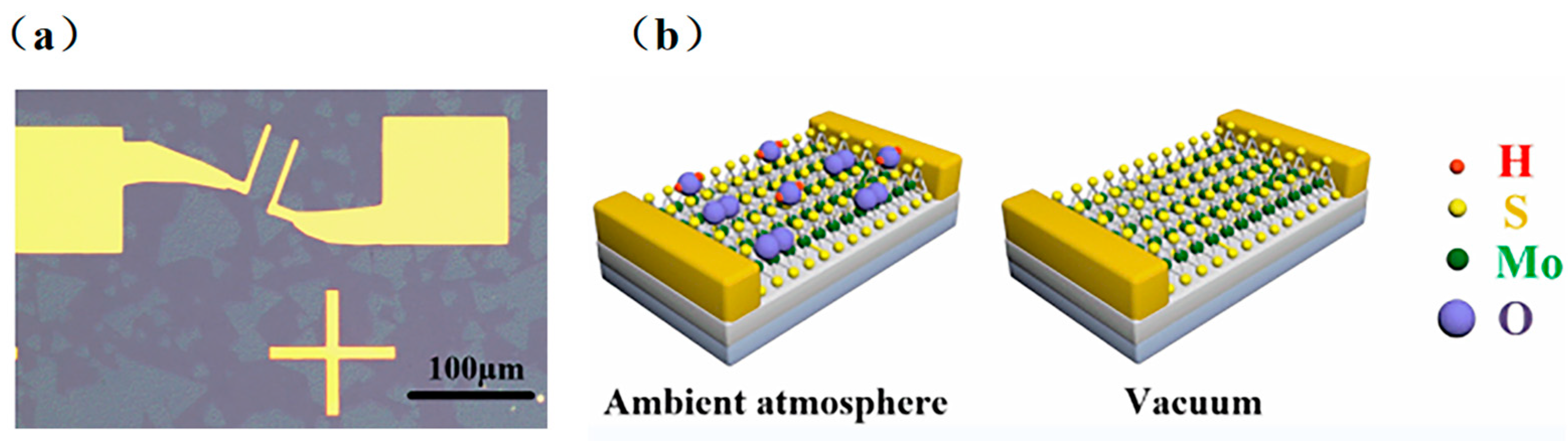
2. Experimental Section

The monolayer MoS2 triangular islands were grown inside a multitemperature-zone tubular furnace. Sulfur powder was placed outside the hot zone and was mildly sublimated with heating belts at 100 °C. MoO3 powder and sapphire (0001) substrates with no pretreatments were placed in the hot center inside the tube furnace. Argon was used as the carrier gas to convey MoO3-x vapor species to the downstream sapphire substrates. The tube was pumped down to a base pressure of 1 Pa and flushed with Ar carrier gas repeatedly to guarantee a favorable growth atmosphere. The as-grown MoS2 film sample was transferred to a heavily P-doped silicon substrate with a 300 nm oxide layer by using a common wet-transfer process. Initially, the polymethylmethacrylate (PMMA) was spin coated on the as-grown MoS2 film sample. The sample was then heated on a hot plate at 100 °C for 3 min to ensure complete curing of the PMMA. Subsequently, the sample was immersed in a potassium hydroxide (KOH) solution to detach the MoS2 layer from the sapphire. The PMMA/MoS2 sample was then cleaned in deionized water and transferred onto a Si/SiO2 substrate. Following this, the sample was dried in an ambient atmosphere for several hours. To complete the wet-transfer process of MoS2, the PMMA layer was removed by warm acetone, followed by rinsing with isopropyl alcohol (IPA) and drying with N2 gas [12]. For the electrical measurement, the back-gate MoS2 FET was placed in the Lakeshore probe station and analysis conducted by the Agilent semiconductor analyzer B5100. The source-drain contact electrode (20 nm Ti//80 nm Au) was fabricated by electron-beam lithography, electron-beam evaporation and a lift-off process. The back gate MoS2 field-effect transistor (FET) with a channel length of 7.7 μm and a channel width of 30 μm was fabricated (seen in the Figure 1a). Figure 1b shows the schematic diagram of the back-gate MoS2 FET.

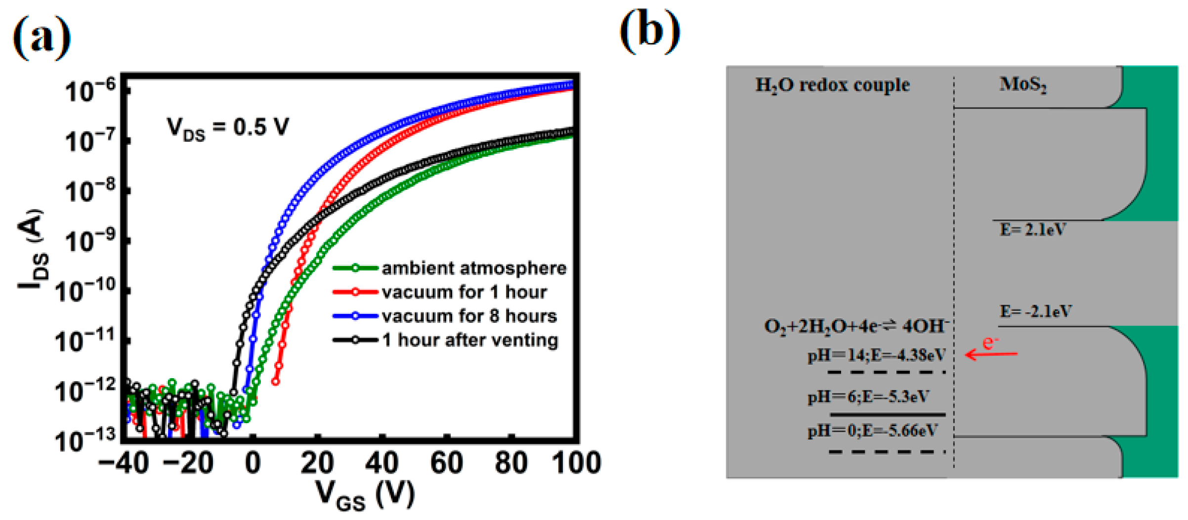
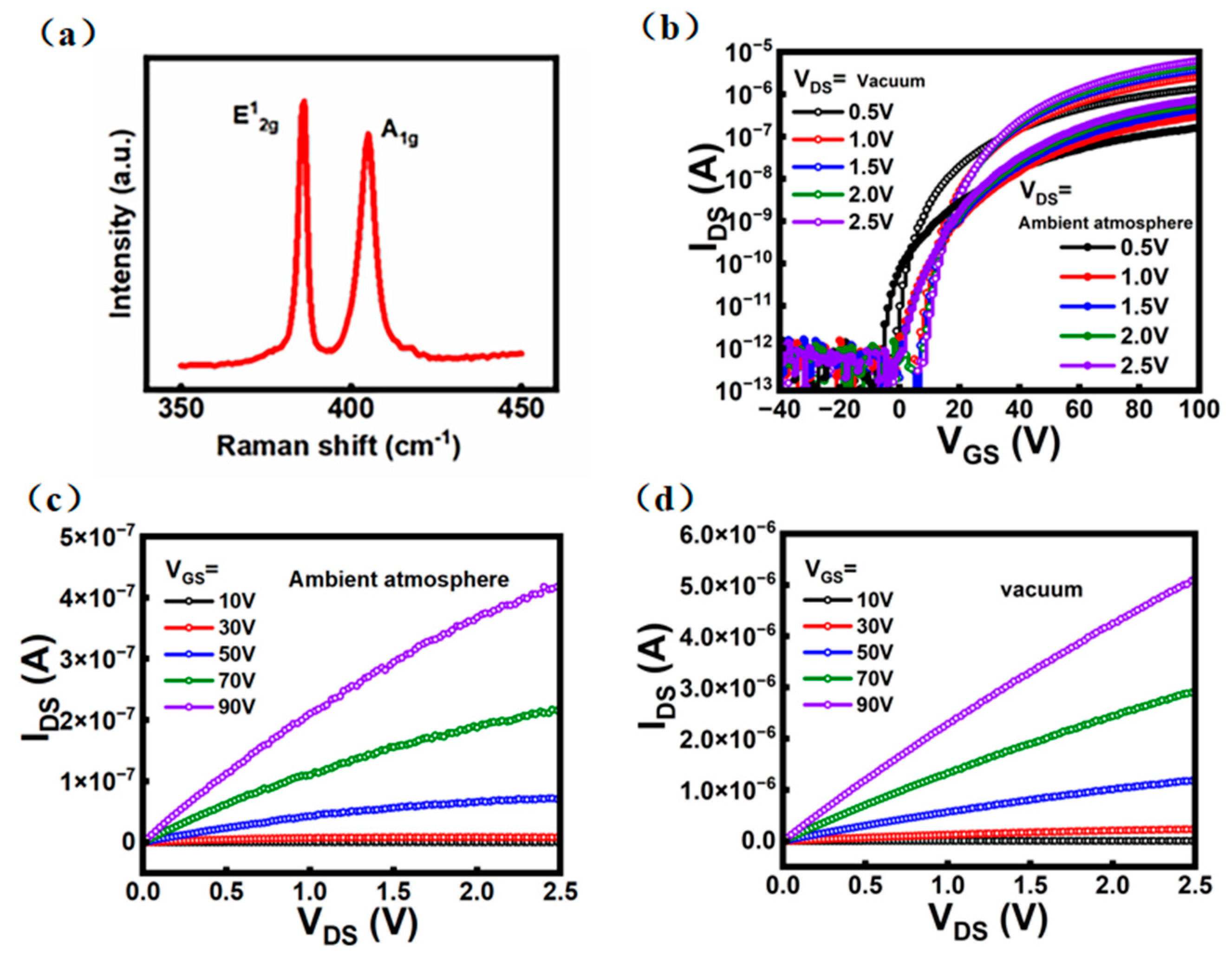
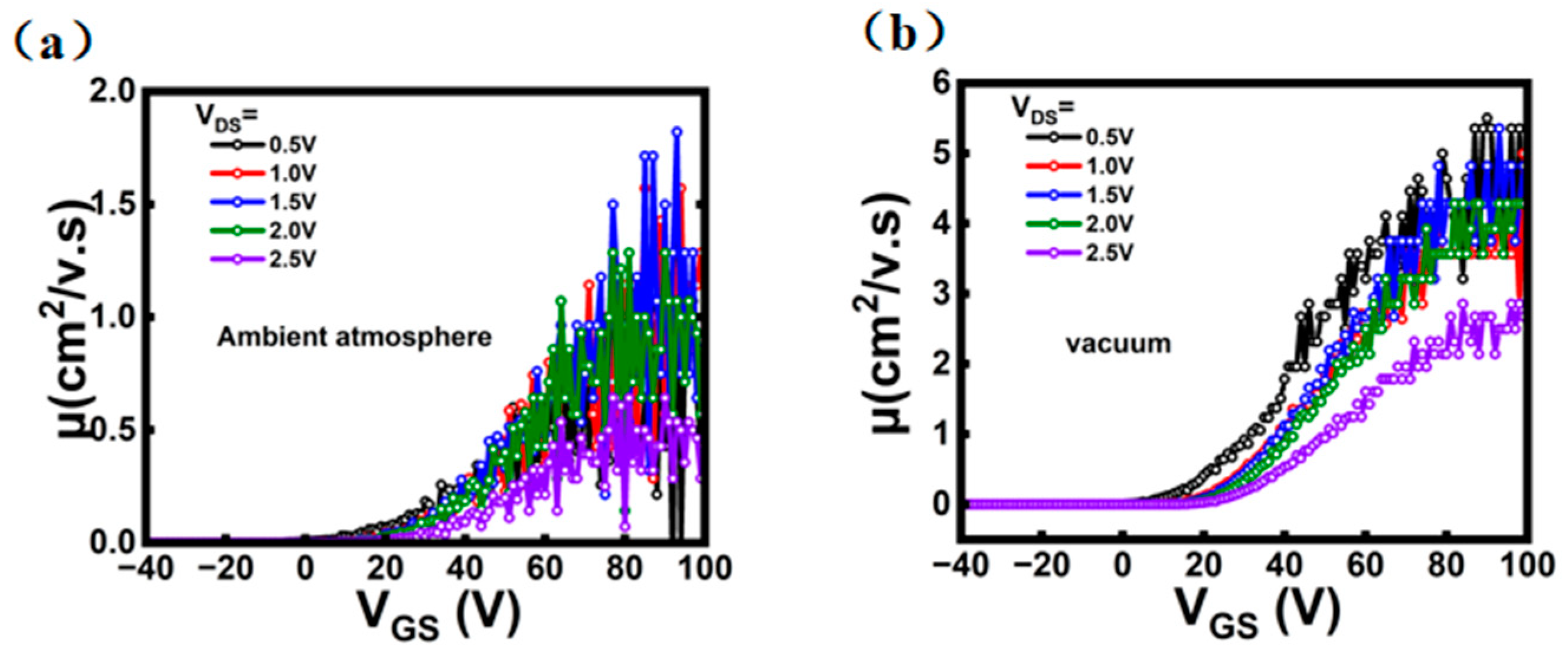
3. Results and Discussion

Firstly, the electrical properties of the back-gate MoS2 FET were measured in an ambient atmosphere. Then, the chamber was evacuated to a vacuum level of 10−6 Torr and kept for eight hours before measuring the back-gate MoS2 FET in a vacuum environment. This extended vacuum process ensures the removal of surface adsorbents induced by the ambient atmosphere. It is important to note that the vacuum pumping process in our study does not involve any heating. However, we acknowledge that heating can be an effective method for desorbing H2O/OH molecules present in the ambient atmosphere. This method may be considered for future studies of the MoS2 FET. Figure 2a shows the transfer characteristic curves of the back-gate MoS2 FET for an ambient atmosphere, kept in a 10−6 Torr vacuum for 1 h, kept in a 10−6 Torr vacuum for 8 h, and 1 h after venting the chamber. The back gate voltage (VGS) sweeps from −40 V to 100 V. The source to drain voltage (VDS) is fixed at 0.5 V. The on current of the back-gate MoS2 FET increases from 1.45 × 10⁻⁷ A to 1.27 × 10⁻⁶ A, after pumping the vacuum down to 10−6 Torr from the ambient atmosphere and maintaining this for 1 h. Furthermore, it increases to 1.36 × 10⁻⁶ A after maintaining 10−6 Torr for 8 h. When the chamber is vented and kept in an ambient atmosphere for 1 h, the on current of the back-gate MoS2 FET decreases to 1.6 × 10⁻⁷ A, but it is still higher than that in an initial ambient atmosphere.
In an ambient atmosphere, for a back-gated molybdenum disulfide field-effect transistor, there exists an adsorbed water layer with dissolved oxygen on the SiO2 surface, which leads to the suppression of electron conduction. This is caused by the electrochemical charge transfer reaction between the semiconductor channel and the dissolved oxygen in water. Charge transfer in the oxygen/water environment is achieved through electron transfer between the semiconductor channel and the oxygen electrochemical oxidation-reduction pair in water. This electron transfer process involves the transfer of electrons from the semiconductor channel to the oxygen in water, forming negatively charged chemical intermediates, subsequently leading to the generation and charging of acceptor states on the substrate surface. This charge transfer process may alter the electronic properties of many organic and inorganic semiconductors in humid air. Therefore, the charge transfer of the oxygen/water oxidation–reduction pair is an important phenomenon in charge transport in the oxygen/water environment.
The aforementioned process is a result of spontaneous electron transfer between a MoS2 and oxygen solvated in water, mediated by the redox reaction [13]:
O 2 + 4 H + + 4 e 2 H 2 O
Figure 2b illustrates the energy level diagram of the water/oxygen redox couple on the left, while on the right it presents the density of states of single-layer MoS2. The chemical potential of this oxygen/water layer is located between −5.66 to −4.83 eV relative to the vacuum level, depending on the pH of the solution (ranging from 0 to 14). Charge transfer will continue to occur before reaching equilibrium, and the Fermi level of the semiconductor will align with the electrochemical potential of the oxygen/water layer. Carla M and others explicitly mention the possibility of electron transfer in two-dimensional materials exposed to moist air. Electrons located at the top of the valence band (−5.66 to −4.83 eV) will easily transfer from the semiconductor molybdenum disulfide to the oxygen/water layer due to their proximity to the adsorbed oxygen’s oxidation–reduction potential on the SiO2 surface [14]. This electrochemical charge transfer process may generate negative chemical intermediates, such as peroxides, which, in turn, can induce charged acceptor states on the substrate surface. It is the electrochemical charge transfer reaction occurring between the dissolved oxygen in the adsorbed water layer on the SiO2 surface and the semiconductor channel that suppresses electron conduction.
Figure 3a shows the Raman spectra of the monolayer MoS2 film excited by a 473 nm laser line at room temperature. The E12g model and A1g was located at 386 and 405, respectively. The E12g model arises from the vibration of an S–Mo–S layer against the adjacent layer. The A1g model is associated with the out-of-plane vibration of only S atoms in opposite directions. The separation of E12g and A1g peaks was found to be 19 cm−1, indicating the single layer nature of the MoS2 film [15]. Figure 3b shows the transfer characteristic of back-gate MoS2 FET in ambient atmosphere. The back-gate voltage (VBG) scans from −40 V to 100 V in 1 V steps. The source-drain voltage (VDS) is swept from 0.5 V to 2.5 V with a step of 0.5 V. The drain current (IDS) increases with the increasing VBG, indicating the n-type transistor behavior. The current on/off ratio is defined as the ratio of the current in the on-state to the current in the off-state for a field-effect transistor (FET). It is a crucial parameter for evaluating the performance of FETs. Enhancing the current on/off ratio has the potential to significantly improve the overall device performance and efficiency. A higher current on/off ratio can effectively reduce the leakage current in the off-state, thereby minimizing power consumption [16]. For the VDS = 2.5 V, the on current (Ion) and off current (Ioff) are observed at 7.4 × 10⁻⁷ A and 5.1 × 10⁻¹³ A, respectively. Additionally, the Ion/Ioff ratio is determined as 1.4 × 10⁶. Then, the chamber vacuum was pumped down to 10−6 Torr and maintained for eight hours before the measurement of back-gate MoS2 FET for the vacuum environment. As a result, the on current of the same back-gate MoS2 FET can be increased to 6.3 × 10⁻⁶ A. Considering the Ioff is 3.5 × 10⁻¹³ A, the Ion/Ioff can be improved to 1.8 × 10⁷. The increasing drain current and on/off ratio can be attributed to the desorption of oxygen and water molecules benefiting from the vacuum environment. In addition, the threshold-voltage shows a positive shift under the vacuum environment, indicating the electronic depletion of n-type MoS2 in an ambient atmosphere. This depletion can be owing to the electron transferred from the two-dimensional semiconductor to the aqueous oxygen redox couple originating from the oxygen/water layer on the MoS2 surface. Figure 3c,d show the output characteristics of the back-gate MoS2 FET in ambient air and vacuum, respectively. The near linear IDS-VDS curve at low bias and observed IDS variation for different values of VBG indicate that the field-effect behavior of our transistor is dominated by the MoS2 channel and not the parasitic resistance [17].
The mobility of charge carriers is a crucial parameter in FETs as it determines their speed of movement in materials under the influence of an electric field. In the case of MoS2 FETs, mobility refers to the rate at which electrons or holes move within the material. Higher mobility indicates that charge carriers can move faster, resulting in improved switching characteristics and increased current flow [18,19]. However, achieving high mobility is not a simple task as there are various factors that can limit the movement of charge carriers. One of the main reasons for low mobility in single-layer MoS2 devices at room temperature is the presence of charge traps between the substrate and the MoS2 layer. When carriers move through semiconductors, they can become trapped by these charge traps. The trapped carriers remain in the traps for a certain duration, leading to a decrease in effective carrier concentration and mobility [20]. Additionally, when the MoS2 layer is exposed to ambient air, molecules of oxygen and water can adsorb onto its surface, resulting in an increase in the number of charge traps. In a vacuum environment, the surface of the MoS2 layer is almost free from impurities, leading to a significant reduction in the density of charge traps. As a result, the mobility of carriers is higher in a vacuum since they are not limited or scattered by charge traps. Consequently, the reduction in charge traps improves the mobility of carriers, which is particularly advantageous for MoS2 FETs as it enhances their performance and efficiency [21,22].
The field effect carrier mobility (µFE) of the back-gate MoS2 FET can be extracted from the following expression:
μ F E = L g m W C o x V D S
where gm is the transconductance that can be determined by d(IDS)/d(VBG), Cox is the back-gate capacitance per unit area, L is the gate length and W is gate width. The value of Cox can be estimated to be 11.50 nF/cm−2 through using the equation, Cox = κε0/tox, where κ is the SiO2 relative dielectric constant with value of 3.9 and ε0 is the permittivity of free space. The Keithley 4200 semiconductor parameter analyzer was used to measure the back-gate MoS2 FET in a non-vacuum and vacuum environment.
The µFE of the back-gate MoS2 FET derived from gm in ambient air and vacuum are shown in Figure 4a,b, respectively. After the vacuum pumping process, the values of µFE can be increased by more than four times, from about 1 cm2/Vs to about 4.2 cm2/Vs. This obviously enhanced µFE is explained below. When the MoS2 layer is exposed to the ambient air, the oxygen and water molecules will be absorbed on the MoS2 surface, especially on defects and edges. The vacancies in the plane and edges of MoS2 have high catalytic activity for oxygen and water chemisorption at room temperature, which could act as extra Coulomb scatters for electrons. After the vacuum process, the weakened scattering induced by partial oxygen and water molecules’ desorption will lead to the promotion of the carrier mobility [23].
The application of high mobility MoS2 FET in a large area of integrated circuits holds significant importance. MoS2 FET exhibit excellent electron transport performance, enabling high-speed and low-power operation, thereby enhancing the efficiency and performance of integrated circuits. The high mobility of MoS2 FET also presents promising prospects in the field of biosensors and flexible electronic devices. In the realm of biosensors, MoS2 FET with high mobility can serve as sensitive detectors for biochemical substances. These transistors can convert chemical signals into electrical signals, facilitating the sensitive detection of biomolecules. Such biosensors hold great potential for applications in medical diagnosis, environmental monitoring, and food safety, playing a crucial role in these areas [24]. Furthermore, a MoS2 FET with high mobility can find applications in high-speed electronic devices. For instance, in high-frequency amplifiers and communication systems, MoS2 FETs can exhibit fast switching characteristics and response speeds, enabling high-frequency operation and reduced switching delays. This makes them highly suitable for such applications. MoS2 FET with high mobility also offer potential applications in flexible electronic devices. Their thin film structure and high mobility allow them to maintain their performance even under bending and stretching conditions, making them suitable for wearable devices, flexible display screens, and other related fields. These flexible electronic devices provide a more comfortable and portable user experience and have broad application prospects. High mobility plays a critical role in MoS2 FETs. By increasing the mobility, the speed of electron movement within the transistor can be enhanced, leading to improved response speed and working frequency [25]. Additionally, high mobility reduces scattering losses, resulting in reduced energy consumption and heat generation, thus enabling low-power operation. Consequently, increasing mobility enhances the performance and efficiency of MoS2 FET. By focusing on enhancing the mobility of MoS2 FET, researchers and engineers can unlock their full potential in various applications, ranging from integrated circuits to biosensors and flexible electronic devices. This will contribute to advancements in technology and pave the way for future innovation in these fields.
SS refers to the relationship between the input voltage and the output current when a field effect transistor (FET) operates in the sub-threshold region, which is below the threshold voltage. It is a crucial parameter for assessing the performance of low-power electronic devices and integrated circuits. In the sub-threshold region, the switching characteristics and energy consumption of the FET are influenced by the sub-threshold swing. A smaller SS indicates that the FET can effectively control the output current with minimal input voltage variation, thereby reducing power consumption. However, when considering the MoS2–SiO2 interface and other material interfaces, the presence of interface states significantly impacts the performance and stability of MoS2 FETs, particularly the stability of the SS. Interface states refer to defects or impurities formed at the material interface. These interface states increase the SS, leading to slower switching speeds and higher static power consumption. Thus, investigating the formation and control of interface states is crucial for optimizing the performance of MoS2 FETs. In a vacuum environment, the formation of interface states is reduced due to the absence of gas molecule adsorption. This reduction in interface states leads to a decrease in the SS of MoS2 FETs. The utilization of a vacuum environment effectively mitigates the adverse effects of interface states on the performance of MoS2 FETs. Furthermore, the vacuum environment also reduces impurity diffusion and surface oxidation, further minimizing the number of interface states and subsequently reducing the SS. Therefore, a vacuum environment can be considered as a favorable condition for enhancing the performance of MoS2 FETs [26,27].
The subthreshold swing (SS) of a MoS2–SiO2 interface is affected by the density of interface states (Dit). The presence of interface states causes an elevation in the subthreshold swing, resulting in a decrease in switching speed and an increase in static power consumption. The relationship between SS and density can be described by the following equations:
S S = l n 10 × k T q × 1 + C i t C O X
D i t = C i t / q 2
where k is the Boltzmann’s constant, T is the measurement temperature, q is the electron charge, and Cox is the gate dielectric capacitance density which is 11.5 nF/cm2 (Cox = ε0εr/d; εr = 3.9; d = 300 nm) for the MoS2 FET.
In the vacuum state, the presence of interface states on the surface of a MoS2 FET is diminished, resulting in a decrease in interface state density. This phenomenon can be attributed to the interaction between interface states and the vacuum environment. In a vacuum, the formation of interface states is less influenced by the surrounding environment, leading to a reduction in their density. The decrease in interface state density has a positive impact on the performance of the MoS2 FET. It mitigates the influence of interface traps on electron transport, thereby reducing the subthreshold swing. Consequently, the transistor exhibits enhanced sensitivity and linearity in current variation at low voltages, thereby improving its switching characteristics and current amplification ability [28]. Hence, the values of SS can be obtained from the transfer characteristics in Figure 3, according to the equation:
  S S   =   V B G l g I D S
Figure 5 shows the values of SS as a function of IDS for the back-gate MoS2 FET in ambient air and a vacuum, respectively. In the IDS range of 10−13 A to 10−6 A, the value of SS increases with the increasing IDS and decreases with the increasing VDS. The minimum value of SS for the back-gate MoS2 FET in ambient air is 400 mV/dec. However, it decreases by 30%, down to 280 mV/dec after the vacuum process. The decrease in SS can be attributed to the less interfacial states beneficiating from the partial desorption of oxygen and water molecules.
In the field of low-power electronic devices, as electronic devices become smaller and the demand for power consumption decreases, reducing the sub-threshold swing has become an important technical method. The reduction in sub-threshold swing can be achieved by reducing the threshold voltage of the transistor. When the threshold voltage of the transistor is reduced to the sub-threshold level, the current change in the transistor will be more sensitive and linear, thereby enabling the transistor to exhibit stable operating characteristics even at low voltage. This characteristic is very advantageous for the design of low-power electronic devices because it can achieve higher switching efficiency and lower power consumption at lower voltage. In addition, reducing sub-threshold swing can also effectively reduce the leakage current of the transistor, thereby improving the reliability and long-term stability of the device. Therefore, the technique of reducing sub-threshold swing has become an indispensable part of the design of low-power electronic devices, with broad application prospects and research value [29]. Similarly, in high-frequency electronic devices, fast switching characteristics and response speed are crucial. By reducing the subthreshold swing, MoS2 FETs can potentially achieve higher operating frequencies and shorter switch delays. This makes them suitable for high-frequency electronic devices such as RF amplifiers and communication systems. Moreover, the reduction in subthreshold swing can enhance the sensitivity and accuracy of sensors [30]. By decreasing the interface state density in a vacuum environment, MoS2 FETs may possess higher signal detection capabilities. This opens up possibilities for their application in various sensors, including optical sensors, chemical sensors, and biological sensors. In conclusion, the study and application of MoS2 FETs in a vacuum environment hold promise for improved performance and applications in fields such as low-power electronic devices, high-frequency electronic devices, and sensor technology [31,32].

4. Conclusions

In this study, we demonstrated the efficacy of vacuum treatment in preserving the electrical characteristics of back-gate MoS2 FETs. Through the meticulous removal of oxygen and water molecules from the surface of MoS2, we have achieved a substantial improvement in device performance [33]. Specifically, we report a remarkable increase in the switching ratio of back-gate MoS2 devices, elevating it from 1.4 × 10⁶ to an impressive 1.8 × 10⁷. Moreover, we have observed a significant enhancement in the field effect carrier mobility, soaring from approximately 1 cm2/Vs to an impressive 4.2 cm2/Vs. Meanwhile, we identified a 30% decrease in the sub-threshold swing value when compared to measurements made in ambient air. Overall, this study provides a theoretical and experimental basis for reducing the interfacial adsorption effect of MoS2 devices in the future. It was demonstrated that by optimizing the performance of MoS2 field effect transistors in vacuum environments, device degradation and instability are addressed and device performance and efficiency are improved [34].

Author Contributions

Conceptualization, J.L. and S.P.; validation, J.L., S.P. and Z.J.; formal analysis, J.L., S.P. and H.T.; investigation, J.L., X.P., T.W. and S.P. resources, S.P.; data curation, J.L. and S.P.; writing—original draft preparation, S.P.; writing—review and editing, J.L., S.P. and Z.J.; visualization, J.L. supervision, S.P. and H.T.; project administration, S.P.; funding acquisition, S.P. All authors have read and agreed to the published version of the manuscript.

Funding

STI 2030—Major Projects (2022 ZD0209200), Youth Innovation Promotion Association of Chinese Academy of Sciences (2019120), and the opening fund of Key Laboratory of Science and Technology on Silicon Devices, Chinese Academy of Sciences.

Institutional Review Board Statement

Not applicable.

Informed Consent Statement

Not applicable.

Data Availability Statement

All data that support the findings of this study are included within the article.

Conflicts of Interest

The authors declare no conflict of interest.

References

  1. Jiang, J.; Ahyi, A.C.; Dhar, S. Dual-gate MoS2 FET with a coplanar-gate engineering. IEEE Trans. Electron Devices 2015, 63, 573–577. [Google Scholar] [CrossRef]
  2. Pan, Y.; Jia, K.; Huang, K.; Wu, Z.; Bai, G.; Yu, J.; Zhang, Z.; Zhang, Q.; Yin, H. Near-ideal subthreshold swing MoS2 back-gate transistors with an optimized ultrathin HfO2 dielectric layer. Nanotechnology 2019, 30, 96–98. [Google Scholar] [CrossRef] [PubMed]
  3. Lee, K.M.; Oh, Y.; Yoon, H.; Chang, M.; Kim, H. Multifunctional role of MoS2 in preparation of composite hydrogels: Radical initiation and cross-linking. ACS Appl. Mater. Interfaces 2020, 12, 8642–8649. [Google Scholar] [CrossRef] [PubMed]
  4. Radisavljevic, B.; Whitwick, M.B.; Kis, A. Integrated circuits and logic operations based on single-layer MoS2. ACS Nano 2011, 5, 9934–9938. [Google Scholar] [CrossRef]
  5. Bagsican, F.R.; Winchester, A.; Ghosh, S.; Zhang, X.; Ma, L.; Wang, M.; Murakami, H.; Talapatra, S.; Vajtai, R.; Ajayan, P.M.; et al. Adsorption energy of oxygen molecules on graphene and two-dimensional tungsten disulfide. Sci. Rep. 2017, 7, 1774–1779. [Google Scholar] [CrossRef]
  6. Tongay, S.; Zhou, J.; Ataca, C.; Liu, J.; Kang, J.S.; Matthews, T.S.; You, L.; Li, J.; Grossman, J.C.; Wu, J. Broad-range modulation of light emission in two-dimensional semiconductors by molecular physisorption gating. Nano Lett. 2013, 13, 2831–2836. [Google Scholar] [CrossRef]
  7. Wang, X.F.; Tian, H.; Liu, Y.; Shen, S.; Yan, Z.; Deng, N.; Yang, Y.; Ren, T.-L. Two-mode MoS2 filament transistor with extremely low subthreshold swing and record high on/off ratio. ACS Nano 2019, 13, 2205–2212. [Google Scholar] [CrossRef]
  8. Alexandrou, K.; Farmakis, F.; Arapis, A.; Georgoulas, N.; Hao, Y.; Hone, J.; Kymissis, I. Effect of vacuum thermal annealing to encapsulated graphene field effect transistors. J. Vac. Sci. Technol. B 2016, 34, 171–177. [Google Scholar] [CrossRef]
  9. English, C.D.; Shine, G.; Dorgan, V.E.; Saraswat, K.C.; Pop, E. Improved contacts to MoS2 transistors by ultra-high vacuum metal deposition. Nano Lett. 2016, 16, 3824–3830. [Google Scholar] [CrossRef]
  10. Nan, H.; Wang, Z.; Wang, W.; Liang, Z.; Lu, Y.; Chen, Q.; He, D.; Tan, P.; Miao, F.; Wang, X.; et al. Strong photoluminescence enhancement of MoS2 through defect engineering and oxygen bonding. ACS Nano 2014, 8, 5738–5745. [Google Scholar] [CrossRef]
  11. Sun, L.; Zhang, X.; Liu, F.; Shen, Y.; Fan, X.; Zheng, S.; Thong, J.T.L.; Liu, Z.; Yang, S.A.; Yang, H.Y. Vacuum level dependent photoluminescence in chemical vapor deposition-grown monolayer MoS2. Sci. Rep. 2017, 7, 16714. [Google Scholar] [CrossRef] [PubMed]
  12. Wang, X.; Kang, K.; Chen, S.; Du, R.; Yang, E.-H. Location-specific growth and transfer of arrayed MoS2 monolayers with controllable size. 2D Mater. 2017, 4, 025093. [Google Scholar] [CrossRef]
  13. Aguirre, C.M.; Levesque, P.L.; Paillet, M.; Lapointe, F.; St-Antoine, B.C.; Desjardins, P.; Martel, R. The role of the oxygen/water redox couple in suppressing electron conduction in field-effect transistors. APS March Meet. Abstr. 2009, 17, 24–32. [Google Scholar] [CrossRef]
  14. Chua, L.-L.; Zaumseil, J.; Chang, J.-F.; Ou, E.C.-W.; Ho, P.K.-H.; Sirringhaus, H.; Friend, R.H. General observation of n-type field-effect behaviour in organic semiconductors. Nature 2005, 434, 194–199. [Google Scholar] [CrossRef] [PubMed]
  15. Chakraborty, B.; Matte, H.S.S.R.; Sood, A.K.; Rao, C.N.R. Layer-dependent resonant Raman scattering of a few layer MoS2. J. Raman Spectrosc. 2013, 44, 92–96. [Google Scholar] [CrossRef]
  16. Qiu, H.; Pan, L.; Yao, Z.; Li, J.; Shi, Y.; Wang, X. Electrical characterization of back-gated bi-layer MoS2 field-effect transistors and the effect of ambient on their performances. Appl. Phys. Lett. 2012, 100, 2024–2027. [Google Scholar] [CrossRef]
  17. Cho, K.; Park, W.; Park, J.; Jeong, H.; Jang, J.; Kim, T.-Y.; Hong, W.-K.; Hong, S.; Lee, T. Electric stress-induced threshold voltage instability of multilayer MoS2 field effect transistors. ACS Nano 2013, 7, 7751–7758. [Google Scholar] [CrossRef]
  18. Iqbal, M.W.; Elahi, E.; Amin, A.; Aftab, S.; Aslam, I.; Hussain, G.; Shehzad, M.A. A facile route to enhance the mobility of MoTe2 field effect transistor via chemical doping. Superlattices Microstruct. 2020, 147, 106–114. [Google Scholar] [CrossRef]
  19. Yu, Z.; Ong, Z.-Y.; Li, S.; Xu, J.-B.; Zhang, G.; Zhang, Y.-W.; Shi, Y.; Wang, X. Analyzing the carrier mobility in transition-metal dichalcogenide MoS2 field-effect transistors. Adv. Funct. Mater. 2017, 27, 160–172. [Google Scholar] [CrossRef]
  20. Radisavljevic, B.; Kis, A. Mobility engineering and a metal–insulator transition in monolayer MoS2. Nat. Mater. 2013, 12, 815–820. [Google Scholar] [CrossRef]
  21. Kim, J.H.; Lee, J.; Kim, J.H.; Hwang, C.C.; Lee, C.; Park, J.Y. Work function variation of MoS2 atomic layers grown with chemical vapor deposition: The effects of thickness and the adsorption of water/oxygen molecules. Appl. Phys. Lett. 2015, 106, 1230–1238. [Google Scholar] [CrossRef]
  22. Qi, L.; Wang, Y.; Shen, L.; Wu, Y. Chemisorption-induced n-doping of MoS2 by oxygen. Appl. Phys. Lett. 2016, 108, 30–36. [Google Scholar] [CrossRef]
  23. Jiang, J.; Zhang, Y.; Wang, A.; Duan, J.; Ji, H.; Pang, J.; Sang, Y.; Feng, X.; Liu, H.; Han, L. Construction of high field-effect mobility multilayer MoS2 field-effect transistors with excellent stability through interface engineering. ACS Appl. Electron. Mater. 2020, 2, 2132–2140. [Google Scholar] [CrossRef]
  24. Majd, S.M.; Salimi, A.; Ghasemi, F. An ultrasensitive detection of miRNA-155 in breast cancer via direct hybridization assay using two-dimensional molybdenum disulfide field-effect transistor biosensor. Biosens. Bioelectron. 2018, 105, 6–13. [Google Scholar] [CrossRef]
  25. Singh, E.; Singh, P.; Kim, K.S.; Yeom, G.Y.; Nalwa, H.S. Flexible molybdenum disulfide (MoS2) atomic layers for wearable electronics and optoelectronics. ACS Appl. Mater. Interfaces 2019, 11, 11061–11105. [Google Scholar] [CrossRef]
  26. Huang, X.; Yao, Y.; Peng, S.; Zhang, D.; Shi, J.; Jin, Z. Effects of charge trapping at the MoS2–SiO2 interface on the stability of subthreshold swing of MoS2 field effect transistors. Materials 2020, 13, 2896. [Google Scholar] [CrossRef]
  27. Trung, N.T.; Hossain, M.I.; Alam, I.; Ando, A.; Kitakami, O.; Kikuchi, N.; Takaoka, T.; Sainoo, Y.; Arafune, R.; Komeda, T. In Situ Study of Molecular Doping of Chlorine on MoS2 Field Effect Transistor Device in Ultrahigh Vacuum Conditions. ACS Omega 2020, 5, 28108–28115. [Google Scholar] [CrossRef]
  28. Liu, X.; Liang, R.; Gao, G.; Pan, C.; Jiang, C.; Xu, Q.; Luo, J.; Zou, X.; Yang, Z.; Liao, L.; et al. MoS2 Negative-Capacitance Field-Effect Transistors with Subthreshold Swing below the Physics Limit. Adv. Mater. 2018, 30, 180–186. [Google Scholar] [CrossRef]
  29. Oh, G.H.; An, J.G.; Kim, S.-I.; Shin, J.C.; Park, J.; Kim, T.W. Ultralow Subthreshold Swing 2D/2D Heterostructure Tunneling Field-Effect Transistor with Ion-Gel Gate Dielectrics. ACS Appl. Electron. Mater. 2022, 5, 196–204. [Google Scholar] [CrossRef]
  30. Kaushal, P.; Khanna, G. MoS2 based Thickness Engineered Tunnel field-effect transistors for RF/analog applications. Mater. Sci. Semicond. Process. 2022, 151, 107016. [Google Scholar] [CrossRef]
  31. Tao, X.; Liu, L.; Xu, J. Improved Subthreshold Swing of MoS2 Negative-Capacitance Transistor by Using HfZrAlO as Ferroelectric Layer of Gate-Stack. IEEE Trans. Electron Devices 2022, 70, 796–800. [Google Scholar] [CrossRef]
  32. Liu, Y.; Li, Q.-X.; Zhu, H.; Ji, L.; Sun, Q.-Q.; Zhang, D.W.; Chen, L. Dual-gate manipulation of a HfZrOx-based MoS2 field-effect transistor towards enhanced neural network applications. Nanoscale 2023, 15, 313–320. [Google Scholar] [CrossRef] [PubMed]
  33. McMorrow, J.J.; Cress, C.D.; Arnold, H.N.; Sangwan, V.K.; Jariwala, D.; Schmucker, S.W.; Marks, T.J.; Hersam, M.C. Vacuum ultraviolet radiation effects on two-dimensional MoS2 field-effect transistors. Appl. Phys. Lett. 2017, 110, 84–90. [Google Scholar] [CrossRef]
  34. Li, T.; Du, G.; Zhang, B.; Zeng, Z. Scaling behavior of hysteresis in multilayer MoS2 field effect transistors. Appl. Phys. Lett. 2014, 105, 5216–5228. [Google Scholar] [CrossRef]
Figure 1. (a) Optical image of the back-gate MoS2 field effect transistor; (b) Schematic diagram of the back-gate MoS2 field effect transistor.
Crystals 13 01501 g001
Figure 2. (a) Transfer characteristic curves of MoS2 field effect transistor in an ambient atmosphere, kept at a 10−6 Torr vacuum for 1 h, kept at a 10−6 Torr vacuum for 8 h, and 1 h after venting the chamber. (b) Energy level diagram of the water/oxygen redox couple (left) compared to the density of states of single-layer MoS2 (right). The arrow indicates the direction of the charge transfer reaction.
Crystals 13 01501 g002
Figure 3. (a) Raman spectra of the monolayer of MoS2. (b) Transfer characteristic curve of MoS2 field effect transistor in an ambient atmosphere and under vacuum. (c) Output characteristic curve of the MoS2 field effect transistor in an ambient atmosphere. (d) Output characteristic curve of the MoS2 field effect transistor in a vacuum.
Crystals 13 01501 g003
Figure 4. (a) The field-effect carrier mobility of the MoS2 field effect transistor as a function of back-gate voltage in an ambient atmosphere. (b) The field-effect carrier mobility of the MoS2 field effect transistor as a function of back-gate voltage in a vacuum.
Crystals 13 01501 g004
Figure 5. Comparison of the sub-threshold swing as a function of source-drain current for the back-gate MoS2 FET in ambient air and a vacuum.
Crystals 13 01501 g005
Disclaimer/Publisher’s Note: The statements, opinions and data contained in all publications are solely those of the individual author(s) and contributor(s) and not of MDPI and/or the editor(s). MDPI and/or the editor(s) disclaim responsibility for any injury to people or property resulting from any ideas, methods, instructions or products referred to in the content.

