Article

Phase Field Simulation Research on the Microstructural Evolution of Monocrystalline and Polycrystalline Silicon

1
College of Physics and Electronic Science, Anshun University, Anshun 561000, China
2
School of Materials Science and Engineering, Qingdao University, Qingdao 266071, China
*
Author to whom correspondence should be addressed.
Crystals 2022, 12(9), 1271; https://doi.org/10.3390/cryst12091271
Submission received: 14 August 2022 / Revised: 29 August 2022 / Accepted: 30 August 2022 / Published: 7 September 2022

Abstract

:
This work simulates the morphological evolution process of the solidification interface of silicon crystal. Based on the phase field model of single dendrite growth of pure material in a single-phase system, the control equation of the phase field is re-optimized, and an interface free energy anisotropy equation that can simulate the competitive growth of multiple crystal grains is established. The competitive growth of polysilicon is then simulated and analyzed. The results show that when the degree of undercooling exceeds a certain value, the non-facet crystals are transformed into facet crystals. The main branches in each direction are relatively thick when the anisotropy is small. With increasing anisotropy, the main branches in each direction show gradual thinning, and edges and corners appear on the interface. The dendrites are no longer smooth, and they transform from non-facet crystals to facet crystals. The main branches of different grains inhibit each other when multiple crystal grains compete for growth. The growth of the main branches is curved, which is different from existing branches. The experimental results can more realistically simulate the evolution process of single-crystal silicon and polycrystalline silicon crystal micromorphology.

1. Introduction

Photovoltaics are an important renewable energy source [1]. Since the first solar cell was developed by Bell Labs in 1954, photoelectric conversion has been an effective way to solve energy and environmental problems [2]. The silicon material itself has obvious anisotropy and low-phase transition entropy is more suitable for facet growth. The growth of dendrites requires a large degree of supercooling, and accurate control of the degree of supercooling can produce quasi-single crystals, which can impede the industrial production of silicon quasi-single crystals [3].
Fujiwara et al. [4,5] reported the growth of polycrystalline silicon grains. Dendrite induction in the initial nucleation stage turned to large-grained polycrystalline silicon with a specific crystal orientation; its photovoltaic conversion efficiency was close to that of single-crystalline silicon solar cells. Nagashio et al. [6] confirmed that the typical dendrite growth directions are <211>, <110>, and <100>. The growth direction and shape of facet dendrites are different with increases in undercooling. Thus, the crystallographic orientation can be controlled by controlling the degree of supercooling. The size and orientation of the grain dramatically affect the minority carrier lifetime, thus, it is critical to control the grain growth (especially grain competition) for the conversion efficiency improvement [4,5,6,7].
T. Aoyama et al. [7] obtained a silicon dendrite morphology via large supercooling experiments. The growth of Si was classified into the three categories of lateral growth, isolated dendrite growth, and close dendrite growth at low, moderate, and high undercooling values, respectively. The first transition in the classification was caused by a change into three categories: lateral growth, isolated, and high undercooling values. However, there is no such simulation showing the key experimental features so far. P. Chen’s [8] results agree well with experimental observations.
The phase field method uses continuous variables to simulate discontinuous phenomena. The simple algorithm and powerful functions make it popular. The phase field method can couple the nucleation model, the growth model, and the influencing factors in the growth process with the basic heat transfer equation for more accurate microscopic numerical simulations. Phase field simulations will continue to expand studies on material microstructure evolution. Phase field modeling can analyze facet crystal growth, which is powerful for describing the growing interface morphology, and many studies have illustrated the power of such models [9,10]. Based on considered the phenomena of nucleation, Granasy et al. [11,12,13,14] have successfully modeled the solidification of highly anisotropic systems. Lin et al. [15] simulated the 3D phase field of directionally solidified silicon film growth. Kasajima et al. [16] applied the small solid/liquid interface limit to the phase field model to simulate the growth of small crystal face dendrites during solidification of supercooled Si. The simulation results were similar to the Gibbs–Thomson relationship. Suzuki [17] used the phase field method to simulate the growth of two-dimensional Si facet dendrites in supercooled Si-Ni alloys. The results show a relationship between the size of the dendrite tip and the growth rate. Chen et al. [18] used the phase field method to simulate and calculate the evolution process of the dendrites on a facet of elemental silicon to obtain the influence law of the anisotropy coefficient on dendrite growth. Liu et al. [19] used a phase field model with high interfacial energy anisotropy to study the effect of interfacial energy anisotropy and undercooling on the interface morphology during free growth of silicon grains. Facet grain morphology was seen with edges and corners consistent with the experiment. Yuan et al. [20] simulated the evolution of interface morphology during polysilicon solidification by the phase field method and analyzed the effects of initial nucleation conditions, disturbance intensity, and time step on the interface morphology evolution. However, there are relatively few studies on the subsequent growth stages of large-grained polycrystalline silicon, especially using phase field methods to simulate the preferred direction and competitive growth of polycrystalline silicon.
In this paper, the morphological evolution process of the solidification interface of silicon crystals is simulated, and the evolution mechanism of the silicon crystal microstructure and the influence of phase field parameters on evolution dynamics are discussed in depth through simulation experiments at multiple levels. The control equation of the phase field was re-optimized based on the phase field model of single dendrite growth of pure material in a single-phase system. The interface free energy anisotropy equation could simulate the competitive growth of multiple crystal grains, and the competitive growth of polysilicon was subjected to simulation analysis. The purpose is to have certain guiding significance for production through quantitative simulation.

2. Phase Field Model

In the case of pure matter, a heat diffusion equation is also incorporated along with a latent heat term:
T t = D T 2 T + h ` ( ϕ ) L c p ϕ t
where
D T = K T / c p is the thermal diffusivity, L is the latent heat, and cp is the specific heat capacity. On introducing the dimensionless temperature μ = ( T T M ) ( L / c p ) , (1) takes the following form:
u t = D T 2 u + 1 2 φ t
Consider the anisotropic phase field governing equation:
τ 0 a s ( θ ) φ t = [ φ λ u ( 1 φ 2 ) ] ( 1 φ 2 ) + ε 0 2 ( a s ( θ ) 2 φ ) x ( ε 0 2 a s ( θ ) a s ( θ ) y ) + y ( ε 0 2 a s ( θ ) a s ( θ ) x )
These are Wulff equilibrium crystal shapes [18] at various anisotropy values. When
γ < 1/15, the crystal shape is smooth and continuous. When γ > 1/15, there are discontinuous and concave features similar to “ears”. These “ears” parts increase with increasing anisotropy value. To simulate dendrite growth with strong anisotropy, these “ears” must be removed. The interface energy within the missing orientations has been regularized by Eggleston and Kim as follows:
W ^ ( φ ) = { W ( φ ) , ( π 2 i + φ m ) | φ | π 2 ( i + 1 ) φ m W ( φ m ) cos φ cos φ m , ( π 2 i φ m ) < φ < ( π 2 i + φ m )
where i = 0–3, φ m is the corner angle of the equilibrium shape or the first missing orientation calculated as follows:
W ( φ m ) sin φ m + W φ ( φ m ) cos φ m = 0
( π 2 i + φ m ) φ ( π 2 ( i + 1 ) φ m ) ( i = 0 , 1 , 2 , 3 )
τ ( n ) ϕ t = ( W ( n ) 2 ϕ ) x [ W ( n ) W φ ( n ) y ϕ ] + y [ W ( n ) W φ ( n ) y ϕ ] + ϕ ϕ 3 λ θ ( 1 ϕ 2 ) 2
( π 2 i φ m ) < φ < ( π 2 i + φ m ) ( i = 0 , 2 )
τ ( φ m ) ( cos φ cos φ m ) 2 ϕ t = τ 0 ( W ( φ m ) cos φ m ) 2 ϕ x x + ϕ ϕ 3 λ θ ( 1 ϕ 2 ) 2
( π 2 i φ m ) < φ < ( π 2 i + φ m ) ( i = 1 , 3 )
τ ( φ m ) ( sin φ cos φ m ) ϕ t = τ 0 ( W ( φ m ) cos φ m ) 2 ϕ y y + ϕ ϕ 3 λ θ ( 1 ϕ 2 ) 2
The growth morphology of crystals in supercooled melts is not only related to the crystal growth mechanism but also has an important relationship with the solidification interface structure. The interface free energy has an important influence on the interface structure. For weakly anisotropic crystals, the interface free energy in the diffusion interface region can be expressed as follows:
τ ( n ) = τ 0 ( 1 + ε cos k θ i ) 2
w ( n ) = w 0 ( 1 + ε cos k θ i )
where k is the anisotropy modulus, usually taken as 4, ε is the anisotropy coefficient, θ i is the angle between the preferred growth direction of a certain grain, w 0 is the length range parameter, and τ 0 is the time length range, and this paper takes 1.
θ i = f ( η i ) + θ
where the subscript i represents a certain grain, ϕ y and ϕ x represent the partial derivatives of the phase field in the x-axis and y-axis directions, respectively, and θ = arctan ( φ y / φ x ) represents the angle between the interface normal and the crystal growth principal axis.
f ( η i ) = r i π / 2 ( i = 1 , 2 , , n )
where n represents the number of crystal grains and γ i is a random number between 0 and 1. ϕ represents the phase field parameter; ϕ = 1 in the bulk solid phase and ϕ = −1 in the bulk liquid phase, and the phase field varies smoothly between these two values within the diffusion interface region, where λ = 6.359 [17].

3. Determination and Simulation Calculation of Phase Field Parameters

3.1. Initial and Boundary Conditions

The coordinates of the crystal nuclei in the calculation grid are randomly given, therefore, the crystal nuclei are randomly distributed in the simulation area. The number of crystal grains is any number less than the maximum number of nuclei. The maximum number of nucleation can be calculated from the nucleation density, assuming that the variation in the nucleation density in the model satisfies a Gaussian distribution [21], and is given by
d n d ( Δ T ) = n max 2 Δ T σ exp ( ( Δ T Δ T max ) 2 2 Δ T σ 2 )
where Δ T m a x is the maximum nucleation undercooling, Δ T σ is the standard deviation of the undercooling degree, and n max is the maximum nucleation density.
x 2 + y 2 R 2 ,   ψ = 1 ,   u = 0 ,   V x = 0 ,   p = 0 ;
x 2 + y 2 > R 2 ,   ψ = 1 ,   u = Δ ,   V x = 0 ,   p = 0 ,
where x and y are the abscissa and ordinate, respectively, Δ is the degree of undercooling, and p is the pressure. On the calculation boundary, the phase field, temperature field, and pressure all use Neumann conditions.

3.2. Material Physical Parameters

We simulated single-crystal and polycrystalline silicon. The phase field method was used to simulate the microstructure evolution of a single-crystal silicon and a polycrystalline silicon. The physical properties of this substance are shown in Table 1.

3.3. Numerical Calculation Method

Space step Δ x = Δ y , Δ x < w 0 , and time step should satisfy Δ t = 0.2 × min { Δ t 1 , Δ t 2 } , where Δ t 1 = ( Δ x 2 + Δ y 2 ) / 2 D = Δ x 2 / D , and Δ t 2 = τ 0 Δ x 2 / w 0 2 ; Δ t 1 is obtained from the governing equation of the temperature field and Δ t 2 is obtained from the governing equation of the phase field; D is the thermal diffusivity. The phase field equations and the temperature field equations were solved simultaneously using explicit finite differences.

4. Analysis of Simulation Results

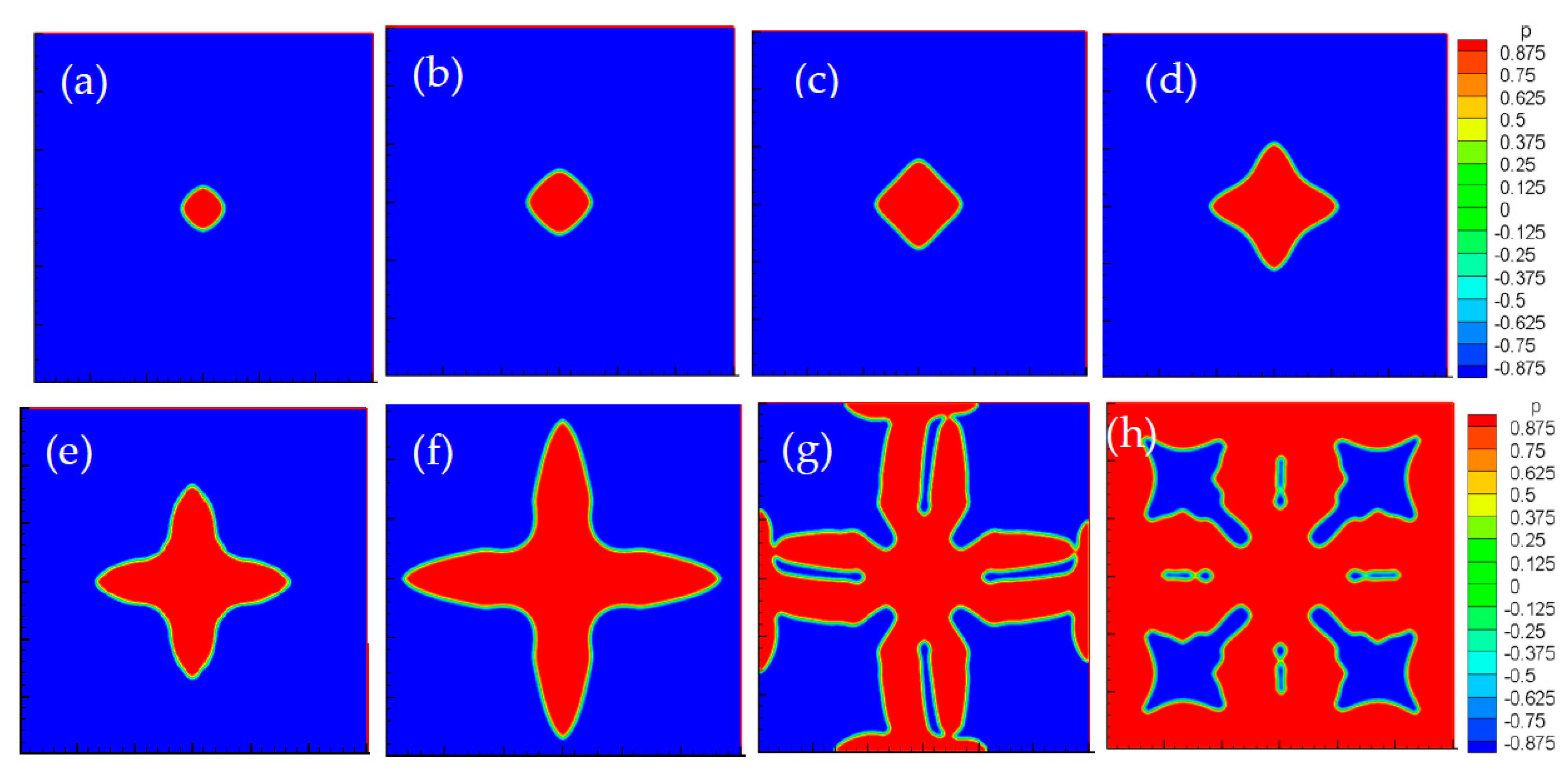
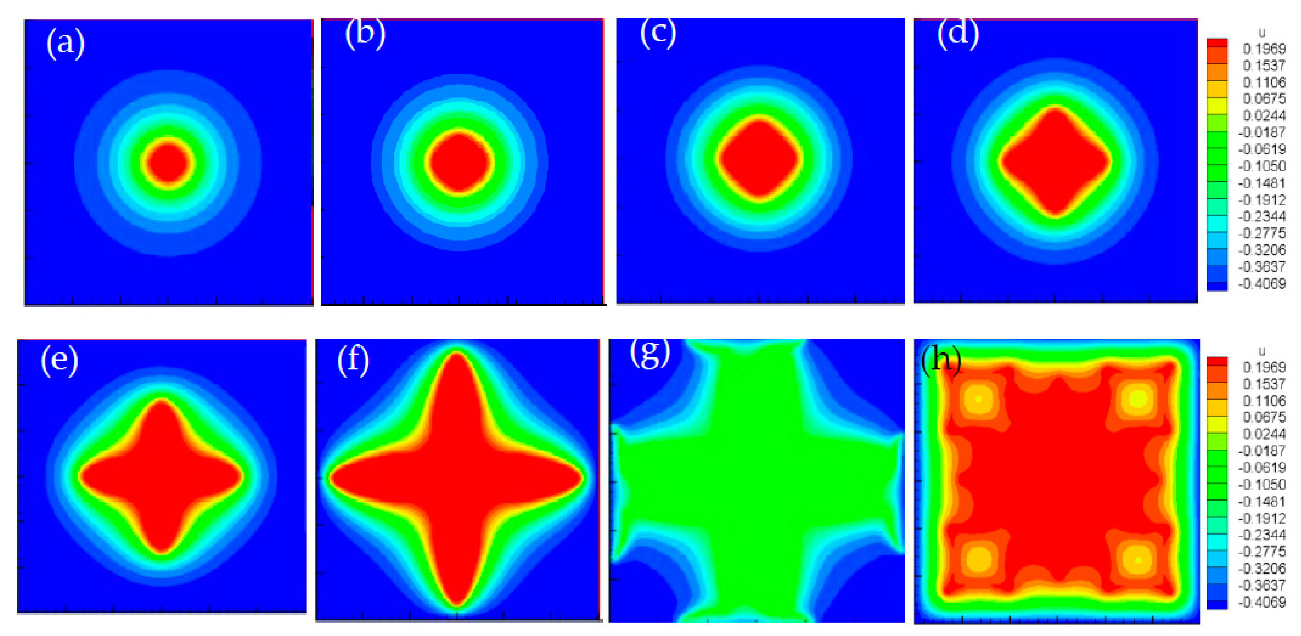
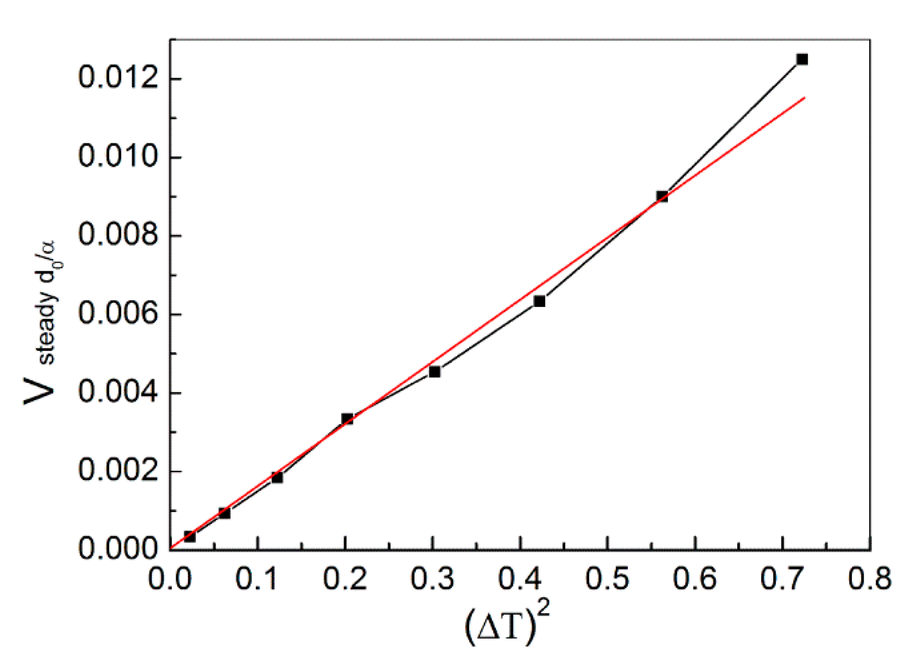
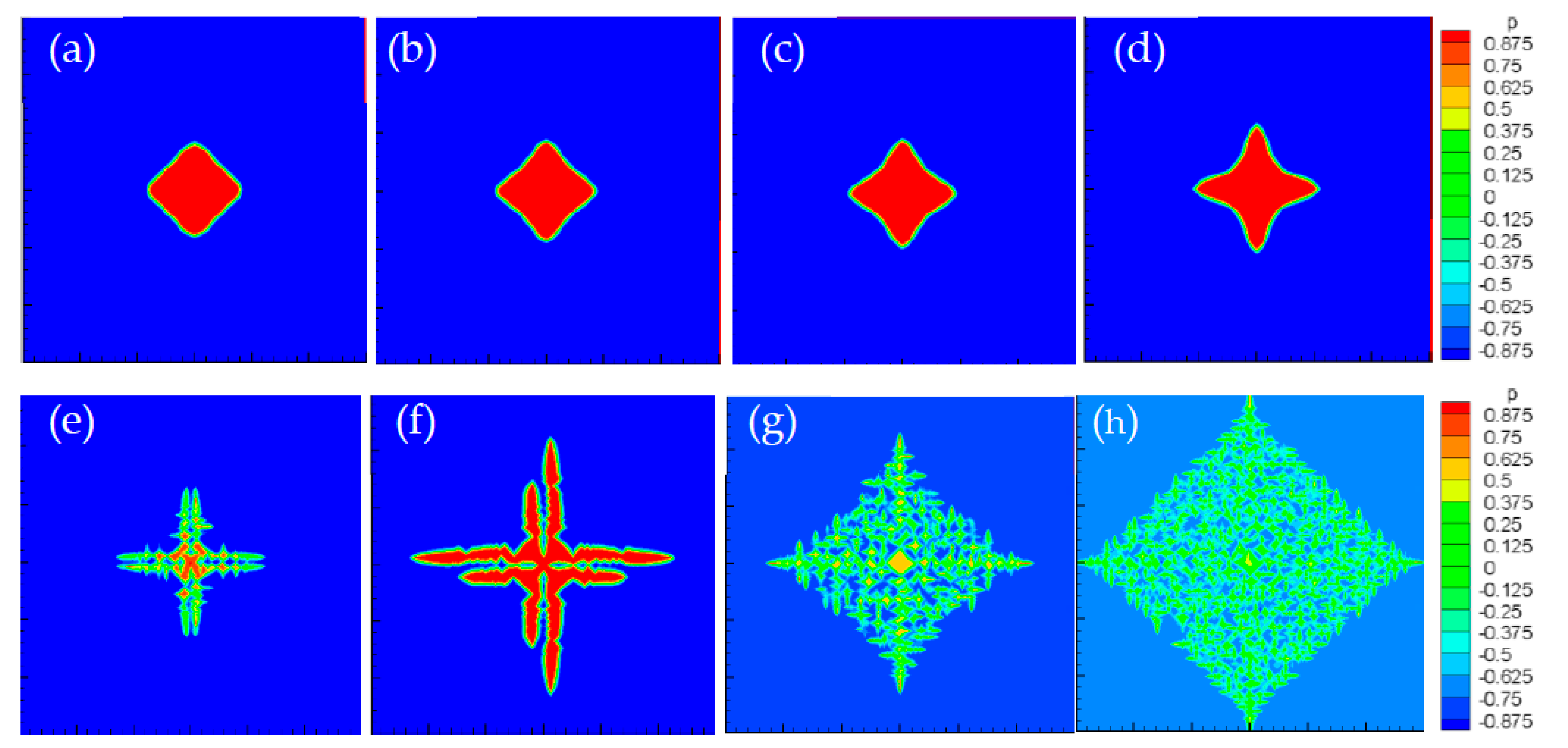
4.1. Influence of Undercooling Degree

The number of grids used for the calculation of the phase field and temperature field of the single-crystal grain is 600 × 600 and the initial crystal nucleus is a circular surface with R = 8 at the center of the grid. The phase field equations and the temperature field equations were solved simultaneously using explicit finite differences. The phase field parameters are γ = 0.04, λ = 6.359, and t = 45,000Δt. Figure 1 shows the effect of undercooling on the microstructure evolution of single-crystal silicon.
The boundary conditions were adiabatic and nucleation and growth were carried out in supercooled melts. With increases in undercooling, the shape of crystal growth changed from square to dendritic. There is a more obvious orientation of dendrite growth with a faster growth rate. The bifurcation behavior occurs as the root of the dendrite grows necking. The main branch of the dendrite is no longer smooth, and the dendrite grows on the facet. The curvature utility disappears. This is because after nucleation, the nuclei grow in the supercooled molten liquid in front. A greater degree of undercooling leads to a faster release of the latent heat of crystallization as growth continues along the direction of the negative temperature gradient in the liquid phase. It is consistent with the result of the experiment by T. Aoyama et al. [7]. The phase field evolution under different undercooling degrees is shown in Figure 1.
The isotherm of the temperature field is shown in Figure 2. The isotherm of the supercooling degree Δ = −0.15~−0.35 is circular, and that of the supercooling degree Δ = −0.45~−0.65 gradually becomes square. There is a large temperature gradient at the tip of the dendrite, and there is a temperature difference across the interface, thus, resulting in an increased heat flux transfer and allowing the tip to dissipate more heat. As a result, the growth rate of dendrites at the tip increased, but the growth rate of dendrites in the four eugenic tips remained the same. The distribution of diffusion layers near each tip was also the same, and the dendrites showed a centrosymmetric morphology. When the undercooling degree is greater than Δ = −0.75, the interface instability temperature field is no longer regular. The crystal growth then changes from a non-facet crystal to a facet crystal.
The difference in free energy of liquid phase and solid phase per unit volume is Δ G V , Δ G V = L m Δ T T m where, Lm is the latent heat of melting, Δ T is the degree of undercooling, and T m is the melting point. The endothermic value is positive and the exothermic value is negative, so Δ G V < 0. The greater the supercooling degree, the greater the absolute value of Δ G V , the greater the driving force of solidification, and the faster the crystal growth rate. The simulation results agree well with the classical solidification theory.
According to the theory related to the step growth of the microscopic smooth interface, if the screw dislocation exists on the crystal surface, the growth step can be provided continuously. The theoretical growth rate is predicted to be V = k(ΔT)2, where V is the growth rate, k’ is the growth rate constant, and Δ T is the supercooling degree. It can be seen from Figure 3 that the theoretical growth rate constant is basically consistent with the simulated growth rate constant. Figure 4 shows the tip grid position of the crystal under different supercooling degrees, which increases with the increase in the supercooling degree.

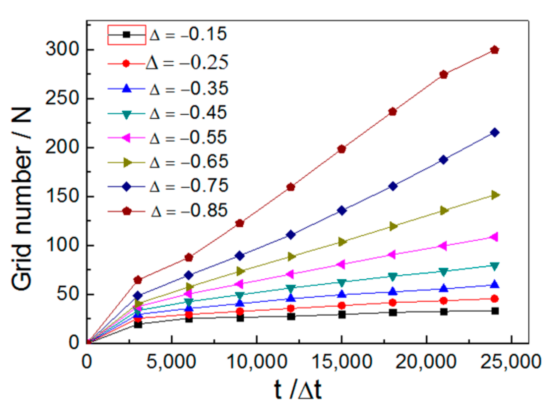
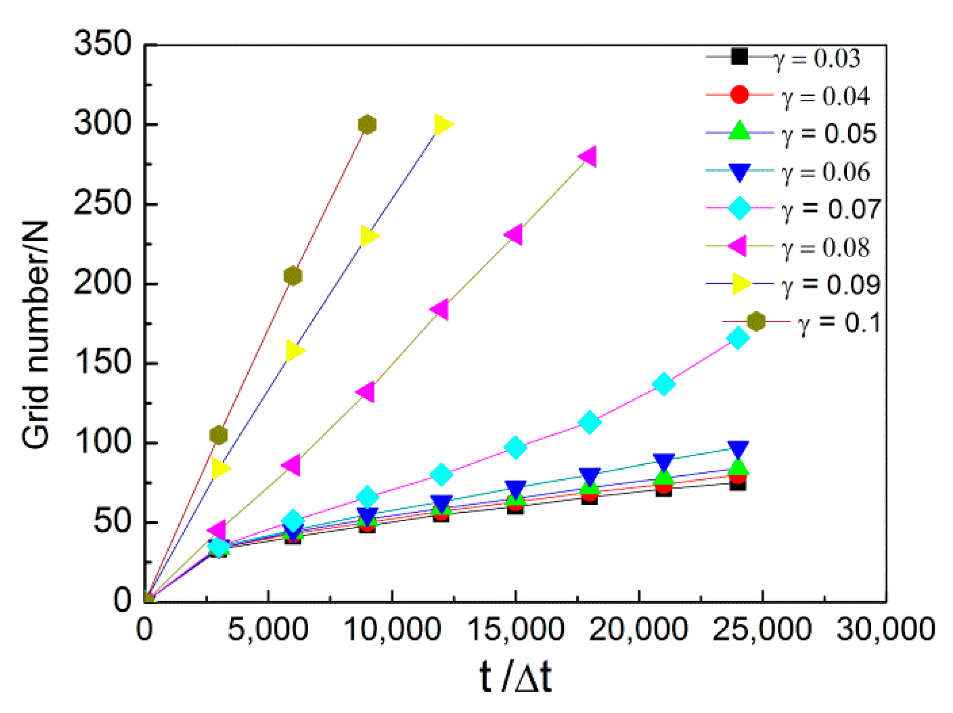
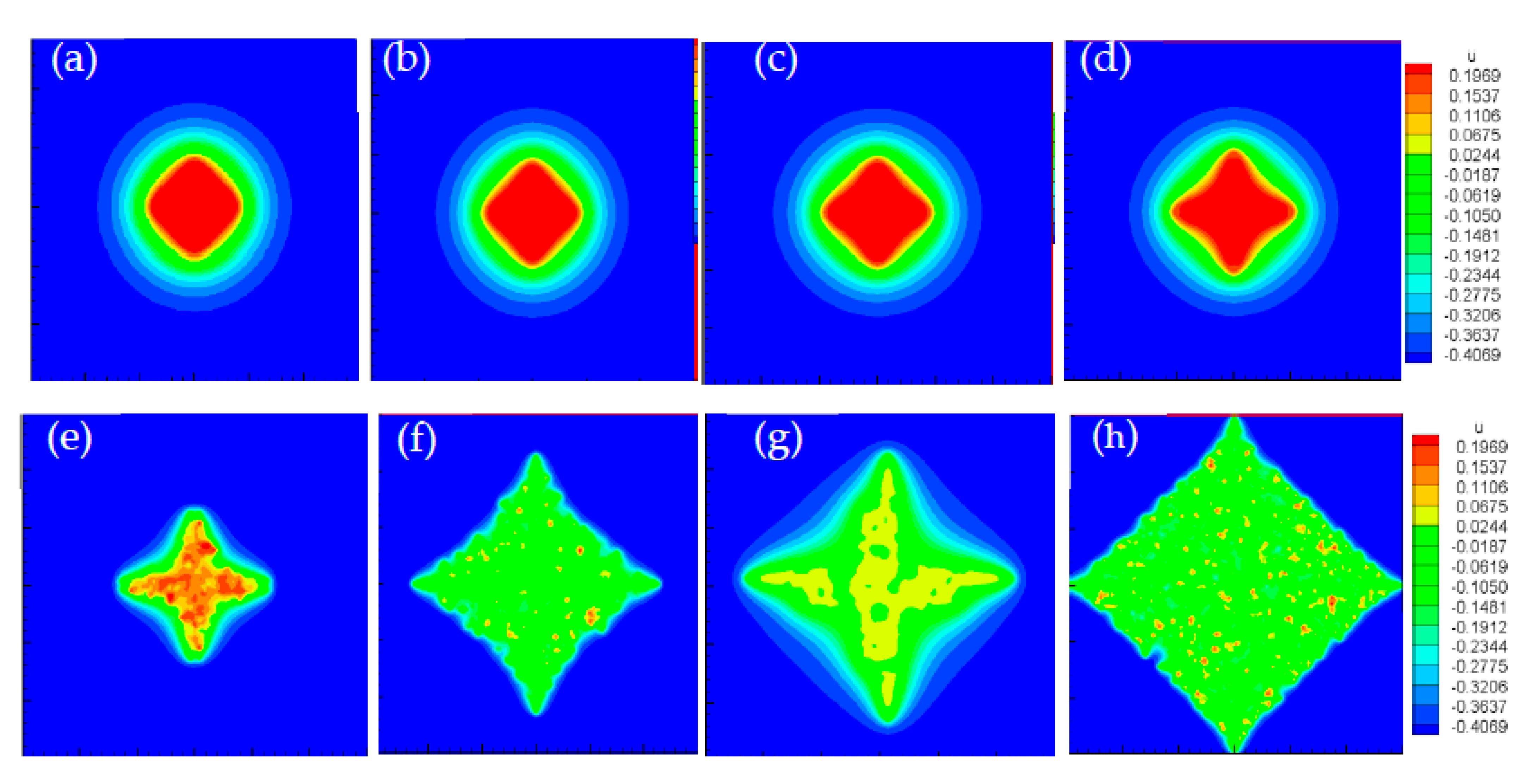
4.2. Influence of the Anisotropy Coefficient

The anisotropy coefficient represents the degree of interfacial surface tension, interfacial thickness, and interfacial dynamic anisotropy. There are many factors affecting anisotropy, and the relationship between the anisotropy coefficient and the material thermophysical parameters remains under study. However, the anisotropy coefficient has a non-negligible effect on the grain growth morphology. The anisotropy of the solid–liquid interface is an important parameter affecting the evolution of crystal growth morphology and the selection of the microstructure.
When Δ = −0.45, λ = 6.359. The grain morphology of the anisotropy coefficient changed sequentially. The growth rate of the crystal tip increases under the conditions of different anisotropy coefficients as the anisotropy coefficient increases (Figure 5). The tip of each crystal is relatively round when the anisotropy coefficient is 0.03~0.05, but the growth rate of the tip is not very different. The main branch end of the dendrite becomes sharper when the anisotropy coefficient is 0.06 and the growth rate increases. Edges and corners appear on the interface when the anisotropy reaches 0.07. The dendrite is no longer smooth, and the morphology changes. The dendrite bifurcates, and the needle-like dendrites parallel to each other appear at the main branch end. The root appears to have an obvious necking phenomenon accompanied by two secondary dendrites. The crystal morphology changes from a non-facet crystal to a facet crystal. The secondary dendrites become more developed when the anisotropy is greater than 0.07. High-order dendrites appear, and the crystal growth rate increases with a more vertical growth direction. The growth rate lowers in the dendrite trunk.
The main branches in each direction are relatively thick when the anisotropy is small. The main branches in each direction become gradually thinner as the anisotropy increases. Excessively large anisotropy will cause dendrite variation because the disturbance is easily amplified when the anisotropy increases. The interface front becomes unstable and the grain morphology changes from non-facet to facet. The phase field is shown in Figure 6.
The corresponding temperature field distribution is shown in Figure 7. The temperature in the solid phase is higher than that in the liquid phase due to the release of latent heat during the growth of dendrites. When the anisotropy coefficient is small, the thickness of the heat diffusion layer in all directions around the solid phase is largely the same, and the temperature growth rate is slow. With increases in the anisotropy coefficient, the heat diffusion layers in the two main axis directions are thinner and the temperature in the main axis direction decreases faster. A larger anisotropy coefficient leads to a thinner diffusion layer around the solid phase. When the anisotropy coefficient is greater than 0.07, no discontinuity can be seen on the temperature field distribution, and the temperature field distribution of the system is not affected.

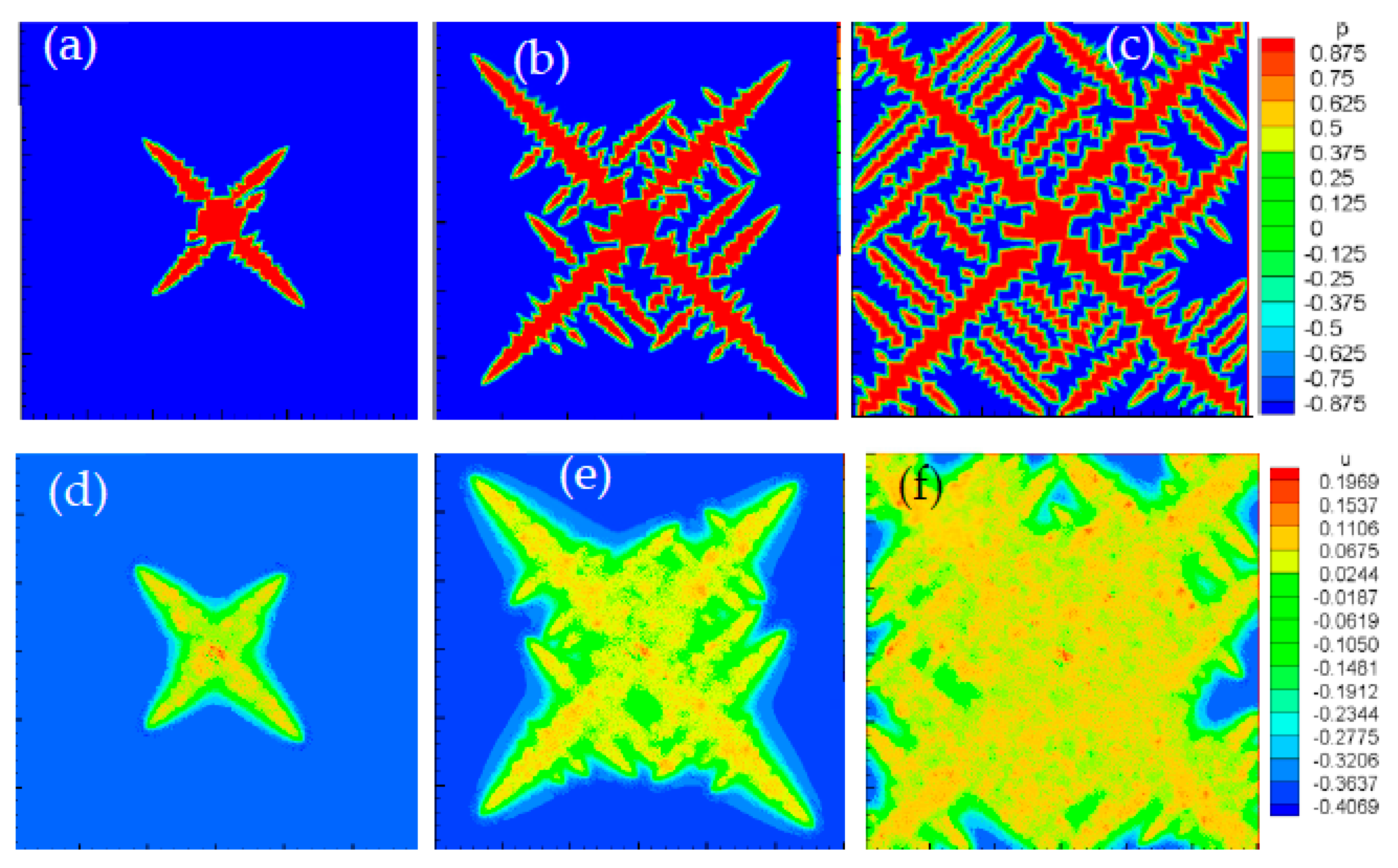
4.3. Selection of the Optimal Direction

The crystal always grows along a preferred direction, and its preferred growth direction is determined by the anisotropy of the crystal. Theoretical analysis, experimental studies, and molecular dynamics calculations show that the anisotropy of growth kinetics plays an important role in the formation of crystal morphology in addition to the anisotropic effect of the interfacial energy.
The infrared image detection of silicon crystals in the production process was carried out as shown in Figure 8. There are different light and dark stripes in the infrared image, indicating that silicon crystals have different growth directions in the growth process. Therefore, the research on preferred direction has certain realistic and theoretical value.
In this paper, the model and dendrite growth algorithm were improved to simulate the crystal morphology growth in any direction. The evolution process of free growth of single-crystal silicon with different preferred growth directions in supercooled melt can be simulated using the improved model and algorithm. Figure 9 shows the crystal growth morphology when the phase field parameters were as follows: γ = 0.15, Δ = −0.55, t = 3000Δt, t = 6000Δt, t = 9000Δt, and the preferred direction is 45°. Secondary dendrites appear on the main branch, and the lengths are different. The center of the dendrites has an obvious necking phenomenon, and the diffusion layers at the tip of the dendrites and the tips of the secondary dendrites are very thin. The heat transfer and dendrite growth are fast.
T. Aoyama et al. [7] conducted experiments on the growth morphology of Si facet dendrites under deep undercooling conditions. The front edge of the interface is an angular discontinuous structure, and many secondary dendrites are generated on the main branch of the dendrite. The root has obvious necking and proliferation effects. Compared to the simulation results of the phase field method, the phase field model established here is qualitatively valid for predicting the growth of small crystal face dendrites.

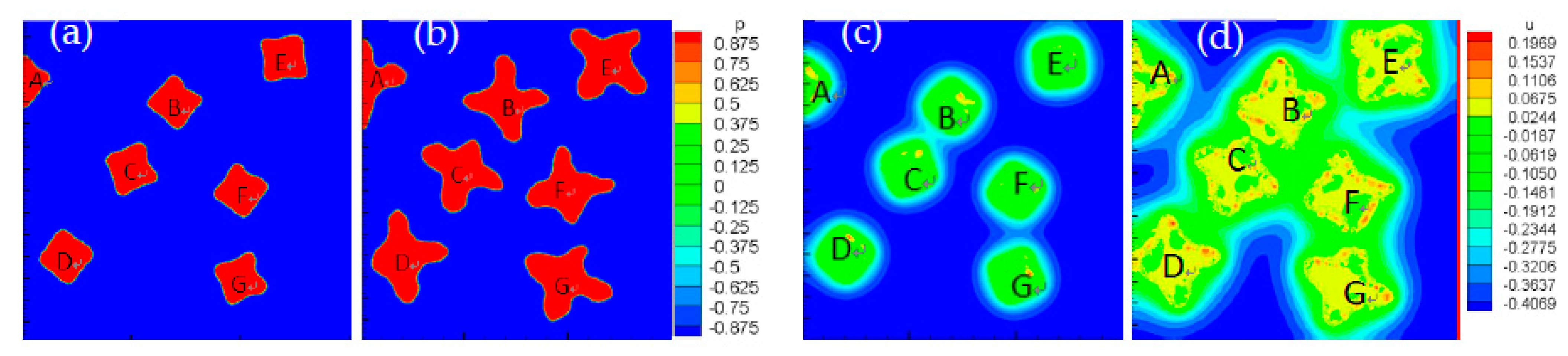
4.4. Multigrain Competitive Growth

The control equation of the phase field was re-optimized based on the phase field model of single dendrite growth of pure material in a single-phase system. An interface free energy anisotropy equation that can simulate the competitive growth of multiple grains was thus established. Using the interface free energy anisotropy function as an independent variable, the interface field governing equation can be derived to control the growth of multiple grains with different optimal orientations, and a phase field model for the competitive growth of single-phase multicrystal grains was established. The number of grids for the multigrain phase field and temperature field calculation was 1500 × 1500, and the number of initial crystal nuclei was seven. The calculation parameters were as follows: γ = 0.04, Δ = −0.45, t = 30,000Δt, and t = 75,000Δt.
Seven nuclei with different preferred directions are randomly placed in the simulation area. In the early stage of solidification, the distance between each dendrite is relatively large, and there is enough space for free growth without mutual influence. Every single grain can grow independently, and their crystal morphology is similar. With the increase in solidification time, the dendrites grow toward each other and affect each other, thus resulting in growth competition. Crystal D is near the boundary of the simulated region (Figure 10). Due to the influence of the simulated boundary conditions, the dendrite branches near the boundary are suppressed and do not completely grow. The temperature fields of other crystals overlap, except for the crystal A grain. The dendrites interact with each other, and the upper main dendrite of grain C is shorter than that of other grains and bends. The lower main dendrite of the C and D grains is bent, and the upper part of dendrite E is due to the boundary conditions bending. This can be explained by growth competition. When there is growth competition between grains, the growth of each grain will release latent heat, and thus, the degree of undercooling there is lower. The grains then move to other areas with a higher degree of undercooling.

5. Conclusions

In this study, the phase field method was used to simulate the competitive growth of polysilicon crystal. The simulation results are in good agreement with the experimental results of other researchers.
(1) The degree of undercooling plays a decisive role in the growth of silicon crystal dendrites. The grain morphology is square when γ = 0.04, Δ = −0.15~−0.35. When Δ = −0.45~−0.65, the grain morphology is smooth and branched. The crystal morphology transforms from non-faceted crystals to faceted crystals when the degree of supercooling exceeds Δ = −0.75.
(2) When the anisotropy is small, the main branches in each direction are relatively thick, and when the anisotropy increases the main branches in each direction gradually become thinner. Edges and corners appear on the interface when the anisotropy increases to 0.07, and the dendrite surfaces are no longer smooth. The material changes from non-faceted to faceted crystals.
(3) The growth morphology of polycrystalline grains in different preferred directions was simulated. When the grains grow toward each other, the initial grains do not affect each other. As the grains grow, they will affect each other. The main branches will inhibit each other so that the length of one main branch of a grain is smaller than that of the other main branches. The growth of the main branch is curved. Compared to existing experimental results, these data more realistically simulate the evolution of polycrystalline silicon crystals.

Author Contributions

Conceptualization, D.Z. and X.Y.; methodology, H.W.; software, D.Z.; validation, X.Y., D.Z. and Q.S.; formal analysis, D.Z.; investigation, X.Y.; resources, X.Y.; data curation, X.Y.; writing—original draft preparation, D.Z.; writing—review and editing, D.Z.; visualization, D.Z.; supervision, D.Z.; project administration, H.W.; funding acquisition, D.Z. All authors have read and agreed to the published version of the manuscript.

Funding

This research was funded by Youth Growth Project of Guizhou Provincial Department of Education, grant number KY (2020) 134.

Institutional Review Board Statement

Not applicable.

Informed Consent Statement

Not applicable.

Data Availability Statement

Not applicable.

Acknowledgments

The author would like to thank the Youth Growth Project of Guizhou Provincial Department of Education, grant number KY (2020) 134, Guizhou Finance Education Fund for Postgraduate Education Reform and Quality Improvement in 2021 (No. 2021055) and the Key Laboratory of Materials Simulation and Computing of Anshun University (Asxyxkpt201803).

Conflicts of Interest

The authors declare no conflict of interest.

References

  1. Wang, W.J.; Wang, S.C. Status and prospect of distributed photovoltaic power generation in my country. J. Chin. Acad. Sci. 2016, 31, 165–172. [Google Scholar]
  2. Su, L.; Hao, Q.Y.; Xie, J.X. Research progress of quasi-single crystal silicon technology. Bull. Silic. 2012, 31, 603–609. [Google Scholar]
  3. Shi, B.C.; Li, K.; Kang, R.G. Technology status and development of casting polysilicon prepared by directional solidification method. Mater. Rev. 2014, 28, 183–187. [Google Scholar]
  4. Fujiwara, K.; Obinata, Y.; Ujihara, T. In-situ Observations of Melt Growth Behavior of Polycrystalline Silicon. J. Cryst. Growth 2004, 262, 124–129. [Google Scholar] [CrossRef]
  5. Fujiwara, K.; Pan, W.; Sawada, K. Directional Growth Method to Obtain High Quality Polycrystalline Silicon from Its Melt. J. Cryst. Growth 2006, 292, 282–285. [Google Scholar] [CrossRef]
  6. Nagashio, K.; Kuribayashi, K. Growth Mechanism of Twin- related and Twin- free Facet Si Dendrites. Acta Mater. 2005, 53, 3021–3029. [Google Scholar] [CrossRef]
  7. Aoyama, T.; Kuribayshi, K. Influence of undercooling on solid/liquidinterface morphology in semiconductors. Acta Mater. 2000, 48, 3739–3744. [Google Scholar] [CrossRef]
  8. Chen, P.; Tsai, Y.L.; Lan, C.W. Phase field modeling of growth competition of silicon grains. Acta Mater. 2008, 56, 4114–4122. [Google Scholar] [CrossRef]
  9. Boettinger, W.J.; Coriell, S.R.; Greer, A.L.; Karma, A.; Kurz, W.; Rappaz, M.; Trivedi, R. Solidification microstructures: Recent developments, future directions. Acta Mater. 2000, 48, 43–70. [Google Scholar] [CrossRef]
  10. Ode, M.; Kim, S.G.; Suzuki, T. Recent Advances in the Phase-Field Model for Solidification. ISIJ Int. 2001, 41, 1076–1082. [Google Scholar] [CrossRef]
  11. Granasy, L.; Borzsonyi, T.; Pusztai, T. Crystal nucleation and growth in binary phase-field theory. Phys. Rev. Lett. 2002, 237, 1813–1817. [Google Scholar]
  12. Granasy, L.; Borzsonyi, T.; Pusztai, T. Phase Field Theory of Heterogeneous Crystal Nucleation. Phys. Rev. Lett. 2007, 98, 035703. [Google Scholar] [CrossRef] [PubMed]
  13. Wendler, F.; Mennerich, C.; Nestler, B. A phase-field model for polycrystalline thin film growth. J. Cryst. Growth 2011, 327, 189–201. [Google Scholar] [CrossRef]
  14. Torabi, S.; Lowengrub, J.; Voigt, A.; Wise, S. A new phase-field model for strongly anisotropic systems. Proc. R. Soc. A Math. Phys. Eng. Sci. 2009, 465, 1337–1359. [Google Scholar] [CrossRef]
  15. Lin, H.K.; Lan, C.W. Three-Dimensional phase field modeling of silicon thin-film growth during directional solidification: Facet formation and grain competition. J. Cryst. Growth 2014, 401, 740–747. [Google Scholar] [CrossRef]
  16. Kasajima, H.; Nagano, E.; Suzuki, T. Phase-Field modeling for facet dendrite growth of silicon. Sci. Technol. Adv. Mater. 2003, 4, 553–557. [Google Scholar] [CrossRef]
  17. Suzuki, T.; Kim, S.G.; Kim, W.T. Two-Dimensional facet crystal growth of silicon from undercooled melt of Si-Ni alloy. Mater. Sci. Eng. A 2007, 449, 99–104. [Google Scholar] [CrossRef]
  18. Chen, Z.; Chen, C.L.; Hao, L.M. Numerical simulation of facet dendrite growth. Trans. Nonferrous Met. Soc. China 2008, 18, 938–943. [Google Scholar] [CrossRef]
  19. Liu, B.Y.; Zhou, Y. Research on interface morphology evolution process of silicon materials using phase field method. Foundry Technol. 2016, 37, 2326–2330. [Google Scholar]
  20. Yuan, X.F.; Yang, Y.; Liu, F. Interface morphology evolution process of solidification for multicrystalline silicon using phase-field method. Sci. Technol. Eng. 2019, 19, 123–128. [Google Scholar]
  21. Zhao, D.P.; Jing, T.; Liu, B.C. Research progress of quasi-single crystal silicon technology. Acta Phys. 2003, 52, 1737–1742. [Google Scholar]
Figure 1. Δt = 45,000. The undercooling is (a) Δ = −0.15; (b) Δ = −0.25; (c) Δ = −0.35; (d) Δ = −0.45; (e) Δ = −0.55; (f) Δ = −0.65; (g) Δ = −0.75; (h) Δ = −0.85. Crystal phase field morphology.
Crystals 12 01271 g001
Figure 2. Δt = 45,000. The undercooling is (a) Δ = −0.15; (b) Δ = −0.25; (c) Δ = −0.35; (d) Δ = −0.45; (e) Δ = −0.55; (f) Δ = −0.65; (g) Δ = −0.75; (h) Δ = −0.85. Crystal temperature field topography.
Crystals 12 01271 g002
Figure 3. The relationship between crystal growth rate and the square of supercooling degree.
Crystals 12 01271 g003
Figure 4. The tip grid positions of crystals at different degrees of supercooling.
Crystals 12 01271 g004
Figure 5. The tip grid positions of crystals with different anisotropy coefficients.
Crystals 12 01271 g005
Figure 6. Δ = −0.45, t = 30,000Δt, (a) γ = 0.03; (b) γ = 0.04; (c) γ = 0.05; (d) γ = 0.06; Δ = −0.45, t = 9000Δt, (e) γ = 0.07; (f) γ = 0.08; (g) γ = 0.09; (h) γ = 0.1. Crystal phase field morphology.
Crystals 12 01271 g006
Figure 7. Δ = −0.45, t = 30000Δt, (a) γ = 0.03; (b) γ = 0.04; (c) γ = 0.05; (d) γ = 0.06; Δ = −0.45, t = 9000Δt, (e) γ = 0.07; (f) γ = 0.08; (g) γ = 0.09; (h) γ = 0.1. Crystal temperature field topography.
Crystals 12 01271 g007
Figure 8. Infrared image of silicon crystal.
Crystals 12 01271 g008
Figure 9. γ = 0.15, Δ = −0.55, (a,b,c) are the phase fields of the silicon crystal at t = 3000Δt, t = 6000Δt, and t = 9000Δt, respectively; (d,e,f) are the temperature fields of the silicon crystal at t = 3000Δt, t = 6000Δt, and t = 9000Δt, respectively.
Crystals 12 01271 g009
Figure 10. γ = 0.04, Δ = −0.45, (a,b) phase fields of polycrystalline silicon crystal at t = 30,000Δt and t = 75,000Δt, respectively; panels (c,d) are the temperature fields of polycrystalline silicon crystal at t = 30,000Δt and t = 75,000Δt, respectively.
Crystals 12 01271 g010
Table 1. Physical properties of silicon.
PropertyValue
Density ρ2570 kg/m3
Melting point Tm1687 K
Thermal conductivity λ66.5 W/k·m
Kinematic viscosity μ8 × 10⁻⁴ Pa·s
Latent heat L1.587 × 106 J/kg
Publisher’s Note: MDPI stays neutral with regard to jurisdictional claims in published maps and institutional affiliations.

