Abstract
NiO thin films deposed on a glass substrate, “NiO/glass”, are successfully prepared using a spray pyrolysis technique (SPT) at 460 °C and characterized via X-ray diffraction (XRD), scanning electron microscopy (SEM), energy dispersive X-ray, Atomic force microscopy (AFM), spectroscopic ellipsometry (SE), Photoluminescence (PL) and diverse electric and magnetic studies. The structural investigation shows that the synthesized films crystallized in a cubic structure with (111) preferential orientation. The NiO layers exhibit a uniform grain of regular sizes with aggregates randomly distributed across their surface. The optical properties of the NiO thin films evidenced a normal optical dispersion as well as good transparency of the NiO films. An unpredicted ferromagnetic aspect was raised due to the high oxygen presence in the synthetized material. A high thermal dependency of the conductivity, as well as a semiconductor behavior of the grown NiO material, is also demonstrated.
1. Introduction
Metal oxides (MOx) semiconductors as inexpensive materials owned fascinating physical properties and excellent chemical stability [1,2,3]. Such characteristics increase their demand in solar cells [4,5], gas sensors [6,7,8], optical windows [9], and acousto-optic devices applications [10,11,12]. They usually exist in n-type transparent conductive oxide (TCO) film. Nevertheless, few of them exist in p-type semiconductors despite their challenging performance [13,14,15,16]. In fact, p-type TCOs are known for their wideband energy bandgap (Eg) varying between 3.6–4.0 eV [17,18,19,20]. NiO is one of the p-type MOx materials crystallized in cubic structure ensuring a good anti-ferromagnetic property [21,22,23,24,25,26] and eminent optical properties [27,28]. Nevertheless, it has not been widely investigated in the industry compared to other MOx semiconductors, such as ZnO and CuO.
In the last decade, NiO thin film synthesis attracted research interest due to its large application in transparent conductive films [29], electrochromic devices [30], organic light-emitting diodes and anodes [30], and chemical sensors as functional layer material [31]. NiO films have been widely synthesized through various physical and chemical routes including plasma-enhanced chemical vapor deposition [32,33,34,35], reactive spraying [36,37,38], pulsed laser deposition [39,40], sol-gel [41], and SPT [42,43,44]. The latest remains one of the most chemical facile routes utilized to prepare NiO films. It is largely applied to prepare films of different components [45]. SPT allows the deposition of films of various thicknesses, multi-layered films, and porous films across a wide surface area [46,47]. NiO sprayed film synthesis starts from a fine droplet token from a solution comprising the chosen substance that is sprayed on the substrate surface after being preheated. This technique guarantees a good crystallization of the films without resorting to any heat treatment cycles using a low-cost raw material and excellent adhesion. Various defects and vacancies accompanied the synthesized films that play a major role in exhibiting new properties [48]. For instance, nickel vacancy affects the conduction and its type. On other hand, the magnetic properties of MOx are influenced by the growth defects [49,50,51].
Several NiO films of uniform thickness have been fabricated via SPT [52]. However, the optimization of the right growth conditions of the NiO films remains a challenge for this technique, where the proper flow rate, substrate temperature, and droplet size vary from one case to another in order to achieve the desired target [53]. Previous works have examined particular growth conditions on the prepared NiO thin films. For instance, Sajilal, et al. [54] succeed in preparing NiO thin layers at different thicknesses using nickel acetate as a precursor at T = 15 K. Nandhini J., et al. [55] also synthesized NiO via an aerosol technique through nickel nitrate, where they reveal its crystallization into a monoclinic structure. Since the properties depend on the structure, S. Viswestwaran, et al. [56] Studied nickel oxide using the electronic paramagnetic resonance technique and deduced the Lande factor. Recently, K.O. Ukoba, et al. [57] similarly reviewed generally the change in the growth conditions′ effect on the fabricated NiO films. Despite the existing work, the optimal synthesizing parameter is still required where no precise flow rate, substrate temperature, and droplet size could be precisely admitted for growing NiO films. Indeed, each synthesized film via SPT requires particular growth conditions to reach the desired research and technology goal. To the best of our knowledge, the optical study of NiO spray thin film from ellipsometry does not investigate so far.
In this context, we report on the current research work on NiO layer synthesis via the spray pyrolysis technique. We represent a broad study of structural, morphological, optical, electric, and magnetic properties of a selected NiO thin film. Our approach differs from those used in earlier works. We have determined the optimal growth conditions such as the concentration of the solution, the constant flow rate, and the deposition time (i.e., thickness), to grow films with high crystallinity. We reported, for the first time, the optical study of NiO spray thin film from ellipsometry. The NiO lattice dependency on the effect of the intrinsic defects has been investigated. Various elements raise defects in the NiO films like chlorine and oxygen. Indeed, we find that the nickel chloride used during the synthesis process leads generally to a high density of defects due to chlorine. This is in addition to the located stress and dislocations derived from the oxygen constructing the NiO material. These defects emerged as an important unpredicted ferromagnetic aspect. We also demonstrate a high thermal dependency of the conductivity as well as a semiconductor behavior of the grown NiO material. We establish a normal optical dispersion and excellent transparency of the NiO films. Such results constitute great finds since they have been archived via a low-cost technique.
2. Experimental Details
2.1. Samples Preparation
Nickel chloride hexahydrate (NiCl2,6H2O) purchased from Sigma Aldrich with purity ≥ 99% was dissolved in deionized water. A 0.01 M of the obtained mixture was agitated with a magnetic stirrer at room temperature until the complete disappearance of the nickel chloride salt. Meantime, chloride acid has been added to ensure a good dissolving of nickel hydroxide formed during NiCl2 dissolution. The substrate, i.e., glass was cleaned ultrasonically via ethanol, Acetic acid, and deionized water and then naturally dried in air. We used a constant flow rate of 4 mL/min through a 0.5 mm diameter nozzle during the spray process at 460 °C. Nitrogen has been used as a carrier gas at a pressure equal to 0.35 bar. We fixed the plane distance in-between the nozzle-substrate to 27 cm [58]. Then, the samples were cooled naturally in the air. We may resume the growth process as below:
- − The formation mechanism of nickel oxide:

- − The residual nickel hydroxide obtained via spray process at 460 °C through an acid-base reaction:

- − Nickel hydroxide transformed into oxide NiO:

2.2. Samples Characterization
X-ray diffractometer (Analytical X Pert PROMPD) with monochromatized copper-source (λ = 1.54056 Å) scanned the samples from 20 to 90°. The morphological properties have been investigated initially using an SEM. We operate with a JEOL-JSM 5400 model SEM supplied by an EDX spectroscopy for elemental microanalysis. Further morphological investigations have been carried out via AFM through VEECO digital instrument 3A apparatus in tapping mode. The optical properties have been characterized with a GES5 SOPRA ellipsometer equipped with a rotating polarizer in the wavelength range between 250–900 nm (4.97–1.38 eV) for an incidence angle of 75° and a xenon arc lamp light source. The existing optical fiber cut the light beam from the light source output to the polarizer input. Then, the polarizer converts random polarization of the light state into a linearly polarized light that illuminates and reflects on the sample surface. The polarized state of the reflected light is determined by combining the rotating analyzer and the photonic detector. The optical calculations have been accomplished with Winelli_II software. A VSM has been addressed to investigate the magnetic properties. Such an instrument ensures rapid measurements and neutralization from parasitic drifts, where it exemplified signals eliminated by synchronous detection by measuring the induced flow in a winding by periodic displacement of the sample. This clarifies VSM characterization where the displacement of the sample at the center of a measuring coil with a constant amplitude vibrates vertically (z-axis) at a fixed frequency of 200 Hz. The electric conductivity of NiO films has been examined via a four-point probe in the temperature range [150–450 °C].
3. Results and Discussions
3.1. Structural Characterizations
3.1.1. Structural Parameters Determination
XRD measurements showed a typical pattern of NiO sprayed thin films (see, Figure 1). We located the well-defined NiO peaks (111), (002), (022), and (222). These latest orientations correspond to the cubic structure NiO according to the JCPDS card 040-835 [59,60]. Indeed, the NiO film grown here is highly oriented following the (111) direction. Therefore, the NiO films grown here have a cubic structure along with the (111) orientation [59,60].
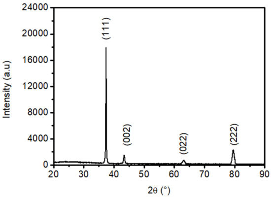
Figure 1.
XRD diffractogram of the synthesized NiO films.
The interplanar spacing “dhkl” and lattice parameter “a” were determined using the correlation between the Bragg formula and the characteristic relation of the cubic phase [35,61,62]. We reported in Table 1 the calculated values of interplanar spacing and lattice parameters.

Table 1.
Interplanar distance “dhkl” and lattice parameter “a” of NiO sprayed thin films.
3.1.2. Defect Impact on the Change of the Lattice Parameter
The lattice parameter “a” shows a slight difference compared to that known for NiO powder [61]. This could be assigned to the local defect in the prepared NiO films. This confirms the changes in the X-ray diffraction peaks width obtained here. Indeed, the structural defects could be seen in terms of crystallite size as micro-strain and dislocation density. These are determined via the following relation [62,63,64]:
where k = 0.90 is the Scherrer constant and β1/2 the corrected half-width of the peak.
Table 2 represents the values of the crystallite size, micro-strain, and dislocation density values for the different orientations. The obtained results prove the origin of the lattice parameter “a” change in the NiO film, which is associated with the local defect. Indeed, the crystallite size is larger than the mesh size in all orientations. Thus, the crystallites are formed from a large number of meshes which make some properties of the synthesized thin NiO film close to the ideal case.
Table 2.
Values of crystallite size D, dislocation density ε, micro-strain δ and texture coefficient TC of NiO films.
3.1.3. Crystallite Formation Proof
The probability of crystallite growth could be determined by the mean values of the structural parameters related to the texture coefficient (TC) obtained by XRD measurements. The texture coefficient (TC) of the maximum preferred orientation (hkl) plane “TC (h k l)” is deducted from the XRD spectrum according to the following formula [63,64]:
where I (hkl) represents the measured relative intensity of (hkl) plane, I0(hkl) is the standard intensity of the same plane taken from the JCPDS 040-835, and N indicates the reflection number.
The TC (hkl) values of the NiO sprayed films confirm that the orientation of the crystallites is along (111) direction [63,64]. Admitting that TC (h kl) may give an indication about the probability of crystallite formation. The mean values of the structural parameters, i.e., the crystallites size <D>, the residual stress <ε>, and the dislocation density <δ> could be found using Williamson and Hall relations [65,66]:
Table 3 resumes the average calculated values of crystallite size, dislocation density, and micro-strain of NiO films. It is possible then to estimate the number of meshes per crystallites as reported in [67,68] using the following relation:
Table 3.
NiO films average values of crystallite size, dislocation density, and micro-strain.
The probability of crystallite growth is assigned to the number of meshes per crystallite. Herein, we estimated the number of meshes per crystallite in NiO prepared films, we found it equal to ≈8.709 × 10⁶. The obtained finite number is coherent with the presence of the defects. Indeed, as mentioned by E. Blanc, et al. [69], the typical dimension of the crystallite in the ideal case assigned to a single crystal must be higher than 1 µm. Thus, for nickel oxide, such a dimension corresponds to at least 1012 meshes per crystallite. This latest is greater than the estimated value in our NiO films. This confirms the defect influence on the growing NiO films where it reduces the meshes per crystallites.
3.2. Morphological Investigation
The growth mechanism, the quality, and the topography of the NiO films have been studied by correlating both SEM and AFM. The SEM images of NiO films across a large area of the sample (≈100 μm) illustrate a rough surface with pores randomly located (see, Figure 2a). At high magnifications, this image clearly confirms a typical microstructure of the NiO thin film (see, Figure 2b). The observed roughness comes from a nonhomogeneous visible grain with a regular shape through the NiO film (see, Figure 2b). The located grains showed a large size variety, where their sizes change from 200 nm to 400 nm (see, Figure 2b). Similarly, wide pores have been found to induce a porous aspect to the NiO film (see, Figure 2b). Other aggregates, i.e., surface defects have been also located. Such defects are mainly formed during a deposition process. Their origin could be attributed to the residual wet phases and some hydrochloric acid molecules penetrating pores.
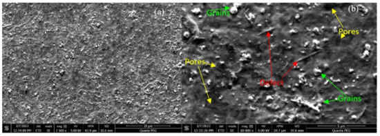
Figure 2.
SEM image of the NiO film surfaces: (a) across 100 μm of the sample surface, (b) on a small area of the sample covering 20 μm.
We also studied a 3 × 3 μm2 area across the sample surface using AFM microscopy to image the morphology of the synthesized NiO film. Figure 3a illustrates the 2D AFM images of the NiO sprayed films. A rough surface of the NiO film has been located similarly to that seen with SEM. Herein, a high-intensity region with grains like that revealed by SEM appeared clearly, with a good precision of their size and shape (see, Figure 3a). Additionally, weak intensity regions have been located where minor roughness could be reported assigned to the pores observed in SEM. Therefore, AFM measurements are consisting of SEM results. For better imaging, we represented this area using a 3D image (see, Figure 3b). This latest confirms the presence of grains and pores.
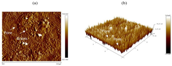
Figure 3.
AFM images of the synthesized NiO films: (a) 2D, (b) 3D image.
3.3. EDX Analysis
For a better analysis of the binary material ratio in the NiO prepared films. Nickel and oxygen stoichiometric ratios have been determined using EDX analysis (see, Figure 4). We located three main Ni peaks at around 1 keV, 7.5 keV, and 8.4 keV, respectively. Another peak has been observed at 0.5 keV which corresponds to oxygen. On the other hand, a fifth peak was also found near 2.8 keV. This latest could be originated from residual chloride descending from the protocol followed for the growth process. We also deduced the weight and atomic percentage of nickel and oxygen in the grown NiO thin films from EDX measurements. Table 4 summarizes the related mass and atomic percentages of the elements oxygen and nickel. We found an atomic ratio of [O]/[Ni] slightly higher than 1 (≈1.040) highlighting the p-type of the NiO material synthesized here.
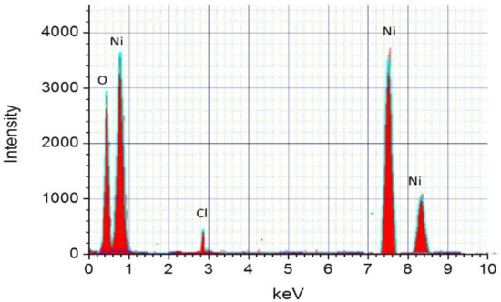
Figure 4.
EDX spectrum of NiO sprayed thin films.
Table 4.
Chemical compositions in NiO films.
The root means square roughness (Rms) usually expressed as the average square deviation from the mean line within the assessment length L (see, Figure 4). Indeed, Rms is given by the relation [70,71,72]:
We found Rm in the order of 20 nm. It is less than of the sample thickness which demonstrates promising optical applications of the grown NiO films.
3.4. Dispersion Parameters
We studied the optical properties of NiO films with SE. A simplified diagram of the ellipsometry measuring device is given in Figure 5. This technique is a self-referencing technique, measuring the polarization states before and after reflection. It is based on the interaction of polarized light with a sample described by the Jones matrix formalism [73,74,75]:
where Eip and Eis correspond to the parallel (p) and perpendicular (s) components of the incident electric field beam light(i), while Ers and Ers are assigned to the reflected (r) ones. and correspond to the complex Fresnel reflection coefficients of the sample for both polarization p and s, correspondingly. The coefficients and are equal to zero since the cubic structure is isotropic.
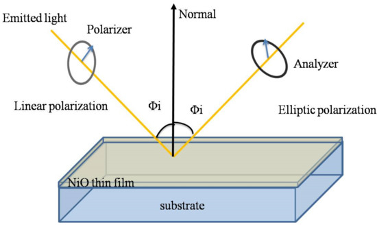
Figure 5.
General geometry light path in an ellipsometer.
The and coefficient expressed for the simple ambient/material case in the top panel of Figure 5 are given by the following relations [75]:
where δp and δs correspond to the phase changes for the parallel (p) and perpendicular (s) components upon reflection.
Since NiO crystallizes in a cubic structure. This imposes an isotropic optical property on the material. In this case, the off-diagonal terms Rps and Rsp describe the cross-coupling of both p- and s-polarized light and become zero. On the other hand, ellipsometry normally describes both parameters: the amplitude ratio upon reflection tanΨ(λ) and the phase shift difference between p and s polarizations Δ(λ). These parameters determine several optical properties, i.e., the refractive index n(λ) and the extinction coefficient k(λ). They are described by using the following equation [76]:
where and Δ(λ) corresponds to Δ = δp − δs.
The experimental and simulated study of tan(Ψ) and cos(Δ) with their standard deviation and average values have been addressed to verify the obtained optical results (see, Figure 6a,b). The ratio (ρ) is related to the complex dielectric function, ε = ε1 + iε2, by the following relation [77,78]:
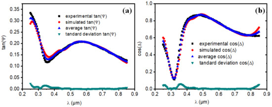
Figure 6.
(a) Experimental, simulated, average experimental, and standard deviation plot of tan(Ψ), (b) Experimental, simulated, average experimental, and standard deviation plot of cos(Δ).
Both results, i.e., experimental and simulated, of tan(Ψ) and cos(Δ) demonstrate a good coherence. The standard deviation has been found also partially zero. This confirms our findings and gives the reliability to the calculated optical parameters via ellipsometry measurements and Winelli_II software.
We could determine the dispersion parameter, i.e., the refractive index n(λ) and the extinction coefficient k(λ) using the obtained dielectric parameter. This is using the three following relations [76,79]:
ε(λ) = (n(λ) + ik(λ))2 = ε1(λ) + iε2(λ)
ε1(λ) = n2 − k2
ε2(λ) = 2n*k
Figure 7 images the n(λ) and k(λ) change. We located a decrease in the value of the extinction coefficient k, where it reaches a low value in the visible range. This illustrates the high transparency of binary materials. However, we found that the extinction coefficient k increased with the wavelength in the infrared domain. This is assigned mainly to the free carrier, mainly the holes. This demonstrates that nickel deficiencies in NiO films induce a p-type character in the semiconductor.
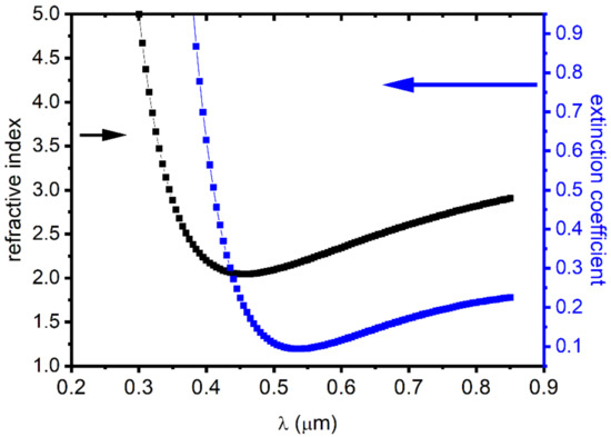
Figure 7.
The extinction coefficient and refractive index variations as a function of the wavelength.
3.5. Magnetic Properties
NiO materials display particular magnetic properties [80,81,82]. The saturation magnetization (Ms), the remanent magnetization (Mr), and the coercivity (Hc) of the NiO thin films have been studied using M-H hysteresis loops at room temperature (see, Figure 8). The associated values have been given in Table 5 after subtracting the magnetic contribution of the glass substrate from the overall magnetic behavior. The NiO films display a typical ferromagnetic behavior, despite the anti-ferromagnetic nature of the NiO material [83,84,85]. This unique magnetic effect found here could be related to the: non-stoichiometric defect. Indeed, the prepared thin films contain some defects such as stress and dislocations. This explains the structural defect and Weiss domains in the grown NiO thin films. Here, a minor interaction between domains may cause results that limit the polarization of the material with the coming magnetic field. This induces a ferromagnetic behavior of these films. On the other hand, nickel oxide as binary material is a p-type semiconductor [86]. This p-type has a non-stoichiometric defect that emerged due to the dual effect of chlorine and the excess oxygen. Indeed, the nickel chloride used during the synthesis process leads to a high density of defects due to chlorine that become pronounced when added to the local defect originated by oxygen forming NiO material. This stoichiometric defect may result in such a ferromagnetic behavior. Our find is consistent with previous studies. Indeed, a close ferromagnetic behavior has been reported for NiO powder at high and room temperature [87,88]. This confirms our results obtained for NiO thin film.
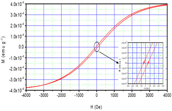
Figure 8.
M–H loops of NiO sprayed thin film.
Table 5.
Values of Coercivity (Hc), Magnetization (Ms), and Retentivity (Mr) of NiO thin films.
3.6. Electrical Properties
The electrical conductivity of the NiO films has been investigated via four points probe at different temperatures. The measurements at each temperature were performed after reaching the thermodynamic equilibrium (i.e., the stabilization of the temperature). The four probes have been arranged linearly, i.e., in a straight line equally distanced from each other. Herein, the potential drop V is measured across the middle of the two probes after the passage of a constant current through them. Meanwhile, the high-temperature effect on the sample has been considered after exposing it to an oven. Figure 9 illustrates the variation of Ln(σT) as a function of (1000/T). This image the electrical conductivity variation with temperature. The thermal conductivity exhibited a semiconductor behavior. Indeed, we found a linear decrease of Ln(σT) versus 1000/T, which confirms that the electrical conductivity follows the Arrhenius law [89,90,91]:
where A is a constant and is the activation energy.
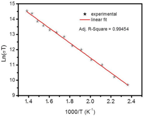
Figure 9.
Temperature dependence of DC conductivity σDC.
The calculated activation energy value is equal to 0.5 eV. The obtained energy is smaller than that of . This proves that NiO cannot be considered an intrinsic semiconductor under our current measurement conditions.
4. Conclusions
In the present work, we reported NiO layers synthesis via the spray pyrolysis technique. A diverse structural, morphological, optical, electric, and magnetic properties of NiO thin film have been revealed. We represent a new approach by specifying the optimal: concentration of the solution, the constant flow rate, and the deposition time. A quasi-monocrystalline structure has been demonstrated for the prepared NiO film with a preferential (111) direction. For the first time, the optical study of NiO spray thin film from ellipsometry has been given here. We illustrated NiO lattice dependency to the effect of the intrinsic defect. Various elements induce defects in the NiO films like chlorine and oxygen. Indeed, nickel chloride used in the synthesis process generates a high density of defects due to chlorine. This is in addition to the located stress and dislocations derived from the oxygen constructing the NiO material. Such defects arose an important unpredicted ferromagnetic aspect. A high thermal dependency of the conductivity, as well as a semiconductor behavior of the grown NiO material, have been revealed. We establish a normal optical dispersion and excellent transparency of the NiO films. Our findings archived herein via a low-cost technique will facilitate the synthesis of NiO films and open the door for their application in industry. A further study is in progress to reach electro-optical properties and magneto-electrical properties in terms of the colossal magneto-resistance properties.
Author Contributions
Conceptualization A.B.G.T., A.B., H.E. investigation, A.B.G.T., F.H.A., A.Z., A.B., M.G., H.E.; formal analysis A.B.G.T., F.H.A., A.Z., A.B., M.G.; methodology, A.B.G.T., F.H.A., A.Z., A.B., M.G.; Data curation, A.B.G.T., F.H.A., A.Z., A.B., M.G.; writing—original draft preparation, A.B.G.T., F.H.A., A.B.; writing—review and editing, A.B.G.T., F.H.A., A.Z., A.B., M.G., H.E.; supervision H.E.; All authors have read and agreed to the published version of the manuscript.
Funding
This research was funded by Princess Nourah bint Abdulrahman University Researchers Supporting Project number (PNURSP2022R223), Princess Nourah bint Abdulrahman University, Riyadh, Saudi Arabia.
Institutional Review Board Statement
Not applicable.
Informed Consent Statement
Not applicable.
Data Availability Statement
Not applicable.
Acknowledgments
The authors express their gratitude to Princess Nourah bint Abdulrahman University Researchers Supporting Project number (PNURSP2022R223), Princess Nourah bint Abdulrahman University, Riyadh, Saudi Arabia.
Conflicts of Interest
The authors declare no conflict of interest.
References
- Ros, C.; Andreu, T.; David, J.; Arbiol, J.; Morante, J.R. Degradation and regeneration mechanisms of NiO protective layers deposited by ALD on photoanodes. Mater. Chem. A 2019, 7, 21892–21902. [Google Scholar] [CrossRef]
- Othmen, W.B.H.; Hamed, Z.B.; Sieber, B.; Addad, A.; Elhouichet, H.; Boukherroub, R. Structural and optical characterization of p-type highly Fe-doped SnO2 thin films and tunneling transport on SnO2: Fe/p-Si heterojunction. Appl Surf Sci. 2018, 434, 879–890. [Google Scholar] [CrossRef]
- Taeño, M.; Maestre, D.; Cremades, A. An approach to emerging optical and optoelectronic applications based on NiO micro and nanostructures. Nanophotonics 2021, 10, 1785–1799. [Google Scholar] [CrossRef]
- Sharma, R.; Acharya, A.D.; Shrivastava, S.B.; Shripathi, T.; Ganesan, V. Preparation and characterization of transparent NiO thin films deposited by spray pyrolysis technique. Optik 2014, 125, 6751–6756. [Google Scholar] [CrossRef]
- Kim, K.H.; Takahashi, C.; Abe, Y.; Kawamura, M. Effects of Cu doping on nickel oxide thin film prepared by sol–gel solution process. Optik 2014, 125, 2899–2901. [Google Scholar] [CrossRef]
- Girolamo, D.D.; Giacomo, F.D.; Matteocci, F.; Marrani, A.G.; Dini, D.; Abate, A. Progress, highlights and perspectives on NiO in perovskite. Photovoltaics 2020, 11, 7746–7759. [Google Scholar]
- Michalska, M.; Surmiak, M.A.; Maasoumi, F.; Senevirathna, D.C.; Chantler, P.; Li, H.; Li, B.; Zhang, T.; Lin, X.; Deng, H.; et al. Microfluidic Processing of Ligand-Engineered NiO Nanoparticles for Low-Temperature Hole-Transporting Layers in Perovskite Solar Cells. Sol. RRL 2021, 5, 2100342. [Google Scholar] [CrossRef]
- Wilson, R.L.; Simion, C.E.; Stanoiu, A.; Taylor, A.; Guldin, S.; Covington, J.A.; Carmalt, C.J.; Blackman, C.S. Humidity-Tolerant Ultrathin NiO Gas-Sensing Films. ACS Sens. 2020, 5, 1389–1397. [Google Scholar] [CrossRef]
- Mokoena, T.P.; Swart, H.C.; Motaung, D.E. A review on recent progress of p-type nickel oxide based gas sensors: Future perspectives. J. Alloys Compd. 2019, 805, 267–294. [Google Scholar] [CrossRef]
- Luan, C.; Wang, K.; Yu, Q.; Lian, G.; Zhang, L.; Wang, Q.; Cui, D. Improving the gas-sensing performance of SnO2 porous nanosolid sensors by surface modification. Sens. Actuators B 2013, 176, 475. [Google Scholar] [CrossRef]
- Kobayashi, T.; Kumazawa, T.; Kaoa, Z.J.L.; Nakada, T. Cu(In, Ga)Se2 thin film solar cells with a combined ALD-Zn(O, S) buffer and MOCVD-ZnO:B window layers. Sol. Energy Mater. Sol. Cells 2013, 119, 129. [Google Scholar] [CrossRef]
- Shih, W.C.; Wang, M.J.; Lin, I.N. Characteristics of ZnO thin film surface acoustic wave devices fabricated using nanocrystalline diamond film on silicon substrates. Diam. Relat. Mater. 2008, 17, 390. [Google Scholar] [CrossRef]
- Fu, Y.Q.; Luo, J.K.; Du, X.Y.; Flewitt, A.J.; Li, Y.; Markx, G.H.; Walton, A.J.; Milne, W.I. Recent developments on ZnO films for acoustic wave-based bio-sensing and microfluidic applications: A review. Sens. Actuators B 2010, 143, 606. [Google Scholar] [CrossRef]
- Krishnamoorthy, S.; Iliadis, A.A. Properties of high sensitivity ZnO surface acoustic wave sensors on SiO2/(100) Si substrates. Solid-State Electron. 2008, 11, 1710–1716. [Google Scholar] [CrossRef]
- Bonomo, M.; Dini, D.; Decker, F. Electrochemical and Photoelectrochemical Properties of Nickel Oxide (NiO) With Nanostructured Morphology for Photoconversion Applications. Front. Chem. 2018, 6, 601. [Google Scholar] [CrossRef] [PubMed]
- Diao, C.C.; Huang, C.Y.; Yang, C.F.; Wu, C.C. Morphological, Optical, and Electrical Properties of p-Type Nickel Oxide Thin Films by Nonvacuum Deposition. Nanomaterials 2020, 10, 636. [Google Scholar] [CrossRef] [Green Version]
- Li, M.-H.; Yum, J.-H.; Moon, S.-J.; Chen, P. Inorganic p-Type Semiconductors: Their Applications and Progress in Dye-Sensitized Solar Cells and Perovskite Solar Cells. Energies 2016, 9, 331. [Google Scholar] [CrossRef] [Green Version]
- Manojreddy, P.; Itapu, S.; Ravali, J.K.; Sakkarai, S. Tuning the Electrical Parameters of p-NiOx-Based Thin Film Transistors (TFTs) by Pulsed Laser Irradiation. Condens. Matter 2021, 6, 21. [Google Scholar] [CrossRef]
- Reguig, B.A.; Khelil, A.; Cattin, L.; Morsli, M.; Bernède, J.C. Properties of NiO thin films deposited by intermittent spray pyrolysis process. Appl. Surf. Sci. 2007, 253, 4330–4334. [Google Scholar] [CrossRef]
- Hosny, N.M. Synthesis, characterization and optical band gap of NiO nanoparticles derived from anthranilic acid precursors via a thermal decomposition route. Polyhedron 2011, 30, 470–476. [Google Scholar] [CrossRef]
- Meybodi, S.M.; Hosseini, S.A.; Rezaee, M.; Sadrnezhaad, S.K.; Mohammadyani, D. Synthesis of wide band gap nanocrystalline NiO powder via a sonochemical method. Ultrason. Sonochem. 2012, 19, 841–845. [Google Scholar] [CrossRef] [PubMed]
- Nakajima, N.; Kato, H.; Sakisak, Y. Surface metallic nature caused by an in-gap state of reduced NiO: A photoemission study. J. Electron Spectrosc. Relat. Phenom. 2005, 144–147, 873–875. [Google Scholar] [CrossRef]
- Eder, R. Electronic structure of NiO: Antiferromagnetic transition and photoelectron spectra in the ordered phase. Phys. Rev. B 2015, 91, 245146. [Google Scholar] [CrossRef] [Green Version]
- Thota, S.; Shim, J.H.; Seehra, M.S. Size-dependent shifts of the Néel temperature and optical band-gap in NiO nanoparticles. J. Appl. Phys. 2013, 114, 214307. [Google Scholar] [CrossRef]
- Guo, S.; Liu, W.; Liu, X.H.; Gong, W.J.; Feng, J.N.; Zhang, Z.D. Influence of ferromagnetic layer on the exchange coupling of antiferromagnetic NiO-based films. J. Magn. Magn. Mater. 2012, 324, 3933. [Google Scholar] [CrossRef]
- Nkosi, S.S.; Yalisi, B.; Motaung, D.E.; Keartland, J.; Sideras-Haddadb, E.; Forbes, A.; Mwakikung, B.W. Antiferromagnetic–paramagnetic state transition of NiO synthesized by pulsed laser deposition. Appl. Surf. Sci. 2013, 265, 860. [Google Scholar] [CrossRef]
- Mokoena, T.P.; Swart, H.C.; Hillie, K.T.; Tshabalala, Z.P.; Jozela, M.; Tshilongo, J.; Motaung, D.E. Enhanced propanol gas sensing performance of p-type NiO gas sensor induced by exceptionally large surface area and crystallinity. Appl. Surf. Sci. 2022, 571, 151121. [Google Scholar] [CrossRef]
- Kaya, D.; Aydınoğlu, H.S.; Tüzemen, E.S.; Ekicibil, A. Investigation of optical, electronic, and magnetic properties of p-type NiO thin film on different substrates. Thin Solid Films 2021, 732, 138800. [Google Scholar] [CrossRef]
- Pereira, S.; Gonçalves, A.; Correia, N.; Pinto, J.; Pereira, L.; Martins, R.; Fortunato, E. Electrochromic behavior of NiO thin films deposited by e-beam evaporation at room temperature. Sol. Energy Mater Sol. Cells 2014, 120, 109. [Google Scholar] [CrossRef]
- Moulki, H.; Faure, C.; Mihelčič, M.; ŠurcaVuk, A.; Švegl, F.; Orel, B.; Campet, G.; Alfredsson, M.; Chadwick, A.V.; Gianolio, D.; et al. Electrochromic performances of nonstoichiometric NiO thin films. Thin Solid Films 2014, 553, 63. [Google Scholar] [CrossRef]
- Chen, S.C.; Kuo, T.Y.; Lin, Y.C.; Chang, C.L. Preparation and properties of p-type transparent conductive Cu-doped NiO films. Adv. Mater. Res. 2010, 123, 181. [Google Scholar] [CrossRef]
- Korosec, R.C.; Bukovec, P. Sol–gel prepared NiO thin films for electrochromic applications. Acta Chim. Slov. 2006, 53, 136. [Google Scholar]
- Gowthami, V.; Perumal, P.; Sivakumar, R.; Sanjeeviraja, C. Structural and optical studies on nickel oxide thin film prepared by nebulizer spray technique. Phys. B 2014, 452, 1. [Google Scholar] [CrossRef]
- Boukhachem, A.; Boughalmi, R.; Karyaoui, M.; Mhamdi, A.; Chtourou, R.; Boubaker, K.; Amlouk, M. Study of substrate temperature effects on structural, optical, mechanical and opto-thermal properties of NiO sprayed semiconductor thin films. Mater. Sci. Eng. B 2014, 188, 72. [Google Scholar] [CrossRef]
- Puspharajah, P.; Radhakrishna, S.; Arof, A.K. Transparent conducting lithium-doped nickel oxide thin films by spray pyrolysis technique. J. Matcr. Sci. 1997, 32, 3001. [Google Scholar] [CrossRef]
- Nigro, R.L.; Battiato, S.; Greco, G.; Fiorenza, P.; Roccaforte, F.; Malandrino, G. Metal Organic Chemical Vapor Deposition of nickel oxide thin films for wide band gap device technology. Thin Solid Films 2014, 563, 50. [Google Scholar] [CrossRef]
- Mat-Teridi, M.A.; Tahir, A.A.; Senthilarasu, S.; Wijayantha, K.G.U.; Sulaiman, M.Y.; Ahmad-Ludin, N.; Ibrahim, M.A.; Sopian, K. Fabrication of NiO photoelectrodes by aerosol-assisted chemical vapour deposition (AACVD). Phys. Status Solidi-Rapid Res. Lett. 2014, 8, 982. [Google Scholar] [CrossRef]
- Yeh, W.C.; Matsumura, M. Chemical vapor deposition of nickel oxide films from bis-π-cyclopentadienyl-nickel. Jpn. J. Appl. Phys. 1997, 36, 6884. [Google Scholar] [CrossRef]
- Reddy, Y.A.K.; Reddy, A.S.; Reddy, P.S. Effect of oxygen partial pressure on the properties of NiO–Ag composite films grown by DC reactive magnetron sputterin. J. Alloys Compd. 2014, 583, 396. [Google Scholar] [CrossRef]
- Chen, S.C.; Wen, C.K.; Kuo, T.Y.; Peng, W.C.; Lin, H.C. Characterization and properties of NiO films produced by rf magnetron sputtering with oxygen ion source assistance. Thin Solid Films 2014, 572, 51. [Google Scholar] [CrossRef]
- Wang, Y.; Zhang, F.; Wei, L.; Li, G.; Zhang, W. Facet-dependent photocatalytic performance of NiO oriented thin films prepared by pulsed laser deposition. Phys. B 2014, 457, 194. [Google Scholar] [CrossRef]
- Chan, I.M.; Hong, F.C. Improved performance of the single-layer and double-layer organic light emitting diodes by nickel oxide coated indium tin oxide anode. Thin Solid Films 2004, 450, 304. [Google Scholar] [CrossRef]
- Hotovy, I.; Huran, J.; Siciliano, P.; Capone, S.; Spiess, L.; Rehacek, V. Enhancement of H 2 sensing properties of NiO-based thin films with a Pt surface modification. Sens Actuator B Chem. 2004, 103, 300. [Google Scholar] [CrossRef]
- Patil, P.S.; Kadam, L.D. Preparation and characterization of spray pyrolyzed nickel oxide (NiO) thin films. Appl. Surf. Sci. 2002, 199, 211–221. [Google Scholar] [CrossRef]
- Udayakumar, R.; Khanaa, V.; Saravanan, T. Synthesis and structural characterization of thin films of SnO 2 prepared by spray pyrolysis technique. Indian J. Sci. Technol. 2013, 6, 4754–4757. [Google Scholar] [CrossRef]
- Ilegbusi, O.J.; Khatami, S.N.; Trakhtenberg, L.I. Spray Pyrolysis deposition of single and mixed oxide thin films. Mater. Sci. Appl. 2017, 8, 153. [Google Scholar] [CrossRef] [Green Version]
- Messing, G.L.; Zhang, S.C.; Jayanthi, G.V. Ceramic powder synthesis by spray pyrolysis. J. Am. Ceram. Soc. 1993, 76, 2707–2726. [Google Scholar] [CrossRef]
- Verma, V.; Katiyar, M. Effect of the deposition parameters on the structural and magnetic properties of pulsed laser ablated NiO thin films. Thin Solid Films 2013, 527, 369. [Google Scholar] [CrossRef]
- Turgut, G.; Sonmez, E.; Duman, S. Determination of certain sol-gel growth parameters of nickel oxide film. Ceram. Int. 2015, 41, 2976. [Google Scholar] [CrossRef]
- Egbo, K.O.; Liu, C.P.; Ekuma, C.E.; Yu, K.M. Vacancy defects induced changes in the electronic and optical properties of NiO studied by spectroscopic ellipsometry and first-principles calculations. J. Appl. Phys. 2020, 128, 135705. [Google Scholar] [CrossRef]
- Mokoena, T.P.; Swart, H.C.; Hillie, K.T.; Motaung, D.E. Engineering of rare-earth Eu3+ ions doping on p-type NiO for selective detection of toluene gas sensing and luminescence properties. Sens. Actuators B Chem. 2021, 347, 130530. [Google Scholar] [CrossRef]
- Nehru, L.; Umadevi, M.; Sanjeeviraja, C. Studies on structural, optical and electrical properties of ZnO thin films prepared by the spray pyrolysis method. Int. J. Mater. Eng. 2012, 2, 12–17. [Google Scholar] [CrossRef] [Green Version]
- Patil, P.S. Versatility of chemical spray pyrolysis technique. Mater. Chem. Phys. 1999, 59, 185–198. [Google Scholar] [CrossRef]
- Sajilal, K.; Raj, A.M.E. Effect of thickness on structural and magnetic properties of NiO thin films prepared by chemical spray pyrolysis (CSP) technique. Mater. Lett. 2016, 164, 547–550. [Google Scholar] [CrossRef]
- Usharani, N.J.; Bhattacharya, S.S. Effect of defect states in the optical and magnetic properties of nanocrystalline NiO synthesised in a single step by an aerosol process. Ceram. Inter. 2020, 46, 5671. [Google Scholar] [CrossRef]
- Visweswaran, S.; Venkatachalapathy, R.; Haris, M.; Murugesan, R. Structural, morphological, optical and magnetic properties of sprayed NiO thin flms by perfume atomizer. Appl. Phys. A 2020, 126, 524. [Google Scholar] [CrossRef]
- Ukoba, K.O.; Eloka-Eboka, A.C.; Inambao, F.L. Review of nanostructured NiO thin film deposition using the spray pyrolysis technique. Renew. Sust. Energ. Rev. 2018, 82, 2900–2915. [Google Scholar] [CrossRef]
- Park, J.W.; Choi, K.N.; Baek, S.H.; Chung, K.S.; Hosun, L.E.E. Optical Properties of NiO Thin Films Grown by Using Sputtering Deposition and Studied with Spectroscopic Ellipsometry. J. Korean Phys. Soc. 2008, 52, 1868–1876. [Google Scholar] [CrossRef]
- Lu, H.L.; Scarel, G.; Alia, M.; Fanciulli, M.; Ding, S.J.; Zhang, D.W. Spectroscopic ellipsometry study of thin NiO films grown on Si (100) by atomic layer deposition. Appl. Phys. Lett. 2008, 92, 222907. [Google Scholar] [CrossRef]
- Boubaker, K.; Chaouachi, A.; Amlouk, M.; Bouzouita, H. Enhancement of pyrolysis spray disposal performance using thermal time-response to precursor uniform deposition. Eur. Phys. J. Appl. Phys. 2007, 37, 105. [Google Scholar] [CrossRef]
- Mighell, A.D.; Hubbard, C.R.; Stalick, J.K.; Holomany, M.A. NBS*AIDS83: A Manual Describing the Data Format Used in NBS*AIDS83; JCPDS-International Centre for Diffraction Data: Swarthmore, PA, USA, 1983. [Google Scholar]
- Bergerhoff, G.; Brown, I.D. Crystallographic Databases; International Union of Crystallography: Chester, UK, 1987. [Google Scholar]
- Padhan, A.M.; Alagarsamy, P. Investigation of NiO reduction dynamics and properties of NiO-Ti powders. J. Alloy. Compds. 2020, 840, 155769. [Google Scholar] [CrossRef]
- Amor, M.B.; Boukhachem, A.; Boubaker, K.; Amlouk, M. Structural, optical and electrical studies on Mg-doped NiO thin films for sensitivity applications. Mater. Sci. Semicond. Process. 2014, 27, 994. [Google Scholar] [CrossRef]
- Loukil, A.; Boukhachem, A.; Amor, M.B.; Ghamnia, M.; Raouadi, K. Effects of potassium incorporation on the structural, optical, vibrational and electrical properties of NiO sprayed thin films for p-type optical windows. Ceram. Int. 2016, 42, 8274. [Google Scholar] [CrossRef]
- Chakhoum, M.A.; Boukhachem, A.; Ghamnia, M.; Benameur, N.; Mahdhi, N.; Raouadi, K.; Amlouk, M. An attempt to study (111) oriented NiO-like TCO thin films in terms of structural, optical properties and photocatalytic activities under strontium doping. Spectrochim. Acta Part A Mol. Biomol. Spectrosc. 2018, 205, 649. [Google Scholar] [CrossRef]
- Reddy, A.J.; Kokila, M.K.; Nagabhushana, H.; Sharma, S.C.; Rao, J.L.; Shivakumara, C.; Nagabhushana, B.M.; Chakradhar, R.P.S. Structural, EPR, photo and thermoluminescence properties of ZnO:Fe nanoparticles. Mater. Chem. Phys. 2012, 133, 876. [Google Scholar] [CrossRef]
- Mahdi, M.A.; Hassan, Z.; Ng, S.S.; Hassan, J.J.; MohdBakhori, S.K. Structural and optical properties of nanocrystalline CdS thin films prepared using microwave-assisted chemical bath deposition. Thin Solid Films 2012, 520, 3477. [Google Scholar] [CrossRef]
- Boughalmi, R.; Rahmani, R.; Boukhachem, A.; Amrani, B.; Driss-Khodja, K.; Amlouk, M. Metallic behavior of NiS thin film under the structural, optical, electrical and ab initio investigation frameworks. Mater. Chem. Phys. 2015, 163, 99–106. [Google Scholar] [CrossRef]
- Jaballah, R.; Gassoumi, B.; Othmani, A.; Loukil, A.; Boukhachem, A.; Ghamnia, M.; Kamoun-Turki, N.; Amlouk, M. Synthesis, structural, electrical and electrochemical investigations of CoNi2S4 thin films for solid fuel applications. Opt.—Int. J. Light Electron Opt. 2021, 242, 167003. [Google Scholar] [CrossRef]
- Blanc, E.; Schwarzenbach, D.; Flack, H.D. The evaluation of transmission factors and their first derivatives with respect to crystal shape parameters. J. Appl. Crystallogr. 1991, 24, 1035–1041. [Google Scholar] [CrossRef]
- Ristova, M.; Kuo, Y.; Lee, S. Influence of the roughness of molybdenum back electrode on the photodiode characteristics under He–Ne illumination. Semicond. Sci. Technol. 2003, 18, 788. [Google Scholar] [CrossRef]
- Boukhachem, A.; Bouzidi, C.; Boughalmi, R.; Ouerteni, R.; Kahlaoui, M.; Ouni, B.; Elhouichet, H.; Amlouk, M. Physical investigations on MoO3 sprayed thin film for selective sensitivity applications. Ceram. Int. 2014, 40, 13427. [Google Scholar] [CrossRef]
- Boukhachem, A.; Mokhtari, M.; Benameur, N.; Ziouche, A.; Martínez, M.; Petkova, P.; Ghamnia, M.; Cobo, A.; Zergoug, M.; Amlouk, M. Structural optical magnetic properties of Co doped α-MoO3 sprayed thin films. Sens. Actuators A 2017, 253, 198. [Google Scholar] [CrossRef]
- Azzam, R.M.A.; Bashara, N.M. Ellipsometry and Polarized Light; North-Holland: New York, NY, USA, 1977. [Google Scholar]
- Gonzalez-Fuentes, C.; Gonzalez-Diaz, J.B.; Fallarino, L.; Arregi, J.A.; Berger, A. Influence of the light incidence angle on the precision of generalized magneto-optical ellipsometry. Magn. Magn. Mater. 2015, 386, 150. [Google Scholar] [CrossRef]
- Sampath, U.; Kim, H.; Kim, D.G.; Kim, Y.C.; Song, M. In-situ cure monitoring of wind turbine blades by using fiber Bragg grating sensors and Fresnel reflection measurement. Sensors 2015, 15, 18229. [Google Scholar] [CrossRef] [PubMed] [Green Version]
- Sdiri, N.; Boukhachem, A.; Dhahri, E. Optical investigations of la07ca0.3-xkxmno3 (x = 0.00, 0.05 and 0.10) probed by spectroscopic ellipsometry. Ceram. -Silikáty 2012, 56, 95. [Google Scholar]
- Kumari, N.; Krupanidhi, S.B.; Varma, K.B.R. Structural and electrical characterization of Bi2VO5.5/Bi4Ti3O12 bilayer thin films deposited by pulsed laser ablation technique. Mater. Res. Bull. 2010, 45, 465. [Google Scholar] [CrossRef] [Green Version]
- Aspnes, D.E. Approximate solution of ellipsometric equations for optically biaxial crystals. J. Opt. Soc. Am. 1980, 70, 1275. [Google Scholar] [CrossRef]
- Boukhachem, A.; Ouni, B.; Karyaoui, M.; Madani, A.; Chtourou, R.; Amlouk, M. Structural, opto-thermal and electrical properties of ZnO:Mo sprayed thin films. Mater. Sci. Semicond. Process. 2012, 15, 282. [Google Scholar] [CrossRef]
- Arabi, H.; Moghadam, N.K. Nanostructure and magnetic properties of magnesium ferrite thin films deposited on glass substrate by spray pyrolysis. J. Magn. Magn. Mater. 2013, 335, 144. [Google Scholar] [CrossRef]
- Wang, J.; Sun, J.; Sun, Q.; Chen, Q. Magnetic Iron Oxide Nanoparticles: Synthesis and Surface Functionalization Strategies. Mater. Res. Bull. 2003, 38, 1113. [Google Scholar] [CrossRef]
- Che, S.; Wang, J.; Chen, Q. Soft magnetic nanoparticles of BaFe12O19 fabricated under mild conditions. J. Phys. Condens. Matter 2003, 15, L335. [Google Scholar] [CrossRef]
- Gandhi, A.; Pant, J.; Pandit, S.D.; Dalimbkar, S.K.; Chan, T.S.; Cheng, C.L.; Ma, Y.R.; Wu, S.Y. Short-Range Magnon Excitation in NiO Nanoparticle. J. Phys. Chem. C 2013, 117, 18666–18674. [Google Scholar] [CrossRef]
- Bhide, V.G.; Shenoy, G.K. Fe57 Mössbauer Effect in Nickel Oxide. Phys. Rev. 1966, 143, 309. [Google Scholar] [CrossRef]
- Bartel, L.C.; Morosin, B. Exchange Striction in NiO. Phys. Rev. B 1971, 3, 1039. [Google Scholar] [CrossRef]
- Echresh, A.; Chey, C.O.; Shoushtari, M.Z.; Khranovskyy, V.; Nur, O.; Willander, M. UV photo-detector based on p-NiO thin film/n-ZnO nanorods heterojunction prepared by a simple process. J. Alloys Compd. 2015, 632, 165. [Google Scholar] [CrossRef] [Green Version]
- Kisan, B.; Saravanan, P.; Layek, S.; Verma, H.C.; Hesp, D.; Dhanak, V.; Krishnamurthy, S.; Perumal, A. Effect of annealing on the magnetic properties of ball milled NiO powders. J. Magn. Magn. Mater. 2015, 384, 296. [Google Scholar] [CrossRef]
- Layek, S.; Verma, H.C. Room temperature ferromagnetism in Mn-doped NiO nanoparticles. J. Magn. Magn. Mater. 2016, 397, 73. [Google Scholar] [CrossRef]
- Mott, N.F. Conduction in non-crystalline materials. Philos. Mag. 1969, 19, 835. [Google Scholar] [CrossRef]
Publisher’s Note: MDPI stays neutral with regard to jurisdictional claims in published maps and institutional affiliations. |
© 2022 by the authors. Licensee MDPI, Basel, Switzerland. This article is an open access article distributed under the terms and conditions of the Creative Commons Attribution (CC BY) license (https://creativecommons.org/licenses/by/4.0/).