Article

Transport Properties of the Two-Dimensional Hole Gas for H-Terminated Diamond with an Al2O3 Passivation Layer

1
National Key Laboratory of ASIC, Hebei Semiconductor Research Institute, Shijiazhuang 050051, China
2
School of Electronic and Information Engineering, Xi’an Jiaotong University, Xi’an 710049, China
*
Author to whom correspondence should be addressed.
Crystals 2022, 12(3), 390; https://doi.org/10.3390/cryst12030390
Submission received: 14 February 2022 / Revised: 3 March 2022 / Accepted: 10 March 2022 / Published: 14 March 2022
(This article belongs to the Special Issue 2D Crystalline Nanomaterials)

Abstract

:
Diamonds are thought to be excellent candidates of next-generation semiconductor materials for high power and high frequency devices. A two-dimensional hole gas in a hydrogen-terminated diamond shows promising properties for microwave power devices. However, high sheet resistance and low carrier mobility are still limiting factors for the performance improvement of hydrogen-terminated diamond field effect transistors. In this work, the carrier scattering mechanisms of a two-dimensional hole gas in a hydrogen-terminated diamond are studied. Surface roughness scattering and ionic impurity scattering are found to be the dominant scattering sources. Impurity scattering enhancement was found for the samples after a high-temperature Al2O3 deposition process. This work gives some insight into the carrier transport of hydrogen-terminated diamonds and should be helpful for the development of diamond field effect transistors.

1. Introduction

Due to its high critical breakdown electric field, high carrier saturation drift velocity, high thermal conductivity, and high carrier mobility, diamonds have great application potential in high power and high frequency areas [1]. A hydrogen-terminated (H-terminated) diamond surface demonstrates a relatively high surface conductivity due to the forming of a two-dimensional hole gas (2DHG) by transfer doping from adsorbates/dielectric materials in contact with a H-terminated diamond surface. The electron transfer from the diamond to the adsorbates/dielectric materials and the holes accumulate in the subsurface of the H-terminated diamond [2,3]. The 2DHG shows a sheet density of 1012 to 1013 cm2 and a carrier mobility of less than 200 cm2/(V·s) [4,5,6].
H-terminated diamond field effect transistors (FETs) have obtained good direct current (DC) and radio frequency (RF) performances. A drain current density (IDSmax) of 1.3 A/mm [7] and a maximum oscillation frequency (fmax) of 120 GHz [8] have been obtained for H-diamond FETs. Recently, the output power density was also improved and reached 3.8 W/mm at 1 GHz [9]. Output power densities at 2 GHz [10] and 10 GHz [11] were also reported. However, for high power and high frequency applications, the sheet resistance of the 2DHG is still at a high level and the carrier mobility is low, which leads to large parasitic resistance and limits the performance of H-terminated diamond FETs. Another issue is that, in the fabrication process of H-terminated diamond FETs, a gate dielectric, such as Al2O3 deposition, is needed, which is usually performed at a high temperature. The surface adsorbates would be broken during the high temperature process, which influences the electrical properties of the 2DHG of the H-terminated diamond. The atomic layer deposition (ALD) Al2O3 films are gate insulator and passivation films for the p-type surface conduction of the H-terminated diamond surface. Many works have investigated the effects of Al2O3 passivation films [12,13,14]. Kawarada et al. [12,15] suggested that the surface adsorbates desorbed below 250 °C. There are defects in the ALD Al2O3 films, which introduce unoccupied levels above the valence band edge of Al2O3. The defects could accept the electrons transferring from the H-terminated diamond and be negatively charged. Ren et al. deposited an Al2O3 film at 300 °C and found that O impurity or Al vacancy defects existed in the ALD Al2O3 dielectric. Additionally, the ALD Al2O3 dielectric can work as an acceptor-like transfer doping material on the H-terminated diamond surface [16]. Liu et al. deposited Al2O3 at 120, 200, and 300 °C. They found that, when the deposition temperature of ALD Al2O3 was increased from 120 to 300 °C, the polarity of the fixed charges in the ALD Al2O3 dielectric changes from positive to negative [17]. The low carrier mobility of the 2DHG of the H-terminated diamond has been one of the limiting factors for the development of H-terminated diamond FETs. Some works have investigated the carrier scattering mechanism of the H-terminated diamond [18,19]. The deposition of Al2O3 may introduce an extra scattering source to the 2DHG of the H-terminated diamond and influence its electrical properties. However, to date, no report on the scattering mechanism analysis has been conducted for the Al2O3/H-terminated diamond structure.
In this work, the influence of Al2O3 deposition by a high-temperature ALD process on the transport properties of the 2DHG in a H-terminated diamond is investigated. The sheet resistance, carrier density, and mobility of H-diamond samples with and without Al2O3 were measured from 90 to 300 K by a Van der Pauw–Hall method. The temperature dependence of the mobility of the 2DHG is fitted considering four scattering mechanisms: ionic impurity (IM) scattering, acoustic phonon (AC) scattering, optical phonon (OP) scattering, and surface roughness (SR) scattering for the H-diamond samples with and without Al2O3 deposition.

2. Experiments

Three kinds of H-terminated diamond samples were prepared, as shown in Figure 1. The samples were prepared by the microwave plasma CVD (MPCVD, Seki diamond systems, Japan) technique. For the SC-Epitaxial H-termination samples, the samples were a single crystal diamond with a H-termination formed by a homoepitaxial growth process as stated in [20]. The microwave power was 1 kW, and growth temperature was 900 °C with a chamber pressure of 100 Torr. The CH4/H2 ratio was 1% with total flow of 500 sccm. For the SC-H plasma treatment and PC-H plasma treatment samples, the samples were treated by MPCVD in H2 plasma [21]. The hydrogen plasma treatment was performed at a chamber pressure of 5 kPa and a temperature of 800 °C for 40 min. The SC-H plasma treatment samples were a single crystal diamond, and the PC-H plasma treatment samples were a polycrystalline diamond with a grain size of ~100 μm. The electrical properties of the H-terminated diamond samples were measured by the Van der Pauw–Hall method in the low temperature Hall measurement system from 90 K to 300 K.

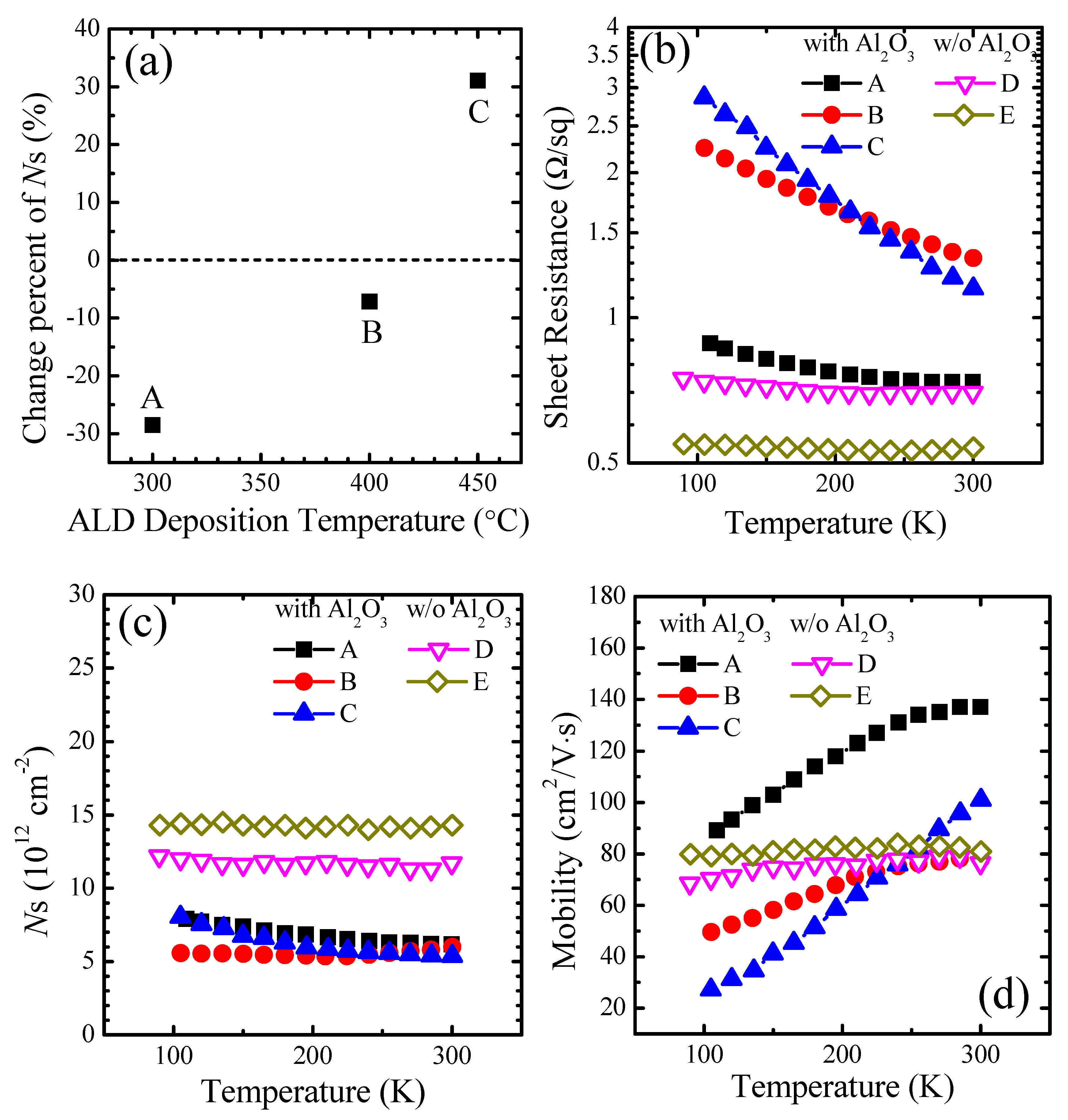
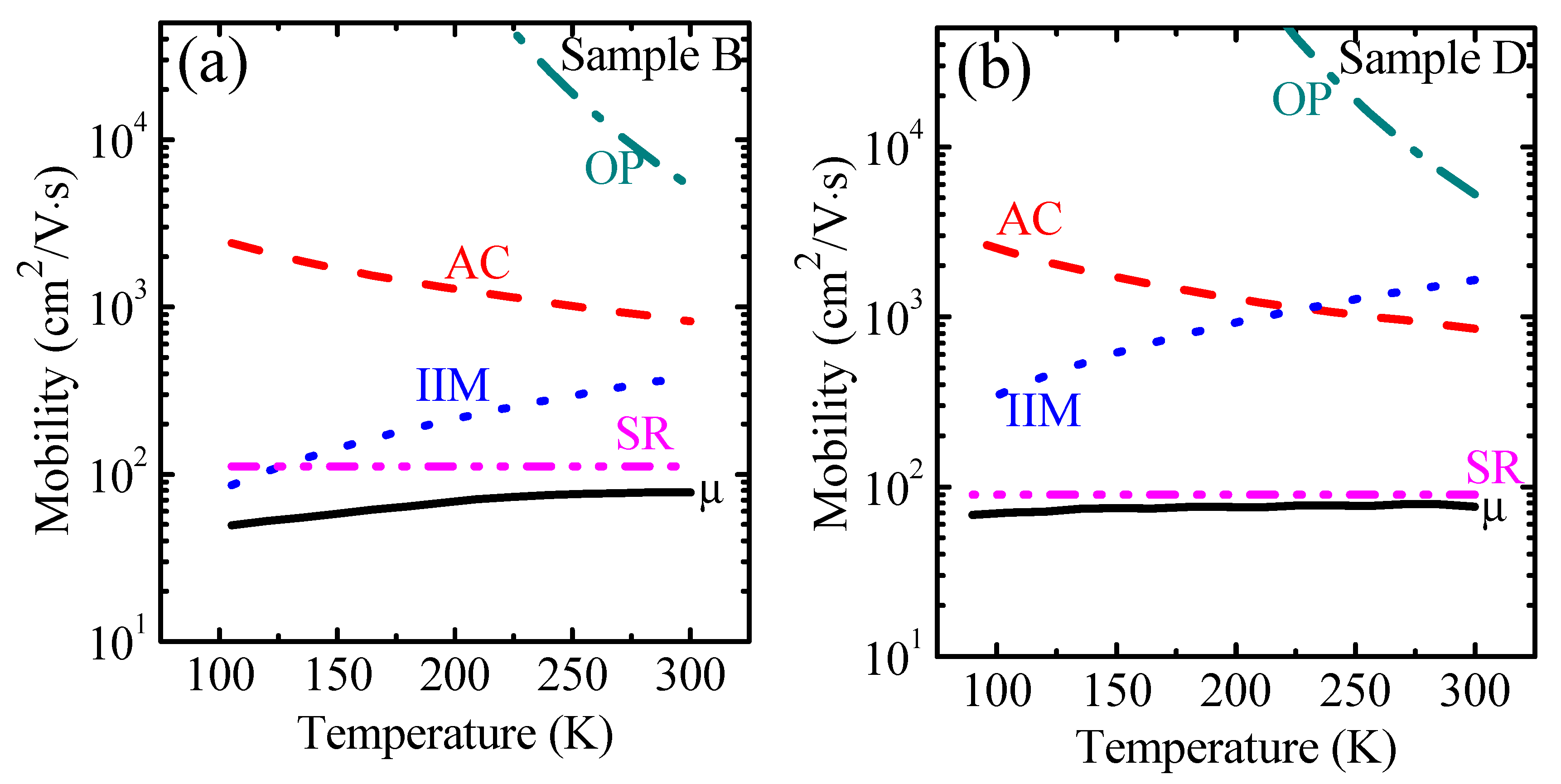
3. Results and Discussion

Figure 1 shows the relationship of carrier mobility μ vs. sheet density NS at room temperature for the three kinds of H-terminated diamond samples. As shown in Figure 1, all the samples follow the µ∝1/Ns relationship, indicating the mobility of the 2DHG in the H-terminated diamond is limited by ionized impurity scattering [22]. The mobility values of the PC-H plasma treatment samples are comparable with the SC-Epitaxial H-termination samples and SC-H plasma treatment samples, showing that the grain boundary scattering is not dominant at this mobility level for the H-terminated diamond. This may be the reason why H-terminated diamond FETs on polycrystalline diamond samples show comparable or even better DC and RF properties than those on single crystal diamond samples [23].
To analyze the carrier transport mechanism of the 2DHG in H-terminated diamond, Van der Pauw–Hall measurements were performed. As listed in Table 1, five samples with (samples A, B, and C) and without (samples C and D) ALD Al2O3 deposition were studied. All the five samples are a single crystal diamond. The ALD processes were performed at 450 °C, 400 °C, and 300 °C for samples A, B, and C, respectively. From Table 1, it can be seen that the carrier mobility μ of the samples A, B, and C decreased after the Al2O3 deposition. The changes of the sheet density Ns of the samples are dependent on the deposition temperatures of the ALD Al2O3, as shown in Figure 2a and Table 1. For sample C with the ALD temperature of 300 °C, the sheet density Ns decreases. For sample B with the ALD temperature of 400 °C, the sheet density Ns shows a small decrease. Additionally, for sample A with the ALD temperature of 450 °C, the sheet density Ns increases. The adsorbates on the H-terminated diamond surface formed in the air desorbed from the surface during the heating process. Additionally, the ALD Al2O3 is the new transfer doping layer for the formation of the 2DHG of the H-terminated diamond. The different changes of sheet density Ns of the samples A, B, and C could be due to the different electron affinities of the ALD of Al2O3 deposited at different temperatures [24]. Hiraiwa et al. found that the Al2O3 electron affinity increases with the increasing of the Al2O3 deposition temperature. The high electron affinity of Al2O3 induces a high sheet density in the H-terminated diamond.
Figure 2b shows the temperature dependences of the sheet resistance Rs of the H-terminated diamond samples with and without the ALD Al2O3. The sheet resistances of all the five samples decrease with temperature, which are due to the carrier mobility increases with temperature, as shown in Figure 2d. The sheet densities of the H-terminated diamond samples keep unchanged or slightly reduced with temperature, as shown in Figure 2c. The weak dependence of sheet density with temperature should be due to the electron affinity difference of the ALD Al2O3 and the H-terminated diamond is almost unchanged in the temperature range from 90 to 300 K. The carrier mobility of all the five samples increases with temperature. The carrier mobility of the H-terminated diamond samples with Al2O3 (samples A, B, and C) shows a stronger temperature dependence compared with those without (w/o) Al2O3 (samples D and E). The temperature dependence of the mobility of the 2DHG is fitted considering four scattering mechanisms to analyze the influences of Al2O3 deposition on the transport properties of the 2DHG in the H-terminated diamond.
The total relaxation time can be obtained by the Mathiessen rule:
1 τ = n 1 τ n
where τn is the momentum relaxation time corresponding to the nth scattering mechanism. The mobility of the 2DHG of the H-terminated diamond can be obtained by the equation μ = e τ / m c * , where m c * is the conduction mass, and formulated as m c * = ( m l h * 3 / 2 + m h h * 3 / 2 + m s o * 3 / 2 ) / ( m l h * 1 / 2 + m h h * 1 / 2 + m s o * 1 / 2 ) [25,26] with m c * = 0.444731 m0. The quantities mhh*, mlh*, and mso* are the heavy, light, and spin-orbit hole mass, respectively.
(1)
Acoustic phonon (AC) scattering
Phonons are the quanta of the lattice vibrations of materials and introduce intrinsic scatterings to carriers. Due to different modes of vibrations, phonons can be divided into acoustic phonons and optical phonons. In this work, the relaxation time limited by the acoustic phonon was calculated following the formula for 2DEG [27]:
1 τ a c = 3 m d * b k B T D a c 2 16 ρ u l 2 3
where ρ is the mass density, kB is the Boltzmann constant, Dac is the acoustic deformation potential, and ul is the longitudinal acoustic phonons velocity. The parameter b =   [ 33 π m d * e 2 p s 2 D / 2 2 ε 0 ε s ] 1 / 3 . In this paper, the acoustic deformation potential was considered as 8 eV. The density of state mass of diamond m d * was evaluated as m d * = ( m l h * 3 / 2 + m h h * 3 / 2 + m s o * 3 / 2 ) 2 / 3 [28] and m d * = 0.907832 m0.
(2)
Optical phonon (OP) scattering
The Debye temperature is about 2240 K for a diamond, which is very high. If the optical phonons dominate the carrier scattering, an exponential drop in carrier mobility with temperature is expected for T < 600 K. The carrier mobility can be estimated by [29]:
μ O P = 4 2 π q ρ 2 k Θ 3 D 0 2 ( m d * ) 3 / 2 m c * φ ( T )
where D0 is the optical deformation potential. φ(T) is a temperature-dependent function, which is in an exponential relationship and drops with temperature T below the Debye temperature.
(3)
Ionic impurity (IM) scattering
Due to its deep impurity levels, the ionized impurity concentration is not a constant for diamond. This makes the ionic impurity scattering momentum relaxation time show a strong temperature dependence. The classical expression for the ionized impurity scattering momentum relaxation time is the Brooks–Herring expression [30]:
τ i m = 16 2 m c * π ε 2 Z 2 q 4 N I ( ln ( 1 + b ) b / ( 1 + b ) ) E 3 / 2
where b = 8 m c * L D 2 E / 2 and ε is the dielectric constant of the medium. NI is the ionized impurity concentration. Z is degree of ionization. LD is the Debye length and E is the carrier energy. Assuming parabolic bands, by averaging over carrier momentum and neglecting the weak dependence of b on energy, the ionized impurity scattering limited relaxation time can be written as:
τ i m = 128 2 π m c * ε 2 ( k T ) 3 2 Z 2 q 4 N I ( ln ( 1 + b ) b / ( 1 + b ) )
where b = 24 m c * L D 2 k T / 2 .
(4)
Surface roughness (SR) scattering
The relaxation time of SR is expressed including the screening by the 2DHG as [31]:
1 τ = 2 L 2 e 4 m d * 2 ε 0 ε s 2 3 ( N s 2 ) 2 · 0 1 u 4 exp ( k F 2 L 2 u 2 ) ( u + G ( q ) q T F / ( 2 k F ) ) 2 1 u 2 d u
where ∆ is the root-mean-square roughness of surface and L is the correlation length. u = q/2kF, which is a dimensionless parameter, with q = 2kFsin(θ/2), θ∈(0, π). θ is the angle between the initial and final wave vector.
Figure 3 shows the fitting results of the carrier mobility of the 2DHG with temperature for samples B and D. It can be seen that the surface roughness (SR) scattering and ionic impurity (IM) scattering are the dominant scattering sources in the measured temperature range. For sample B with Al2O3 deposition, the influence of IM scattering enhances, as shown in Figure 3a. This indicates that the adsorbates on the H-terminated diamond surface formed in the air desorbed from the surface during the heating process of the Al2O3 deposition. The ALD Al2O3 as the new transfer doping layer makes the concentration of the ionized impurity NI increase. This is consistent with the results of Liu et al. [17]. They found that there were negative charges at the Al2O3/H-terminated diamond interface. They thought the unoccupied levels within the Al2O3 dielectric near the Al2O3/H-terminated diamond interface were the main sources of the negatively charged acceptors at the Al2O3/H-terminated diamond interface. The above results indicate that the initial stage of the ALD Al2O3 is especially important for the H-terminated diamond. The reduction of unoccupied levels in the Al2O3 near the Al2O3/H-terminated diamond interface will be beneficial for the carrier mobility improvement of the 2DHG in the H-terminated diamond.

4. Conclusions

In summary, we studied the influence of Al2O3 deposition by a high-temperature atomic layer deposition process on the transport properties of the 2DHG in a H-terminated diamond. The temperature dependence of the mobility of the 2DHG is fitted considering four scattering mechanisms: ionic impurity scattering, acoustic phonon scattering, optical phonon scattering and surface roughness scattering. The surface roughness scattering and ionic impurity scattering are found to be the dominant scattering sources in the H-terminated diamond. Impurity scattering enhancement was found for the H-terminated diamond sample after the high-temperature atomic layer deposition Al2O3 process.

Author Contributions

Conceptualization, C.Y.; validation, Z.F., A.B.; formal analysis, C.Y.; investigation, C.Z., J.G., M.M. and H.W.; resources, C.Y.; data curation, C.Y. and Z.F.; writing—original draft preparation, C.Y.; writing—review and editing, C.Y.; visualization, C.Y.; supervision, Z.F. and A.B.; project administration, C.Y. and Z.H.; funding acquisition, C.Y. All authors have read and agreed to the published version of the manuscript.

Funding

National Key R&D Program of China, National Natural Science Foundation of the Hebei Province, and National Key Science and Technology Special Project.

Institutional Review Board Statement

Not applicable.

Informed Consent Statement

Not applicable.

Data Availability Statement

Not applicable.

Acknowledgments

This work was financially supported by the National Key R&D Program of China (Grant No. 2018YFE0125900), the National Natural Science Foundation of the Hebei Province (Grant No. F2019516002), and the National Key Science and Technology Special Project (Grant No. 2009ZYHW0015).

Conflicts of Interest

The authors declare no conflict of interest.

References

  1. Wort, C.J.H.; Balmer, R.S. Diamond as an electronic material. Mater. Today 2008, 11, 22. [Google Scholar] [CrossRef]
  2. Hui, J.L.; Pang, L.Y.S.; Molloy, A.B.; Jones, F.; Whitfield, M.D.; Foord, J.S.; Richard, B.J. Mechanisms of surface conductivity in thin film diamond: Application to high performance devices. Carbon 1999, 37, 801. [Google Scholar]
  3. Kawarada, H.; Aoki, M.; Ito, M. Enhancement mode metal-semiconductor field effect transistors using homoepitaxial diamonds. Appl. Phys. Lett. 1994, 65, 1563. [Google Scholar] [CrossRef]
  4. Williams, O.A.; Jackman, R.B. High growth rate MWPECVD of single crystal diamond. Diam. Relat. Mater. 2004, 13, 325. [Google Scholar] [CrossRef]
  5. Looi, H.J.; Pang, L.Y.S.; Molloy, A.B.; Jones, F.; Foord, J.S.; Jackman, R.B. An insight into the mechanism of surface conductivity in thin film diamond. Diam. Relat. Mater. 1998, 7, 550. [Google Scholar] [CrossRef]
  6. Jiang, N.; Ho, T. Electrical properties of surface conductive layers of homoepitaxial diamond films. J. Appl. Phys. 1999, 85, 8267. [Google Scholar] [CrossRef]
  7. Hirama, K.; Sato, H.; Harada, Y.; Yamamoto, H.; Kasu, M. Diamond Field-Effect Transistors with 1.3 A/mm Drain Current Density by Al2O3 Passivation Layer. Jpn. J. Appl. Phys. 2012, 51, 090112. [Google Scholar]
  8. Ueda, K.; Kasu, M.; Yamauchi, Y.; Makimoto, T.; Schwitters, M.; Twitchen, D.J.; Scarsbrook, G.A.; Coe, S.E. Diamond FET using high-quality polycrystalline diamond with fT of 45 GHz and fmax of 120 GHz. IEEE Electron. Device Lett. 2006, 27, 57. [Google Scholar] [CrossRef]
  9. Imanishi, S.; Horikawa, K.; Oi, N.; Okubo, S.; Kageura, T.; Hiraiwa, A.; Kawarada, H. 3.8 W/mm RF Power Density for ALD Al2O3-Based Two-Dimensional Hole Gas Diamond MOSFET Operating at Saturation Velocity. IEEE Electron. Device Lett. 2018, 40, 279–281. [Google Scholar] [CrossRef]
  10. Zhou, C.J.; Wang, J.J.; Guo, J.C.; Yu, C.; He, Z.Z.; Liu, Q.B.; Gao, X.D.; Cai, S.J.; Feng, Z.H. Radiofrequency performance of hydrogenated diamond MOSFETs with alumina. Appl. Phys. Lett. 2019, 114, 063501. [Google Scholar] [CrossRef]
  11. Yu, C.; Zhou, C.J.; Guo, J.C.; He, Z.Z.; Wang, H.X.; Cai, S.J.; Feng, Z.H. 650 mW/mm output power density of H-terminated polycrystalline diamond MISFET at 10 GHz. Electron. Lett. 2020, 56, 334–335. [Google Scholar] [CrossRef]
  12. Kawarada, H.; Yamada, T.; Xu, D.; Kitabayashi, Y.; Shibata, M.; Matsumura, D.; Kobayashi, M.; Saito, T.; Kudo, T.; Inaba, M.; et al. Diamond MOSFETs using 2D Hole Gas with 1700V Breakdown Voltage. In Proceedings of the 28th ISPSD, Prague, Czech Republic, 12–16 June 2016; p. 483. [Google Scholar]
  13. Ghasemi, M.H.; Abouei, V.; Moshtaghi, M.; Noghani, M.T. The effect of removing worn particles by ultrasonic cleaning on the wear characterization of LM13 alloy. Surf. Eng. Appl. Electrochem. 2015, 51, 382–388. [Google Scholar] [CrossRef]
  14. Masafumi, K.; Ishii, H.; Shirai, Y.; Ohmi, T. High-corrosion-resistance Al2O3 passivation-film formation by selective oxidation on austenitic stainless steel containing Al. J. Vac. Sci. Technol. A Vac. Surf. Film. 2011, 29, 021002. [Google Scholar]
  15. Hiraiwa, A.; Daicho, A.; Kurihara, S.; Yokoyama, Y.; Kawarada, H. Refractory two-dimensional hole gas on hydrogenated diamond surface. J. Appl. Phys. 2012, 112, 124504. [Google Scholar]
  16. Ren, Z.; Lv, D.; Xu, J.; Zhang, J.; Zhang, J.; Su, K.; Zhang, C.; Hao, Y. High temperature (300 °C) ALD grown Al2O3 on hydrogen terminated diamond: Band offset and electrical properties of the MOSFETs. Appl. Phys. Lett. 2020, 116, 013503. [Google Scholar] [CrossRef]
  17. Liu, J.W.; Oosato, H.; Da, B.; Koide, Y. Fixed charges investigation in Al2O3/hydrogenated-diamond metal-oxide semiconductor capacitors. Appl. Phys. Lett. 2020, 117, 163502. [Google Scholar] [CrossRef]
  18. Sasama, Y.; Kageura, T.; Komatsu, K.; Moriyama, S.; Inoue, J.; Imura, M.; Watanabe, K.; Taniguchi, T.; Uchihashi, T.; Takahide, Y. Charge-carrier mobility in hydrogen-terminated diamond field-effect transistors. J. Appl. Phys. 2020, 127, 185707. [Google Scholar] [CrossRef]
  19. Li, Y.; Zhang, J.F.; Liu, G.P.; Ren, Z.Y.; Zhang, J.C.; Hao, Y. Mobility of two-dimensional hole gas in H-terminated diamond. Phys. Status Solidi (RRL) 2018, 12, 1700401. [Google Scholar] [CrossRef]
  20. Wang, J.J.; He, Z.Z.; Yu, C.; Song, X.B.; Wang, H.X.; Lin, F.; Feng, Z.H. Comparison of field-effect transistors on polycrystalline and single-crystal diamonds. Diam. Relat. Mater. 2016, 70, 114–117. [Google Scholar] [CrossRef]
  21. Wang, J.J.; He, Z.Z.; Yu, C.; Song, X.B.; Xu, P.; Zhang, P.W.; Guo, H.; Liu, J.L.; Li, C.M.; Cai, S.J.; et al. Rapid deposition of polycrystalline diamond film by DC arc plasma jet technique and its RF MESFETs. Diam. Relat. Mater. 2014, 43, 43–48. [Google Scholar] [CrossRef]
  22. Koizumi, S.; Nebel, C.; Nesladek, M. (Eds.) Physics and Applications of CVD Diamond; John Wiley & Sons: Hoboken, NJ, USA, 2008. [Google Scholar]
  23. Camarchia, V.; Cappelluti, F.; Ghione, G.; Limiti, E.; Moran, D.A.J.; Pirola, M. An overview on recent developments in RF and microwave power H-terminated diamond MESFET technology. In Proceedings of the 2014 International Workshop on Integrated Nonlinear Microwave and Millimetre-Wave Circuits (INMMiC), Leuven, Belgium, 2–4 April 2014; IEEE: New York, NY, USA, 2014. ISBN 978-1-4799-3454-6/14/. [Google Scholar]
  24. Hiraiwa, A.; Matsumura, D.; Kawarada, H. Effect of atomic layer deposition temperature on current conduction in Al2O3 films formed using H2O oxidant. J. Appl. Phys. 2016, 120, 084504. [Google Scholar]
  25. Tsukioka, K.; Okushi, H. Hall mobility and scattering mechanism of holes in boron-doped homoepitaxial chemical vapor deposition diamond thin films. Jpn. J. Appl. Phys. 2006, 45, 8571. [Google Scholar] [CrossRef]
  26. Tsukioka, K. Scattering mechanisms of carriers in natural diamond. Jpn. J. Appl. Phys. 2001, 40, 3108. [Google Scholar] [CrossRef]
  27. Davies, J.H. The Physics of Low-Dimensional Semiconductors: An Introduction; Cambridge University Press: Cambridge, UK, 1998; p. 365. [Google Scholar]
  28. Pernot, J.; Volpe, P.N.; Omnès, F.; Muret, P.; Mortet, V.; Haenen, K.; Teraji, T. Hall hole mobility in boron-doped homoepitaxial diamond. Phys. Rev. B 2010, 81, 205203. [Google Scholar] [CrossRef]
  29. Sussmann, R.S. CVD Diamond for Electronic Devices and Sensors; John Wiley & Sons, Ltd.: Hoboken, NJ, USA, 2009; ISBN 978-0-470-06532-7. [Google Scholar]
  30. Brooks, H. Advances in Electronics and Electron Physics; Marton, L., Ed.; Academic Press: New York, NY, USA, 1955; p. 158. [Google Scholar]
  31. Zanato, D.; Gokden, S.; Balkan, N.; Ridley, B.K.; Schaff, W.J. The effect of interface-roughness and dislocation scattering on low temperature mobility of 2D electron gas in GaN/AlGaN. Semicond. Sci. Technol. 2004, 19, 427. [Google Scholar] [CrossRef]
Figure 1. Relationship of carrier mobility μ vs. sheet density NS at room temperature for the H-terminated diamond samples.
Crystals 12 00390 g001
Figure 2. The electrical properties of the five H-terminated diamond samples with (samples A, B, and C) and without (samples D and E) ALD Al2O3. (a) Change of sheet density Ns of the samples A, B, and C vs. performed temperatures of ALD processes. Temperature dependences of (b) sheet resistance, (c) sheet density, and (d) carrier mobility for the H-terminated diamond samples with and without ALD Al2O3.
Crystals 12 00390 g002
Figure 3. The fitting of carrier mobility as a function of temperature. (a) Sample B. (b) Sample D. AC represents the acoustic deformation potential scattering; OP is the nonpolar optical phonon scattering; SR is the interface roughness scattering; IM is the surface impurity scattering; and μ denotes the resulting 2DHG mobility covering the above four scattering mechanisms.
Crystals 12 00390 g003
Table 1. Room temperature electrical properties of five H-terminated single crystal diamond samples with and without Al2O3 deposition.
Sample NameBefore Al2O3 DepositionAfter Al2O3 DepositionAl2O3 Deposition Temperature (°C)
Rs (Ω/sq)Ns (1012/cm2)μ (cm2/V·s)Rs (Ω/sq)Ns (1012/cm2)μ (cm2/V·s)
A87274.71515273606.18137450
B92716.46110413,300677.9400
C83327.51299.711,5005.37101300
D700011.776.4——-
E538014.380.9——-
Publisher’s Note: MDPI stays neutral with regard to jurisdictional claims in published maps and institutional affiliations.

