Article

Reduction in the Photoluminescence Intensity Caused by Ultrathin GaN Quantum Barriers in InGaN/GaN Multiple Quantum Wells

1
School of Microelectronics, Northwestern Polytechnical University, Xi’an 710072, China
2
State Key Laboratory of Integrated Optoelectronics, Institute of Semiconductors, University of Chinese Academy of Sciences, Beijing 100083, China
3
Center of Materials Science and Optoelectronics Engineering, University of Chinese Academy of Sciences, Beijing 100049, China
*
Authors to whom correspondence should be addressed.
Crystals 2022, 12(3), 339; https://doi.org/10.3390/cryst12030339
Submission received: 9 January 2022 / Revised: 24 February 2022 / Accepted: 26 February 2022 / Published: 28 February 2022
(This article belongs to the Special Issue Advances in GaN-Based Optoelectronic Materials and Devices)

Abstract

:
The optical properties of InGaN/GaN violet light-emitting multiple quantum wells with different thicknesses of GaN quantum barriers are investigated experimentally. When the barrier thickness decreases from 20 to 10 nm, the photoluminescence intensity at room temperature increases, which can be attributed to the reduced polarization field in the thin-barrier sample. However, with a further reduction in the thickness to 5 nm, the sample’s luminescence intensity decreases significantly. It is found that the strong nonradiative loss process induced by the deteriorated crystal quality and the quantum-tunneling-assisted leakage of carriers may jointly contribute to the enhanced nonradiative loss of photogenerated electrons and holes, leading to a significant reduction in photoluminescence intensity of the sample with nanoscale ultrathin GaN quantum barriers.

1. Introduction

Group III–nitride materials have garnered significant attention in the research field of compound-semiconductor electronics and optoelectronics due to their large direct bandgap and other excellent physical properties [1,2,3,4,5,6,7,8]. In particular, the photoelectric characteristics of InGaN/GaN multiple quantum wells (MQWs) have been investigated intensively, as they are widely used as the active materials of light-emitting devices for the applications of white-light illumination and color display [9,10,11,12,13]. In general, the InGaN well layers are considered the pivotal factor in determining the luminescence properties of InGaN/GaN MQWs, since the nonequilibrium electrons and holes mainly recombine radiatively and emit photons in InGaN QWs. Due to the growth of InGaN/GaN MQWs along the polar GaN [0001] direction, in InGaN QWs the polarization-induced quantum-confined Stark effect (QCSE), reducing the luminescence efficiency of InGaN QWs as well as the energy of emitted photons, plays a crucial role in the luminescence characteristics of light-emitting devices, which has attracted high research interest [14,15,16]. Nevertheless, the GaN quantum barriers also affect the QCSE in InGaN QWs as well as the transport of carriers in the whole MQW active region, which may strongly influence the performance of the optoelectronic devices based on the InGaN/GaN MQWs [17,18]. Compared with blue and green light-emitting InGaN/GaN MQWs, in the violet ones the In composition in InGaN well layers is smaller; accordingly, the effective potential height of the GaN barriers is reduced, resulting in a more significant influence of GaN barriers on the characteristics of violet MQW-based devices [19,20]. Therefore, the structural parameters of GaN barrier layers should be investigated carefully for the violet light-emitting InGaN/GaN MQWs.
In this paper, we focus on the effects of the GaN barrier thickness on the luminescence properties of violet InGaN/GaN MQWs. Since the influence of different barrier thicknesses on the MQW optical properties is significantly different, the MQW samples with 20-nm ultrathick and 5-nm ultrathin barriers are studied together here in order to reveal the barrier thickness-related physical mechanisms in the violet InGaN/GaN MQWs deeply and comprehensively. It is demonstrated that the light-emission efficiency of MQWs with ultrathin GaN barriers can be reduced seriously due to the enhanced nonradiative recombination process. The material quality, epitaxial growth process, and related luminescence mechanisms are discussed in detail later.

2. Materials and Methods

InGaN/GaN MQW samples S1, S2, and S3 were grown on c-plane sapphire substrates by the AIXTRON close-coupled showerhead 3 × 2 in. vertical reactor metal–organic chemical vapor deposition (MOCVD) system. For each sample, there were three pairs of InGaN wells and GaN barriers, which were sandwiched between a 2 μm-thick GaN template layer and a 150 nm-thick GaN cap layer, i.e., there are a total of 3 MQW samples, and each of them has 3 InGaN QWs in our experiment. During the epitaxial growth of the MQW layers, the growth temperature of the InGaN well layers was 690 °C; then, it was ramped up to 860 °C for the successive growth of the GaN barrier layers. The higher growth temperature of the GaN layers was used to improve the crystal quality of GaN materials. The epitaxial structures of all samples were exactly the same, except for the thickness of the GaN barriers in the MQW layers, which was intentionally adjusted by changing the growth time of the GaN layers. The growth conditions and structural parameters were calibrated by transmission electron microscope and X-ray diffraction measurement, previously [21]. Therefore, based on the calibration data, in the InGaN QW layers the nominal In content was set to be 8%, and the layer thickness was 2.5 nm for all samples. The thicknesses of the GaN barrier layers of samples S1, S2, and S3 were about 20, 10 and 5 nm, respectively.
The luminescence properties of all samples were investigated by temperature-dependent photoluminescence (TDPL) measurements, where the 1K3301R-G 325-nm continuous wave He–Cd laser, manufactured by Kimmon Koha Co., Ltd. in Tokyo, Japan, was used as a constant excitation source, and the temperatures were controlled from 30 to 300 K by the MODEL 22 closed-cycle helium refrigerator of CTI Cryogenics. The accurate peak energy and integrated PL intensity of the detected spectra of all samples were fitted by a Gaussian function to eliminate the influence induced by the Fabry-Perot interference fringes [22]. The high-resolution X-ray diffraction (HRXRD) ω/2θ scan and reciprocal space mapping (RSM) were performed to determine the MQW structural parameters and material quality by using Rigaku Ultima IV X-ray diffractometer with Cu-1 radiation (λ = 1.54 Å) manufactured by Rigaku Corporation in Tokyo, Japan.

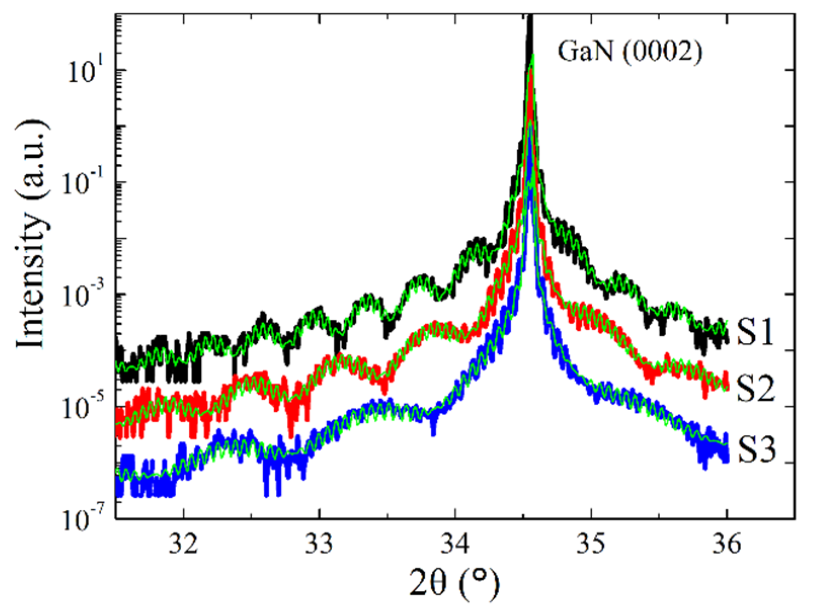
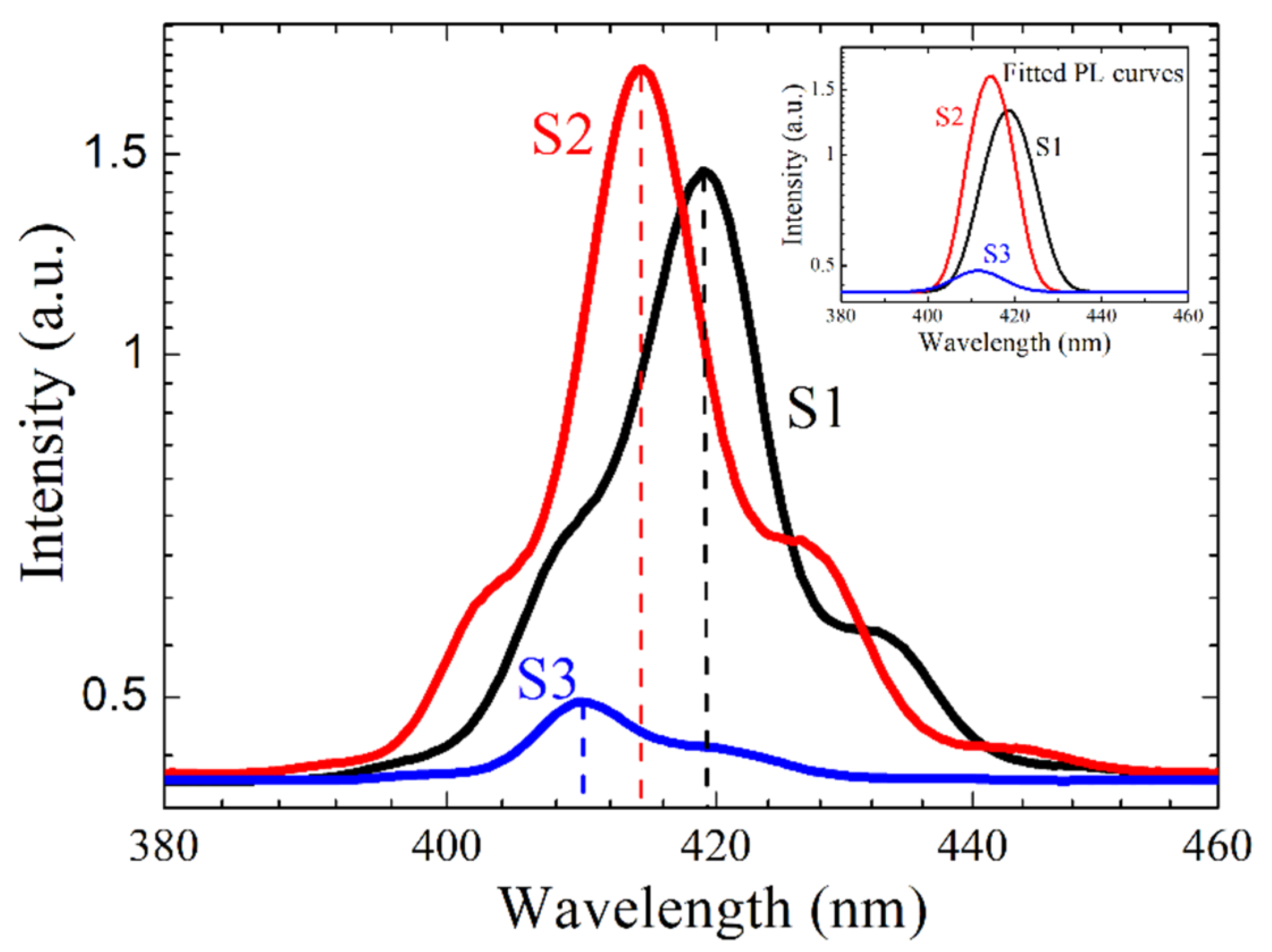
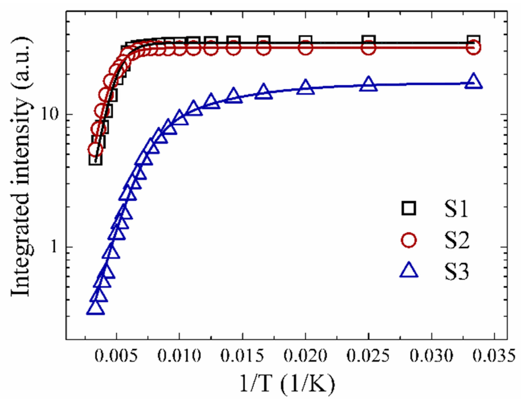
3. Results and Discussion

The HRXRD (0002) ω/2θ scan curves of three samples are depicted in Figure 1, where the scan curves of samples S1 and S2 are vertically shifted for clarity. The strong main peaks and several weak satellite peaks can be seen for all samples, which originate mainly from the underlying c-plan GaN layers and the InGaN/GaN MQW layers, respectively. The presence of satellite peaks clearly indicates that a well-defined MQW periodic structure was formed. The MQW structural parameters were obtained via fitting the measured HRXRD ω/2θ curves using the GlobalFit simulation program embedded in the operation software package of the Rigaku X-ray diffractometer, where the Vickers’s method was adopted [23]. The fitted ω/2θ curves of all samples were directly superimposed on their measured ones. It is clear that all samples’ measured results can be well fitted by the simulated curves, meaning that the simulated structural parameters of the InGaN/GaN MQWs are consistent with the actual ones. According to the fitted results, the GaN barrier thickness, the InGaN well thickness, and the average In content in sample S1 were 20.8 nm, 2.5 nm, and 7.5%, respectively. They were 11.5 nm, 2.5 nm, and 8.2% for sample S2, and 5.4 nm, 2.4 nm, and 8.3% for S3, respectively. There was an approximately 10% difference between the designed and measured structural parameters, which is a typical magnitude of variation in determining the structural parameters of InGaN/GaN MQWs by X-ray diffraction [24]. Thus, it was confirmed that the grown MQW samples were basically consistent with our designed structural parameters.
Figure 2 shows the PL spectra of all MQW samples at room temperature. Although the structural parameters of the InGaN QWs were identical for all three samples, the peak wavelengths of S1, S2, and S3 were 419, 414, and 410 nm, respectively. The reduction in peak wavelength with decreasing barrier thickness indicates that the QCSE induced by the polarization field in QWs was weakened for the thin-barrier sample. In fact, it is theoretically known that in the periodic InGaN/GaN MQW structure the polarization-induced electric field in QWs is closely related to the structural parameters of both the InGaN well and GaN barrier layers [25]. Similar to the effect of reducing the InGaN QW thickness on the QCSE, when the thickness of the GaN barrier layer decreased, the polarization-induced electric field in InGaN QWs was reduced, i.e., the QCSE was weaker for the samples with thinner GaN barrier layers. Therefore, the PL spectra blue-shifted monotonically with decreasing barrier thickness, as shown in Figure 2. On the other hand, it is noted that the samples’ PL intensities increased first and then decreased, when the GaN barrier thickness decreased from samples S1 to S3. The enhanced PL intensity of sample S2 can be ascribed to the weaker QCSE due to the reduced barrier thickness. However, it is surprising that the PL intensity of sample S3 was much smaller than those of other two samples, although the QCSE was the weakest in sample S3.
To explore the reason responsible for the significantly reduced PL intensity of sample S3, the dependence of the samples’ integrated PL intensities on the reciprocal temperatures are plotted in Figure 3, where the thermal decay of PL intensity can be seen for all samples. It is well known that the reduction in PL intensity with increasing temperature can be attributed to the thermally activated nonradiative recombination process. It is seen in Figure 3 that the thermal decay behaviors of samples S1 and S2 were similar to each other, implying that the nonradiative recombination processes in these two samples were almost the same. It should be noticed that at low temperatures the integrated PL intensity of sample S1 was a little larger than that of sample S2, which was contrary to the comparison of their PL spectra at room temperature in Figure 2. In fact, the nonequilibrium electrons and holes can also be generated in the GaN barrier layers, as the photon energy of the excitation source of 325-nm laser used in our PL measurement was larger than the bandgap of GaN materials. Thus, more carriers can be generated in the thicker GaN barriers and then injected into the InGaN QWs. Therefore, compared with sample S2, the stronger PL intensity of S1 at a low temperature may be ascribed to the increased photogenerated carriers contributed by the thicker GaN barrier layers [26]. However, at room temperature, the nonradiative recombination process dominated in InGaN QWs, and the nonradiative loss of carriers was more serious for sample S1 than for S2 due to the enhanced QCSE by the thicker barriers of sample S1. Thus, at room temperature the PL intensity of S1 was smaller than that of S2, even though more carriers generated in thicker GaN barriers may be injected into the InGaN QWs for sample S1.
For sample S3, it is obvious that the PL intensities were much weaker in the entire temperature range, and the thermal decay behavior of the integrated PL intensity differed from the other two samples, implying that the nonradiative recombination process in S3 may be different from the others. Generally, the thermal decay curves of integrated intensity can be described by the Arrhenius relationship in Equation (1), following [27]:
I ( T ) = I 0 1 + i C i exp ( E i / k B T )
where I0 is the integrated PL intensity at low temperature. Ci is related to the density of nonradiative recombination centers, Ei is the activation energy of the corresponding nonradiative recombination process accounting for the thermal decay of PL intensity, and kB is the Boltzmann’s constant. The subscript i indicates the number of nonradiative channels. The value of i can be larger than 1, if there is more than one nonradiative recombination channel. Among the fitted parameters, the activation energy Ei is the key parameter at which the corresponding nonradiative process can be thermally activated. Normally, Ei can be related to the thermal ionization energy of the nonradiative centers causing the nonradiative recombination process. The smaller value of Ei implies that the nonradiative process can be activated at a lower thermal energy, i.e., a lower temperature. It was found that the temperature-dependent behaviors of the integrated PL intensities of samples S1 and S2 could be fitted well by assuming one dominant nonradiative channel. However, the experimental data of sample S3 could only be well described by the Arrhenius equation with two nonradiative channels, as illustrated in Figure 3. This means that only one major nonradiative recombination process predominated the loss of carriers in samples S1 and S2, but there were two nonradiative channels responsible for the carrier loss in sample S3, as the temperature increased. Table 1 shows the fitted values of the Arrhenius parameters for all samples.
It is reasonable to assume that the first nonradiative channel could be ascribed to the conventional thermal decay process induced by the thermally activated nonradiative recombination centers, which often originate from the point or extended crystal defects in InGaN alloys [28]. Generally, the thermal activation energy E1 of the first nonradiative channel is determined by the nonradiative capturing process of charge carriers, which is closely related to the concentration, types, and characteristics of crystal defects [29]. Thus, this indicates that there was no significant difference in the defects-related nonradiative processes between samples S1 and S2, since the values of E1 were almost the same for both samples, as seen in Table 1. However, it is noted that the activation energy E1 of sample S3 was only 70.6 meV, which was much smaller than those of other two samples. In general, in the InGaN alloys with poor crystal quality, the value of E1 can be reduced significantly due to the increased concentration of, or even types of, defects. Therefore, after comparing the thermal activation energies of all samples, this may indicate that the defect-related nonradiative recombination process was more significant in sample S3 than in S1 and S2, which may be attributed to the deteriorated crystal quality of sample S3.
Therefore, the material quality of the InGaN/GaN MQWs was then assessed by the RSM around the (105) reflection for all samples, as depicted in Figure 4. For the XRD RSM measurement of III-nitride, the (105) direction is frequently used to obtain the information regarding the biaxial strain state as well as the material quality [30]. The numbers of observed reflections corresponding to the MQW satellite peaks were 3, 2, and 1 for samples S1, S2 and S3, respectively. This means that the separation distance between the adjacent reflections was increased. It is known that for the RSM measurement the separation distance between the adjacent satellite peaks increases with a decrease in the thickness of one MQW period, i.e., the thickness of the well layer plus the barrier layer [30]. Therefore, the reduced number of observed reflection peaks from samples S1 to S3 can be attributed to the decreased MQW period due to the reduced GaN barrier thickness. For samples S1 and S2, the reflection peaks corresponding to the GaN layers and to the MQWs were vertically aligned (same in-plane wave vector Qx), meaning that the growth of the MQW layers was fully strained on the GaN template layer. Thus, it is reasonable to consider that the crystal quality of samples S1 and S2 was almost identical, and correspondingly, the defect-related nonradiative recombination processes in both samples were similar, which is consistent with the comparison of the fitted values of the thermal activation energy E1 of samples S1 and S2 in Table 1.
However, for sample S3, there was a small but detectable in-plane lateral shift of the MQW satellite peaks with respect to the GaN template peak, indicating that a small partial relaxation of the in-plane coherency strain occurred in the MQW layers. According to the extent of the lateral shift of MQW peaks, the degree of strain relaxation of the InGaN well layers in sample S3 can be calculated to be about 9.7% [31]. This implies that more crystal defects, such as misfit dislocations, may appear at the interface of the InGaN/GaN heterostructure, i.e., compared with other two samples, the quality of the MQW materials was deteriorated for S3. This may be the reason why the fitted activation energy E1 of sample S3 was much smaller than those of the other two samples in Table 1, since the increased defects acting as nonradiative recombination centers can capture a larger number of photogenerated carriers and enhance the nonradiative recombination process in InGaN alloy with poor crystal quality [29]. As a result, a remarkable nonradiative loss of nonequilibrium carriers occurred in the MQW active region, leading to a serious reduction in PL intensity of sample S3, as shown in Figure 2.
As mentioned in the experimental section, the growth temperature of the GaN barrier layers was higher than that of the InGaN well layers to enhance the crystal quality of GaN materials. In fact, from another perspective, the process of the high-temperature growth of the GaN barriers can be treated as an annealing process of the InGaN well materials [32]. It is commonly known that the annealing process is widely utilized to improve the crystal quality of semiconductor materials by eliminating the crystal defects. Therefore, the longer growth time of the GaN barriers is equivalent to a longer annealing process of the InGaN well layers, which may be beneficial to improving the crystal quality of InGaN materials, e.g., for samples S1 and S2. On the contrary, for sample S3 with thin GaN barriers, the annealing process for InGaN layers was short due to the reduced growth time of the GaN barriers. As a consequence, the material quality of the InGaN active layers was deteriorated and more crystal defects may exist, leading to the enhanced nonradiative recombination process and the reduction in PL intensity for the ultrathin-barrier sample S3.
In addition, it is noticed in Table 1 that there was an additional nonradiative recombination channel with a much smaller thermal activation energy E2 of 15 meV for sample S3. According to the physical implication of thermal activation energy, the small activation energy means that the nonradiative recombination process can be activated at a very low temperature [33]. On the other hand, according to the basic theory of quantum mechanics, for the quantum tunneling effect, it is well known that thinner quantum barriers provide higher tunneling rates, i.e., the tunneling effect is enhanced in the InGaN/GaN MQW sample with ultrathin GaN barriers [34,35].
Therefore, it is theoretically reasonable that the additional nonradiative channel may originate from the quantum tunneling of carriers, which is less sensitive to the temperature and may even occur at very low temperatures [36], since the thickness of the GaN barriers of sample S3 was as thin as 5 nm. The enhanced tunneling effect may cause a significant leakage of carriers outside from the InGaN QWs, leading to a nonradiative loss of carriers with a much smaller thermal activation energy. Thus, with the combination of the enhanced nonradiative recombination process induced by the deteriorated crystal quality and the remarkable carrier leakage caused by the thin-barrier-induced quantum tunneling effect, most of the nonequilibrium carriers in InGaN QWs were lost, leading to a significant reduction in PL intensity for sample S3 with its ultrathin barrier.
Finally, one should keep in mind that a complete PL process should include the thermionic emission and recapture of carriers in InGaN QWs, which are closely related to the QW depth [37]. For the InGaN/GaN MQWs, not only the In content in InGaN alloy but also the thickness of the InGaN well layer can impact the QW depth due to the polarization effect. Taking sample S1 for example, according to the structural parameters obtained from the HRXRD (0002) ω/2θ scan, the In content in sample S1 was a little smaller, making the QW depth slightly reduced. However, since the measured thickness of the InGaN QW for sample S1 was relatively large, the polarization effect may be promoted; accordingly, the potential well became deeper. As a result, the reduced QW depth induced by a smaller In content may be offset by the increased QW depth caused by the thicker well layer. In fact, in our work, the difference of the potential well depths between different samples can be neglected, as the structural parameters of the InGaN well layers were almost the same for all samples. Therefore, to avoid complication, the discussion on the thermionic emission and recapture of charge carriers was ignored in our manuscript.

4. Conclusions

In summary, the luminescence characteristics and material quality of three InGaN/GaN MQW samples with different GaN barrier layer thicknesses were investigated by TDPL and XRD measurements. It was found that the room-temperature PL intensity increased from sample S1 to S2 and then decreased remarkably for sample S3. The improved light-emission efficiency of S2 can be attributed to the weaker QCSE in the thinner-barrier MQWs, while the significant decrease in PL intensity of sample S3 may be ascribed to the combined effects of the enhanced nonradiative recombination process and the quantum tunneling effect in the ultrathin-GaN-barrier sample.

Author Contributions

Conceptualization, W.L.; formal analysis, W.L. and F.L.; funding acquisition, W.L. and D.Z.; investigation, W.L., J.Y. and Z.L.; supervision, D.Z.; validation, F.L. and P.C.; writing—original draft, W.L.; writing—review and editing, W.L. and F.L. All authors have read and agreed to the published version of the manuscript.

Funding

This research was funded by the National Key R&D Program of China, grant number 2021YFF0307403; the National Natural Science Foundation of China, grant numbers 62074129, 62034008, 62074142, 62074140, 61974162, 61904172, 61874175; the Beijing Nova Program grant number 202093; the Youth Innovation Promotion Association of Chinese Academy of Sciences, grant number 2019115; and the Young Elite Scientists Sponsorship Program by CAST.

Institutional Review Board Statement

Not applicable.

Informed Consent Statement

Not applicable.

Data Availability Statement

Data are available upon request.

Conflicts of Interest

The authors declare no conflict of interest. The funders had no role in the design of the study; in the collection, analyses, or interpretation of data; in the writing of the manuscript, or in the decision to publish the results.

References

  1. Kim, J.; Kim, J.; Oh, S.; Choi, J.; Lee, D.H.; Cho, K.; Lee, S.; Ahn, C.H. A 20-W wide bandwidth GaN HEMT power amplifier for VHF/UHF applications. IEEE Trans. Ind. Electron. 2020, 67, 10905–10910. [Google Scholar] [CrossRef]
  2. Menani, A.; Dehimi, L.; Dehimi, S.; Pezzimenti, F. Modelling and optical response of a compressive-strained AlGaN/GaN quantum well laser diode. J. Semicond. 2020, 41, 062301. [Google Scholar] [CrossRef]
  3. Polyakov, A.Y.; Haller, C.; Butte, R.; Smirnov, N.B.; Alexanyan, L.A.; Shikoh, A.S.; Shchemerov, I.V.; Chernykh, S.V.; Lagov, P.B.; Pavlov, Y.S.; et al. Effects of 5 MeV electron irradiation on deep traps and electroluminescence from near-UV InGaN/GaN single quantum well light-emitting diodes with and without InAlN superlattice underlayer. J. Phys. D Appl. Phys. 2020, 53, 445111. [Google Scholar] [CrossRef]
  4. Li, D.B.; Jiang, K.; Sun, X.J.; Guo, C.L. AlGaN photonics: Recent advances in materials and ultraviolet devices. Adv. Opt. Photonics. 2018, 10, 43–110. [Google Scholar] [CrossRef]
  5. Zhao, D.G. III-nitride based ultraviolet laser diodes. J. Semicond. 2019, 40, 120402. [Google Scholar] [CrossRef]
  6. Jorge, A.; Holguin-Lerma, J.A.; Kong, M.W.; Alkhazragi, O.; Sun, X.B.; Ng, T.K.; Ooi, B.S. 480-nm distributed-feedback InGaN laser diode for 10.5-Gbit/s visible-light communication. Opt. Lett. 2020, 45, 742–745. [Google Scholar]
  7. Li, X.D.; Geens, K.; Amirifar, N.; Zhao, M.; You, S.Z.; Posthuma, N.; Liang, H.; Groeseneken, G.; Decoutere, S. Integration of GaN analog building blocks on p-GaN wafers for GaN ICs. J. Semicond. 2021, 42, 024103. [Google Scholar] [CrossRef]
  8. Cai, X.L.; Du, C.L.; Sun, Z.X.; Ye, R.; Liu, H.J.; Zhang, Y.; Duan, X.Y.; Lu, H. Recent progress of physical failure analysis of GaN HEMTs. J. Semicond. 2021, 42, 051801. [Google Scholar] [CrossRef]
  9. Chen, S.W.; Huang, Y.M.; Singh, K.J.; Hsu, Y.C.; Liou, F.J.; Song, J.; Choi, J.; Lee, P.T.; Lin, C.C.; Chen, Z.; et al. Full-color micro-LED display with high color stability using semipolar (20-21) InGaN LEDs and quantum-dot photoresist. Photonics Res. 2020, 8, 630–636. [Google Scholar] [CrossRef]
  10. Xu, F.F.; Cen, X.; Liu, B.; Wang, D.B.; Tao, T.; Zhi, T.; Wang, Q.; Xie, Z.L.; Zhou, Y.G.; Zheng, Y.D.; et al. High performance GaN-based hybrid white micro-LEDs integrated with quantum-dots. J. Semicond. 2020, 41, 032301. [Google Scholar] [CrossRef]
  11. Wang, Z.; Shan, X.Y.; Cui, X.G.; Tian, P.F. Characteristics and techniques of GaN-based micro-LEDs for application in next-generation display. J. Semicond. 2020, 41, 041606. [Google Scholar] [CrossRef]
  12. Lu, B.; Wang, Y.; Hyun, B.R.; Kuo, H.C.; Liu, Z. Color difference and thermal stability of flexible transparent InGaN/GaN multiple quantum wells mini-LED arrays. IEEE Electron Device Lett. 2020, 41, 1040–1043. [Google Scholar] [CrossRef]
  13. Zhou, S.J.; Liu, X.T.; Yan, H.; Chen, Z.W.; Liu, Y.; Liu, S. Highly efficient GaN-based high-power flip-chip light-emitting diodes. Opt. Express 2019, 27, A669–A692. [Google Scholar] [CrossRef] [PubMed]
  14. Fiorentini, V.; Bernardini, F.; Sala, F.D.; Carlo, A.D.; Lugli, P. Effects of macroscopic polarization in III-V nitride multiple quantum wells. Phys. Rev. B 1999, 60, 8849–8858. [Google Scholar] [CrossRef] [Green Version]
  15. Usman, M.; Mushtaq, U.; Saba, K.; Han, D.P.; Muhammad, N.; Imtiaz, W.A.; Jahangir, A. Improved optoelectronic performance of green light-emitting diodes by employing GaAlInN quantum wells without electron blocking layer. Physica E 2019, 106, 68–72. [Google Scholar] [CrossRef]
  16. Xu, X.L.; Wang, Q.; Li, C.F.; Ji, Z.W.; Xu, M.S.; Yang, H.F.; Xu, X.G. Enhanced localisation effect and reduced quantum-confined Stark effect of carriers in InGaN/GaN multiple quantum wells embedded in nanopillars. J. Lumin. 2018, 203, 216–221. [Google Scholar] [CrossRef]
  17. Chow, Y.C.; Lee, C.; Wong, M.S.; Wu, Y.R.; Nakamura, S.; Denbaars, S.P.; Bower, J.E.; Speck, J.S. Dependence of carrier escape lifetimes on quantum barrier thickness in InGaN/GaN multiple quantum well photodetectors. Opt. Express 2020, 28, 23796. [Google Scholar] [CrossRef]
  18. Cai, X.M.; Lv, X.Q.; Huang, X.J.; Wang, X.L.; Wang, M.S.; Yang, L.; Zhu, H.; Zhang, B.P. Study of InGaN/GaN multiple quantum well solar cells with different barrier thicknesses. Phys. Status Solidi A 2018, 215, 1700581. [Google Scholar] [CrossRef]
  19. Liu, J.P.; Ryou, J.H.; Dupuis, R.D.; Han, J.; Shen, G.D.; Wang, H.B. Barrier effect on hole transport and carrier distribution in InGaN/GaN multiple quantum well visible light-emitting diodes. Appl. Phys. Lett. 2008, 93, 021102. [Google Scholar] [CrossRef]
  20. Lang, J.R.; Young, N.G.; Farrell, R.M.; Wu, Y.R.; Speck, J.S. Carrier escape mechanism dependence on barrier thickness and temperature in InGaN quantum well solar cells. Appl. Phys. Lett. 2012, 101, 181105. [Google Scholar] [CrossRef]
  21. Liu, W.; Zhao, D.G.; Jiang, D.S.; Chen, P.; Shi, D.P.; Liu, Z.S.; Zhu, J.J.; Yang, J.; Li, X.; Liang, F.; et al. Comparative study on the InGaN multiple-quantum-well solar cells assisted by capacitance-voltage measurement with additional laser illumination. J. Alloy. Compd. 2017, 725, 1130. [Google Scholar] [CrossRef]
  22. Namvar, E.; Fattahi, M. Interference effects on the photoluminescence spectrum of GaN/InGaN single quantum well structures. J. Lumin. 2008, 128, 155–160. [Google Scholar] [CrossRef]
  23. Vickers, M.E.; Kappers, M.J.; Smeeton, T.M.; Thrush, E.J.; Barnard, J.S.; Humphreys, C.J. Determination of the indium content and layer thicknesses in InGaN/GaN quantum wells by x-ray scattering. J. Appl. Phys. 2003, 94, 1565. [Google Scholar] [CrossRef]
  24. Schulze, F.; Bläsing, J.; Dadgar, A.; Krost, A. Exact determination of Indium incorporation in (InxGa1–xN/GaN)-multiple quantum well structures by X-ray diffraction and -reflectivity and its impact on optical properties. Cryst. Mater. 2004, 219, 191–194. [Google Scholar]
  25. Morkoc, H. Nitride Semiconductor Devices: Fundamentals and Applications; Wiley-VCH: Berlin, Germany, 2013; pp. 47–48. [Google Scholar]
  26. Liu, W.; Liang, F.; Zhao, D.G.; Yang, J.; Jiang, D.S.; Zhu, J.; Liu, Z.S. Effects of photogenerated carriers in GaN layers on the photoluminescence characteristics of violet light-emitting InGaN/GaN multiple quantum wells. Mater. Res. Express 2019, 6, 076203. [Google Scholar] [CrossRef]
  27. Wang, L.; Wang, J.; Zhao, W.; Zou, X.; Luo, Y. Effects of InGaN barriers with low indium content on internal quantum efficiency of blue InGaN multiple quantum wells. Chin. Phys. B 2010, 19, 076803. [Google Scholar]
  28. Lee, S.K.; Lim, H.S.; Lee, J.H.; Kwack, H.S.; Cho, H.K.; Kwon, H.K.; Oh, M.S. Correlation between defect properties and internal quantum efficiency in blue-emitting InGaN based light emitting diodes. J. Appl. Phys. 2012, 111, 103115. [Google Scholar] [CrossRef]
  29. Alkauskas, A.; McCluskey, M.D.; Van de Walle, C.G. Tutorial: Defects in semiconductors—Combining experiment and theory. J. Appl. Phys. 2016, 119, 181101. [Google Scholar] [CrossRef]
  30. Moram, M.A.; Vickers, M.E. X-ray diffraction of III-nitrides. Rep. Prog. Phys. 2009, 72, 036502. [Google Scholar] [CrossRef]
  31. Krost, A.; Bläsing, J.; Lünenbürger, M.; Protzmann, H.; Heuken, M. Evaluation of strain and In content in InGaN/GaN multiquantum wells by x-ray analysis. Appl. Phys. Lett. 1999, 75, 689. [Google Scholar] [CrossRef]
  32. Liu, S.T.; Yang, J.; Zhao, D.G.; Jiang, D.S.; Liang, F.; Chen, P.; Zhu, J.J.; Liu, Z.S.; Liu, W.; Xing, Y.; et al. The influence of thermal annealing process after GaN cap layer growth on structural and optical properties of InGaN/InGaN multi-quantum wells. Opt. Mater. 2018, 86, 460–463. [Google Scholar] [CrossRef]
  33. Yang, J.; Zhao, D.G.; Jiang, D.S.; Chen, P.; Liu, Z.S.; Zhu, J.J.; Li, X.; Liu, W.; Liang, F.; Zhang, L.Q.; et al. Physical implications of activation energy derived from temperature dependent photoluminescence of InGaN-based materials. Chin. Phys. B 2017, 26, 077101. [Google Scholar] [CrossRef]
  34. Kumar, K. Fundamentals of Quantum Mechanics; Cambridge University Press: Cambridge, UK, 2018; pp. 88–94. [Google Scholar]
  35. Althib, H. Effect of quantum barrier width and quantum resonant tunneling through InGaN/GaN parabolic quantum well-LED structure on LED efficiency. Results Phys. 2021, 22, 103943. [Google Scholar] [CrossRef]
  36. Wang, Y.; Pei, X.J.; Xing, Z.G.; Guo, L.W.; Jia, H.Q.; Chen, H.; Zhou, J.M. Anomalous tunneling effect on photoluminescence of asymmetric coupled double InGaN/GaN quantum wells. Appl. Phys. Lett. 2007, 91, 061902. [Google Scholar] [CrossRef]
  37. Schneider, H.; Klitzing, K.V. Thermionic emission and Gaussian transport of holes in a GaAs/AlGaAs multiple-quantum-well structure. Phys. Rev. B 1988, 38, 6160–6165. [Google Scholar] [CrossRef]
Figure 1. GaN (0002) ω/2θ HRXRD scan curves of the three samples. The black, red, and blue thick lines represent the measured ω/2θ curves of samples S1, S2, and S3, respectively. The fitted curves, all indicated by the thin green lines, are directly superimposed on their measured ones, respectively.
Crystals 12 00339 g001
Figure 2. Room temperature PL spectra of all samples. The black, red, and blue dashed lines indicate the peak positions of samples S1, S2, and S3, respectively. The inset shows the fitted PL curves of all samples using the Gaussian function.
Crystals 12 00339 g002
Figure 3. Integrated PL intensity (log scale) as a function of the reciprocal temperature for all samples. The symbols represent the experimental results, and the solid lines are the fitted curves by the Arrhenius equations assuming one (for S1 and S2) or two (for S3) nonradiative recombination channels.
Crystals 12 00339 g003
Figure 4. Reciprocal space maps of X-ray diffraction around the asymmetric (105) orientation for all samples. Qy and Qz are the reciprocal space vectors in nm−1. The dashed line indicates the vertical position of the reflection of the GaN peak.
Crystals 12 00339 g004
Table 1. The values of fitted Arrhenius parameters for samples S1, S2 (one channel), and sample S3 (two channels).
ParametersS1S2S3
E1111.5 meV110.6 meV70.6 meV
C1407.9488.4613.0
E2--16.0 meV
C2--4.2
Publisher’s Note: MDPI stays neutral with regard to jurisdictional claims in published maps and institutional affiliations.

