Article

Pseudovertical Schottky Diodes on Heteroepitaxially Grown Diamond

Fraunhofer IAF, Fraunhofer Institute for Applied Solid State Physics, Tullastr. 72, D-79108 Freiburg, Germany
*
Author to whom correspondence should be addressed.
Crystals 2022, 12(11), 1626; https://doi.org/10.3390/cryst12111626
Submission received: 17 October 2022 / Revised: 7 November 2022 / Accepted: 8 November 2022 / Published: 13 November 2022
(This article belongs to the Special Issue Diamonds: Growth, Properties and Applications)

Abstract

:
Substrates comprising heteroepitaxially grown single-crystalline diamond epilayers were used to fabricate pseudovertical Schottky diodes. These consisted of Ti/Pt/Au contacts on p Boron-doped diamond (BDD) layers (10 15 –10 16 cm 3 ) with varying thicknesses countered by ohmic contacts on underlying p + layers (10 19 –10 20 cm 3 ) on the quasi-intrinsic diamond starting substrate. Whereas the forward current exhibited a low-voltage shunt conductance and, for higher voltages, thermionic emission behavior with systematic dependence on the p film thickness, the reverse leakage current appeared to be space-charge-limited depending on the existence of local channels and thus local defects, and depending less on the thickness. For the Schottky barriers ϕ S B , a systematic correlation to the ideality factors n was observed, with an “ideal” n = 1 Schottky barrier of ϕ S B = 1.43 eV. For the best diodes, the breakdown field reached 1.5 MV/cm.

1. Introduction

Diamond is a promising material for power electronics and can be applied both in intrinsic form as a dielectric and in doped form as a semiconductor [1,2,3,4]. In particular, its high thermal conductivity would enable the design of electronics with lower cooling requirements and therefore less overall volume [5].
Concepts and early demonstrators for diamond devices was already reported quite a while ago, but, especially in the last decade, the development of diamond electronics has begun to gain some momentum, and a great set of devices have been reported, such as Schottky diodes [6,7,8,9,10], MOSFETs [11,12,13], FinFETs [14,15] or high-voltage power switches [16]. Most work so far has been conducted on homoepitaxial diamond, i.e., diamond substrates that are usually made by high-pressure–high-temperature (HPHT) synthesis and are, afterwards, overgrown with microwave-plasma chemical vapor deposition (MPCVD), thus introducing functional layers. However, the HPHT method is, when prices should stay within reasonable limits, constricted to substrates with lateral dimensions < 1 cm. While it is possible to merge several HPHT substrates into one bigger piece by mosaic growth [17], heteroepitaxial MPCVD growth [18], i.e., nucleating and growing diamond on a metal film, is the only method capable of producing wafer-scale (001) substrates so far [19].
Over the past few years, a few examples of devices using heteroepitaxial diamond have also been reported: Kawashima et al. [20] were, to the extent of our knowledge, the first to report Schottky diodes using diamond grown on Ir/SrTiO 3 /Si. A more advanced study applying this system was published by Arnault et al. [9]. Murooka et al. used diamond grown directly on SiC [8], while Kwak et al. used Ir on sapphire as a nucleation substrate [21]. Sittimart et al. used Ir on yttria-stabilized zirconia (YSZ) on Si for their diodes [22], a layer system that, according to finite-element calculations [23], should give the best match for large-substrate growth and that has also been used for the largest synthetic diamond so far [19]. All mentioned diodes had a lateral geometry but, in four cases [9,20,21,22], they can be classified as pseudovertical since a p + layer was placed underneath the contacting p layer, which means that the current will mostly flow vertically through the p layer and lateral charge transfer will happen through the p + layer. To the extent of our knowledge, diodes in which the ohmic contact was placed directly on the p + layer have only been realized on homoepitaxial diamond.
The scarcity of realizations using heteroepitaxial diamond is due to the fact that the transfer of overgrowth processes from small HPHT to bigger heteroepitaxial substrates is not fully straightforward since heteroepitaxial substrates usually have strain to some extent [24], or the temperature distribution may differ, which both lead to the deformation of the substrates or the formation of defects [25,26]. In the following, we discuss the properties and limitations of pseudovertical Schottky diodes on our heteroepitaxial diamond substrates.

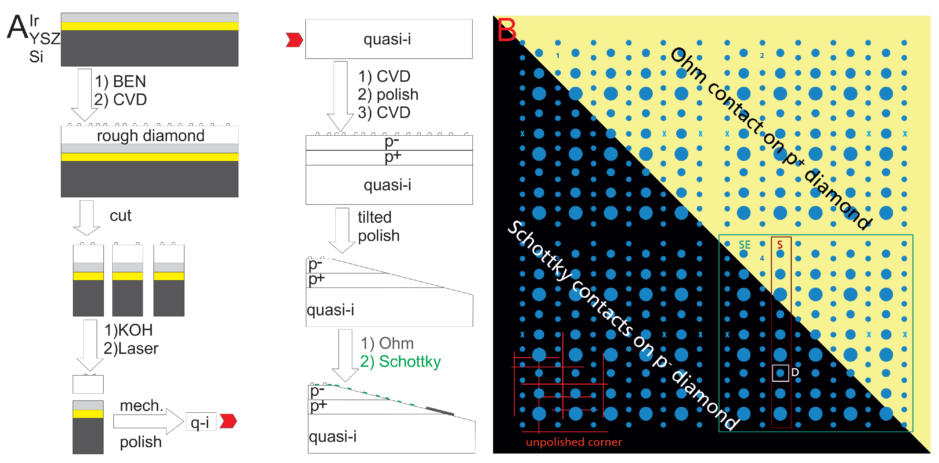
2. Materials and Methods

The fabrication process is illustrated in Figure 1A: Ir/YSZ/Si(001) substrates were made on 2″ Si wafers (N++/As) in an Evatec Clusterline sputtering system. After removing the 2 nm native oxide layer by soft Ar ICP etching (inductively coupled plasma), 45 nm YSZ were grown at 1050 K with a 2:1 Ar/O 2 gas mixture and an RF plasma power of 250 W (4″ Y 0.15 Z r 085 target) following a description by Beshenkov et al. [27]. Then, 120 nm Ir were grown at 975 K with pure Ar and a DC plasma power of 100 W (4″ Ir target) adapting the description by Gsell et al. [23].
Bias-enhanced nucleation (BEN) and initial growth were carried out in a Cornes SDS5200S PECVD reactor with custom adaptations to the sample stage described in previous works [28]. The BEN was performed at 1050 K with a CH 4 /H 2 ratio of 5%, 700 W microwave power and a DC bias of 400 V. The growth into 300 μm thick single-crystalline bulk diamond was performed in an ellipsoid reactor [29] at 1100 K and a microwave plasma power of 12 kW using a CH 4 /H 2 ratio of 1.7%, 1.5‰O 2 and 20 ppm N 2 . The nitrogen acts as growth mediator in the 001 direction, without which, acceptable growth rates cannot be achieved [25].
Afterwards, the resulting rough diamond wafers were lasercut into 9 × 9 mm 2 squares that were separated from the silicon substrate with KOH. The polishing was carried out in two steps: first, a laserpolishing step was performed in which the roughest features were removed by a commercial laser cutting system. Second, mechanical polishing was applied until a smooth surface was reached. Analysis of the crystals by X-ray diffraction shows rocking curve half-widths of the C004 reflex around 0.35°, which involves contributions from both the high-quality topping layer as well as the lower-quality nucleation zone. Concentrations of N and Si are below the detection limit of secondary ion mass spectrometry (SIMS), but photoluminescence analysis shows a P 1 density, i.e., overall nitrogen concentration, of ca. 8 ppm. Silicon vacancy centers were also observed with varying intensities but could not be quantified.
These quasi-intrinsic diamond squares were then overgrown with another short CVD step, which included a 1.5‰B/C doping ratio at 1100 K with 9 kW resulting in p + layers of various thicknesses. After another mechanical polishing step, p layers were deposited at 1100 K with 8 kW. The residual doping of the p- layer stems from the in situ pre-treatment of the p + layers with a H 2 plasma prior to growth, and no further boron was added via the gas phase. After that, a tilted polishing step followed, which allowed for direct access to both p-doped layers. In order to remove hydrogen termination from all areas, which would enable surface conductivity [13], and to create a well-defined oxygen-terminated surface, all samples were treated with nitrating acid.
On the p + region, ohmic Ti/Pt/Au contacts were fabricated by sputtering through a sample-specific handcut shadowmask and subsequently annealing at 1120 K. The Schottky contacts were realized with the identical metal combination with diameters of 100, 150, 200 and 300 μm. They were fabricated via optical laser lithography (Heidelberg Instruments DWL66+), electron beam evaporation and a subsequent lift-off step. In this case, no annealing of the contacts was performed. A schematic end result of this procedure is shown in Figure 1B. For this tilt geometry, the material was barely polished in the bottom left corner, which is why remainders of truncated pyramids are observed there. If the tilt is parallel to the sample edge, there may also be two unpolished corners. For the characterization, diodes will be referred to as “large sector” (SE), “small sector” (S) and the diode number (D) within the corresponding small sector.

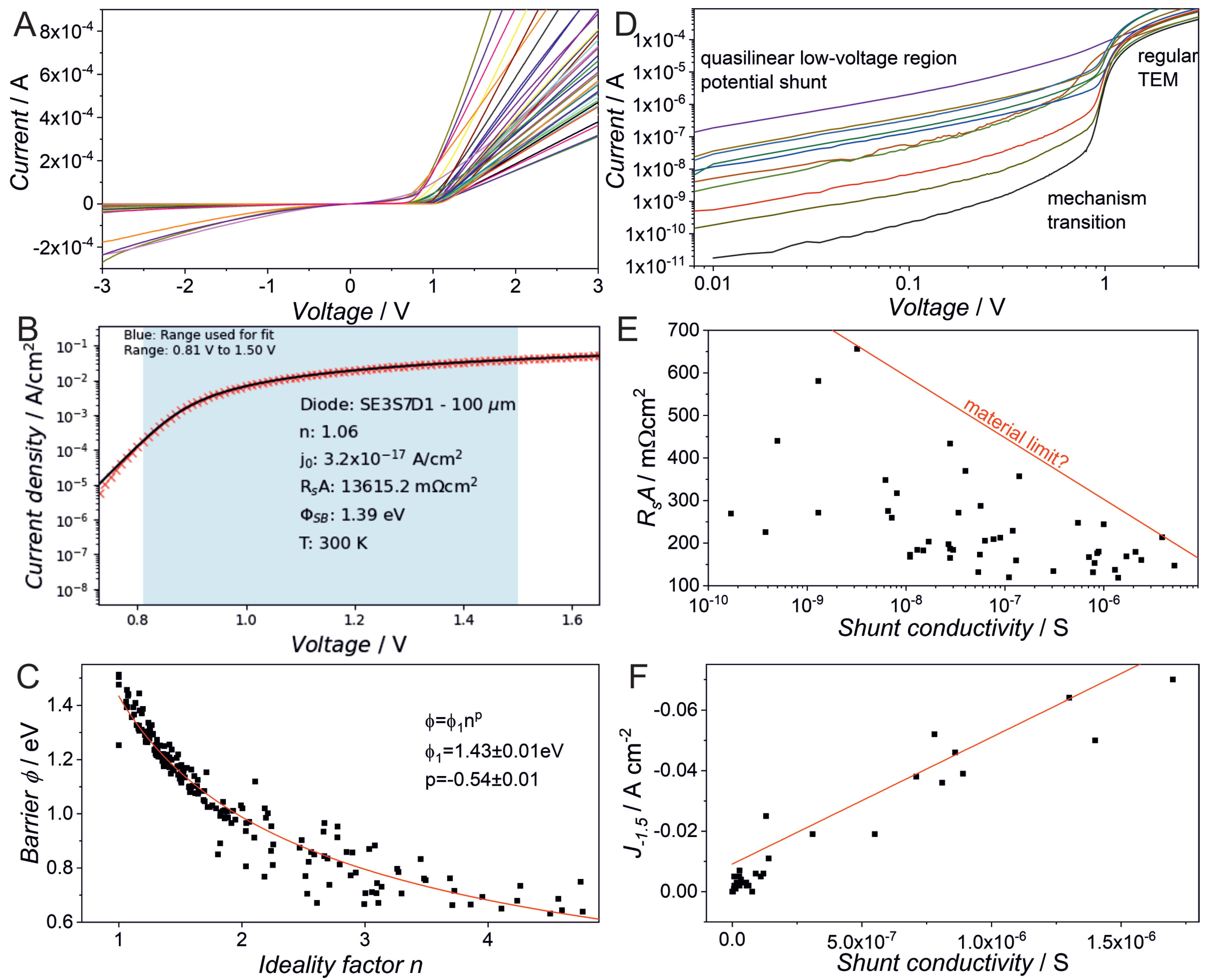
3. Results and Discussion

3.1. Determination of Dopant Concentrations

In order to determine dopant and carrier concentrations, a combination of capacitance–voltage (CV) and SIMS measurements was used. Figure 2A shows the CV profile for one diode from a sample as shown in Figure 1B. From such curves, the profiles of effective acceptor concentrations, N A -N D , were extracted by fitting the second derivative of 1/C 2 with respect to V [30]. Throughout most of this film, the concentration is in the range of 1.2–1.5 × 10 16 cm 3 as demonstrated in Figure 2B. For lower depths, the concentration increases as we come closer to the p + layer.
Boron concentration profiles N B by SIMS for this particular sample are shown in Figure 2C,D. The measurement of the p + layer taken after the growth, but before the intermediate polishing step, shows a plateau at 4.2 × 10 19 cm 3 . A second SIMS measurement taken after the full fabrication in a different location of the same sample also has a plateau corresponding to the p + layer, but, in this case, it is at 5.7 × 10 19 cm 3 . While SIMS has an uncertainty of 10–20%, this is to some extent an actual concentration inhomogeneity caused by locally different growth rates, i.e., by a late coalescence of the initial crystal grains. As the spectrum in panel C was measured on an unpolished surface, it may be speculated that this also contributed to an uncertainty, but since the plateau is on a rather constant height for lower depths, the influence of this may be negligible. Mild differences in the carrier concentrations determined by the CV measurements of the p layers may also be explained by locally differing growth rates in the p + growth since the boron concentration differences from the p + layer may be propagated upwards to some extent. When it comes to the overall thickness, SIMS and CV show a decent enough agreement so that no correction factor has to be applied to CV thicknesses.
Building on the combined CV+SIMS analysis, the three samples that will be discussed have the specifications given in Table 1.

3.2. General Conducting Properties

The current–voltage (I–V) characteristics were investigated for a large set of fabricated diodes. Figure 3A shows the I–V curves for all diodes in one SE of sample II. It is rather apparent that there is a grand variety in the conduction behavior, which, especially due to the variety of the p layer thickness that is discussed later, is no surprise for the forward direction, but, in addition, the reverse direction shows a variation in the leakage currents. On this particular sample, no diode has a leakage current below the detection limit; such diodes were only found on sample I.
The key parameters of the diodes in the forward direction were determined by fitting the current density J in a voltage region selected for each diode individually with the implicit thermionic emission (TEM) current transport model, including series resistance R s [31], which also showed a good agreement for fully vertical diodes on homoepitaxial diamond from our institute [10]:
J T E M = A T 2 e e ϕ S B k B T e e V J R s A n k B T 1
in which, A = 90 Acm 2 K 2 is the Richardson constant for diamond [32], ϕ S B the Schottky barrier, T is the temperature, A is the diode area and n is the ideality factor. k B represents the Boltzmann constant and e represents the elemental charge. The first three voltage-free factors may be gathered into one prefactor j 0 . The lower voltage boundary for which this models yields good agreement varies from diode to diode in the range of 0.7–1.1 V, whereas the upper boundary is less fixed. Figure 3B shows the fit for one of the best rectifying diodes on sample I with an ideality factor of 1.06, a Schottky barrier of 1.39 eV and a series resistance R s A of 13.6 Ωcm 2 .
When the ϕ S B is plotted against n as shown in Figure 3C for all >200 diodes analyzed for this work, a correlation is apparent. The simplest function used to fit this behavior would be of the shape ϕ = ϕ 1 n p , in which, ϕ 1 would be the ideal barrier at n = 1 that, with the test set used here, would be 1.43 eV, which is within the frame found for our Schottky diodes on homoepitaxial diamond [10]. In the homoepitaxial work, the data appeared to be following a linear dependence, whereas the exponent p = −0.54 would be rather close to a 1 / n dependence. If we follow the argumentation by R. Tung [33] (see subsections 5.3 and 9.3 therein), the existence of ideality factors 1 and a dependence of ϕ S B on n indicates that the Schottky barrier itself is, to some extent, voltage-dependent. Tung’s argumentation was derived assuming a combination of image-force barrier lowering and carrier tunneling; in our case, either the underlying physics or at least the barrier shape changes would have to be attributed to a different effect.
At lower voltages, the curve shows significant deviations from the TEM model. A double logarithmic plot as shown in Figure 3D exhibits a mechanism transition just below 1 V forward voltage. The shape is almost linear since the fitting of the double logarithmic graphs yields slopes in the range of 1.1–1.2. Such a behavior indicates the existence of shunt conductance [34,35]. In the case of our homoepitaxial diodes [10], this had been considered an option, but the low-voltage behavior there had exhibited a better match with a second-barrier mechanism, which, in this case, seemed less fitting.
Relations between the shunt conductivity and other material parameters can be observed. While the series resistance R s A has no functional correlation to the shunt conductivity as depicted in Figure 3E, there seems to be some sort of material limit line. This indicates two things: first, the shunt conduction, in principle, occurs via different channels to the conduction at higher voltages, which is dominated by the bulk of the p layer; second, when the shunt conduction channels become powerful enough to cross a certain limit, they prevent the series resistance from developing the potential value, which it would have for a close-to-ideal crystal. While the shunt conductivity has no functional correlation to R s A , there is a clear linear relation to the leakage currents as illustrated by Figure 3F. Therefore, both shunt and leakage conduction probably go through the same channels; a more thorough discussions of the leakage phenomena follows below.
The serial resistance R s A shows a great variety ranging from 0.03 to 25 Ωcm 2 , but no correlation to any of the other fitting parameters can be found. However, it shows an expectable dependence on the film thickness as shown by Figure 4A,B: in the regions in which the p layer was partially polished off, it is lower than in the regions in which it remained essentially untouched. A plot of current densities at a random forward voltage would logically exhibit the diametrical behavior.
A mapping of leakage currents at −1.5 V reverse voltage as shown in Figure 4C shows no fully systematic behavior with respect to the position. While there are some highly leaky diodes directly at the p /p + border, there is no systematic decay towards the thicker p layer, but there are randomly distributed local maxima in all areas of the sample. For the larger diameters, the occurence of highly leaky behavior seems to be more abundant. This indicates that the leakage current is not determined by the thickness or a potential surface conductivity by eventual incomplete hydrogen removal, but rather by local defects. It has to be stated that the incompletely polished regions in the sample corners must not be considered as defected in this regard since no outstanding leakage phenomena were observed in these areas.
Therefore, we looked deeper into the leakage phenomena. Figure 5A displays the leakage current density for two formally similar diodes, which shows a substantially higher J for the upper diode SE1S3D7, which is formally further away from the p + region. The obvious reason for this can be found in the micrograph: this diode is located over the boundary of a penetration twin. These entities often occur in the growth of heteroepitaxial diamond as we have discussed in previous works [25,36]. Their incoherent boundary is a good channel for leakage current to go through. Such twins were also reported in the work by Sittimart et al. [22], leading to similar issues. It is obvious that the growth requires further optimization in order to get rid of these channels.
In our previous work [25] we also discussed the appearance of other defects, such as (111) stacking faults or edge-type 1/2[100]|(100) threading dislocations. Particularly for the latter, it is often speculated that they may locally harbor sp 2 hybridized carbon moieties, which would be a good candidate for promoting enhanced vertical electrical transport, causing a higher level of the leakage current.
We also checked the conduction mechanism of the leakage: as Figure 5B shows, there is a transition. The slope in the double logarithmic plot is ca. 1 for low voltages and transitions to values of around 2 at a certain point. Such behavior is typical for space-charge limited conduction [37,38]. We also checked at higher voltages whether a transition to a trap-filled behavior occurs, which would have a characteristic temperature dependence, but we did not observe that.
Finally, for sample I, which is the only one that has diodes without any detectable leakage current at low voltages, breakdown measurements were performed. For the longest-lasting diodes, a breakdown curve as shown in Figure 5C was obtained. Since there is no hard breakdown, a well-defined breakdown voltage is hard to assign, but the increase at 105 V, which also marks the crossing of the 1 A/cm 2 mark, can be seen as a reasonable assignment for the breakdown voltage V B D of this particular diode. If this diode would actually be operated, 60 V would probably be the maximum recommendable voltage. At the location of this particular diode, the p layer is ca. 0.7 μm thick, which yields a breakdown field of 1.5 MV/cm, which would be similar to the value reported by Kwak et al. [21]. With these measurements, it is also possible to calculate a Baliga Figure of Merit [39] BFOM = V B D 2 /( R s A ) of 810 W/cm 2 , which, of course, is still much below any value of recent works for homoepitaxy. In addition, at the moment, such a behavior is only observed for the best analyzed diodes, while many already exhibit significant leakage between 20 and 50 V.
Therefore, it is an obvious objective to reach a decent breakdown field for the majority of diodes instead of the current fraction. It would also be desirable to increase the layer thickness in order to reach higher absolute breakdown voltages. Since our growth parameters involve a fast growth in the 111 direction, pre-existing penetration twins with a topping 111 facet will outgrow the rest of the material very fast. In order to move to more advanced devices, eliminating these twins at an earlier growth stage is also a requirement.

4. Conclusions and Outlook

We have demonstrated the fabrication of pseudovertical Schottky barrier diodes based on heteroepitaxially grown diamond substrates. In-depth characterization were undertaken with respect to diode characteristics, such as rectification and breakdown voltage, which, for the best diodes, reached suitable values. Shunt conductance in the forward direction and associated leakage in the reverse direction could be related to crystal defects such as twins and boundaries.
While the first functional devices have been successfully implemented, future efforts are needed for the improvement of the underlying material properties. Besides the reduction in impurities and defects, novel processes will be implemented. A scalable technology could proceed via etching for contacting the p + layers instead of the tilted polishing step. Once that is achieved, targeting more sophisticated devices will be enabled in the future.

Author Contributions

Ir template preparation: J.W.; diamond nucleation and growth: J.K., J.E., V.L. and P.R.; SIMS and XRD: P.S. and L.K.; diode fabrication: F.B. and C.G.; diode characterization: J.W., P.R. and H.C.; Python script for implicit fitting of the TEM model: P.R. All authors have read and agreed to the published version of the manuscript.

Funding

The development of the diamond fabrication process was funded by the Wehrtechnische Dienststelle für Informationstechnologie und Elektronik (WTD 81) of the Federal Ministry of Defence (BMVG). The diode fabrication was funded by the board project QuaComVor of the Fraunhofer Society.

Informed Consent Statement

Not applicable.

Data Availability Statement

Source data are available from the authors upon reasonable request.

Acknowledgments

The authors thank Silas Pokorny, Mario Prescher, Michael Ardner and Matthias Sinnwell for practical support.

Conflicts of Interest

The authors declare no conflict of interest.

Abbreviations

BDDBoron-Doped Diamond
BENBias Enhanced Nucleation
BFOMBaliga Figure of Merit
CVCapacitance–Voltage
CVDChemical Vapor Deposition
HPHTHigh-Pressure–High-Temperature
MDPIMultidisciplinary Digital Publishing Institute
MPCVDMicrowave Plasma CVD
SIMSSecondary Ion Mass Spectrometry
TEMThermionic Emission

References

  1. Araujo, D.; Suzuki, M.; Lloret, F.; Alba, G.; Villar, P. Diamond for electronics: Materials, processing and devices. Materials 2021, 14, 7081. [Google Scholar] [CrossRef]
  2. Donato, N.; Rouger, N.; Pernot, J.; Longobardi, G.C.; Udrea, F. Diamond power devices: State of the art, modelling, figures of merit and future perspective. J. Phys. D. Appl. Phys. 2020, 53, 093001. [Google Scholar] [CrossRef] [Green Version]
  3. Perez, G.; Maréchal, A.; Chicot, G.; Lefranc, P.; Jeannin, P.O.; Eon, D.; Rouger, N.; Perez, G.; Maréchal, A.; Chicot, G.; et al. Diamond semiconductor performances in power electronics applications. Diam. Relat. Mater. 2020, 110, 108154. [Google Scholar] [CrossRef]
  4. Shikata, S. Single crystal diamond wafers for high power electronics. Diam. Relat. Mater. 2016, 65, 168–175. [Google Scholar] [CrossRef] [Green Version]
  5. Gerrer, T.; Czap, H.; Maier, T.; Benkhelifa, F.; Müller, S.; Nebel, C.E.; Waltereit, P.; Quay, R.; Cimalla, V. 3 GHz RF measurements of AlGaN/GaN transistors transferred from silicon substrates onto single crystalline diamond. AIP Adv. 2019, 9, 125106. [Google Scholar] [CrossRef] [Green Version]
  6. Tarelkin, S.; Bormashov, V.; Buga, S.G.; Volkov, A.; Teteruk, D.; Kornilov, N.; Kuznetsov, M.; Terentiev, S.; Golovanov, A.; Blank, V. Power diamond vertical Schottky barrier diode with 10 A forward current. Phys. Status Solidi A 2015, 212, 2621–2627. [Google Scholar] [CrossRef]
  7. Zhao, D.; Liu, Z.; Wang, J.; Yi, W.; Wang, R.; Wang, K.; Wang, H. Performance Improved Vertical Diamond Schottky Barrier Diode with Fluorination-Termination Structure. IEEE Electron Device Lett. 2019, 40, 1229–1232. [Google Scholar] [CrossRef]
  8. Murooka, T.; Yaita, J.; Makino, T.; Ogura, M.; Kato, H.; Yamasaki, S.; Natal, M.; Saddow, S.E.; Iwasaki, T.; Hatano, M. Characterization of Schottky Barrier Diodes on Heteroepitaxial Diamond on 3C-SiC/Si Substrates. IEEE Trans. Electron Devices 2020, 67, 212–216. [Google Scholar] [CrossRef]
  9. Arnault, J.C.; Lee, K.; Delchevalrie, J.; Penuelas, J.; Mehmel, L.; Brinza, O.; Temgoua, S.; Stenger, I.; Letellier, J.; Saint-girons, G.; et al. Epitaxial diamond on Ir / SrTiO 3 / Si(001): From sequential material characterizations to fabrication of lateral Schottky diodes. Diam. Relat. Mater. 2020, 105, 107768. [Google Scholar] [CrossRef]
  10. Reinke, P.; Benkhelifa, F.; Kirste, L.; Czap, H.; Pinti, L.; Zurbig, V.; Cimalla, V.; Nebel, C.; Ambacher, O. Influence of Different Surface Morphologies on the Performance of High-Voltage, Low-Resistance Diamond Schottky Diodes. IEEE Trans. Electron Devices 2020, 67, 2471–2477. [Google Scholar] [CrossRef]
  11. Kawarada, H.; Yamada, T.; Xu, D.; Tsuboi, H.; Saito, T.; Hiraiwa, A. Wide temperature (10K-700K) and high voltage (1000V) operation of C-H diamond MOSFETs for power electronics application. In Proceedings of the 2014 IEEE International Electron Devices Meeting, San Francisco, CA, USA, 15–17 December 2014; pp. 11.2.1–11.2.4. [Google Scholar] [CrossRef]
  12. Masante, C.; Rouger, N.; Pernot, J. Recent progress in deep-depletion diamond metal – oxide – semiconductor field-effect transistors. J. Phys. D. Appl. Phys. 2021, 54, 233002. [Google Scholar] [CrossRef]
  13. Alhasani, R.; Yabe, T.; Iyama, Y.; Oi, N.; Imanishi, S.; Nguyen, Q.N.; Kawarada, H. An enhanced two-dimensional hole gas (2DHG) C–H diamond with positive surface charge model for advanced normally-off MOSFET devices. Sci. Rep. 2022, 12, 4203. [Google Scholar] [CrossRef] [PubMed]
  14. Hatano, M.; Iwasaki, T.; Yamasaki, S.; Makino, T. Diamond electronics. In Proceedings of the 46th European Solid-State Device Research Conference, Lausanne, Switzerland, 2–15 September 2016; pp. 330–332. [Google Scholar] [CrossRef]
  15. Iwasaki, T.; Hoshino, Y.; Tsuzuki, K.; Kato, H.; Makino, T.; Ogura, M.; Takeuchi, D.; Matsumoto, T.; Okushi, H.; Yamasaki, S.; et al. Diamond junction field-effect transistors with selectively grown n+-side gates. Appl. Phys. Express 2012, 5, 091301. [Google Scholar] [CrossRef]
  16. Takeuchi, D.; Koizumi, S.; Makino, T.; Kato, H.; Ogura, M.; Ohashi, H.; Okushi, H.; Yamasaki, S. Negative electron affinity of diamond and its application to high voltage vacuum power switches. Phys. Status Solidi A 2013, 210, 1961–1975. [Google Scholar] [CrossRef]
  17. Zhu, X.; Liu, J.; Shao, S.; Tu, J.; Huang, Y.; Bi, T.; Chen, L.; Wei, J.; Kawarada, H.; Li, C. Evolution of growth characteristics around the junction in the mosaic diamond. Diam. Relat. Mater. 2021, 120, 108640. [Google Scholar] [CrossRef]
  18. Ando, Y.; Sawabe, A. Heteroepitaxy of Diamond. In Physics and Applications of CVD Diamond; Koizumi, S., Nebel, C.E., Nesladek, M., Eds.; Wiley-VCH: Berlin, Germany, 2008; Chapter 4; pp. 77–92. [Google Scholar] [CrossRef]
  19. Schreck, M.; Gsell, S.; Brescia, R.; Fischer, M. Ion bombardment induced buried lateral growth: The key mechanism for the synthesis of single crystal diamond wafers. Sci. Rep. 2017, 7, 44462. [Google Scholar] [CrossRef] [PubMed] [Green Version]
  20. Kawashima, H.; Noguchi, H.; Matsumoto, T.; Kato, H.; Ogura, M.; Makino, T.; Shirai, S.; Takeuchi, D.; Yamasaki, S. Electronic properties of diamond Schottky barrier diodes fabricated on silicon-based heteroepitaxially grown diamond substrates. Appl. Phys. Express 2015, 8, 104103. [Google Scholar] [CrossRef]
  21. Kwak, T.; Lee, J.; Choi, U.; So, B.; Yoo, G.; Kim, S.; Nam, O. Diamond Schottky barrier diodes fabricated on sapphire-based freestanding heteroepitaxial diamond substrate. Diam. Relat. Mater. 2021, 114, 108335. [Google Scholar] [CrossRef]
  22. Sittimart, P.; Ohmagari, S.; Yoshitake, T. Enhanced in-plane uniformity and breakdown strength of diamond Schottky barrier diodes fabricated on heteroepitaxial substrates. Jpn. J. Appl. Phys. 2021, 60. [Google Scholar] [CrossRef]
  23. Gsell, S.; Bauer, T.; Goldfuß, J.; Schreck, M.; Stritzker, B. A route to diamond wafers by epitaxial deposition on silicon via iridium/yttria-stabilized zirconia buffer layers. Appl. Phys. Lett. 2004, 84, 4541–4543. [Google Scholar] [CrossRef]
  24. Yoshikawa, T.; Kodama, H.; Kono, S.; Suzuki, K.; Sawabe, A. Wafer bowing control of free-standing heteroepitaxial diamond (100) films grown on Ir(100) substrates via patterned nucleation growth. Thin Solid Films 2015, 594A, 120–128. [Google Scholar] [CrossRef]
  25. Lebedev, V.; Engels, J.; Kustermann, J.; Weippert, J.; Cimalla, V.; Kirste, L.; Giese, C.; Quellmalz, P.; Graff, A.; Meyer, F.; et al. Growth Defects in Heteroepitaxial Diamond. J. Appl. Phys. 2021, 129, 165301. [Google Scholar] [CrossRef]
  26. Schreck, M.; Mayr, M.; Klein, O.; Fischer, M.; Gsell, S.; Sartori, A.F.; Gallheber, B.C. Multiple role of dislocations in the heteroepitaxial growth of diamond: A brief review. Phys. Status Solidi A 2016, 213, 2028–2035. [Google Scholar] [CrossRef]
  27. Beshenkov, V.G.; Znamenskii, A.G.; Marchenko, V.A.; Pustovit, A.N.; Chernykh, A.V. Extension of the temperature range of epitaxial YSZ film growth on Si(100) during magnetron sputtering. Tech. Phys. 2007, 52, 636–641. [Google Scholar] [CrossRef]
  28. Yoshikawa, T.; Herrling, D.; Meyer, F.; Burmeister, F.; Nebel, C.E.; Ambacher, O.; Lebedev, V. Influence of substrate holder configurations on bias enhanced nucleation area for diamond heteroepitaxy: Toward wafer-scale single-crystalline diamond synthesis. J. Vac. Sci. Technol. B 2019, 37, 021207. [Google Scholar] [CrossRef]
  29. Füner, M.; Wild, C.; Koidl, P. Novel microwave plasma reactor for diamond synthesis. Appl. Phys. Lett. 1998, 72, 1149–1151. [Google Scholar] [CrossRef]
  30. Rhoderick, E.H.; Williams, R.H. The capacitance of a Schottky Barrier. In Met. Contacts, 2nd ed.; Hammond, P., Grimsdale, R., Eds.; Oxford University Press: New York City, NY, USA, 1988; pp. 141–181. [Google Scholar]
  31. Cordes, L.F.; Garfinkel, M. High voltage power Schottky diodes. In Proceedings of the IEEE Power Electronics Specialists Conference, Murray Hill, NJ, USA, 10–12 June 1974; IEEE: Murray Hill, NJ, USA, 1974; pp. 205–213. [Google Scholar] [CrossRef]
  32. Blank, V.D.; Bormashov, V.S.; Tarelkin, S.A.; Buga, S.G.; Kuznetsov, M.S.; Teteruk, D.V.; Kornilov, N.V.; Terentiev, S.A.; Volkov, A.P. Power high-voltage and fast response Schottky barrier diamond diodes. Diam. Relat. Mater. 2015, 57, 32–36. [Google Scholar] [CrossRef]
  33. Tung, R.T. Recent advances in Schottky barrier concepts. Mater. Sci. Eng. R 2001, 35, 1–138. [Google Scholar] [CrossRef]
  34. Banwell, T.C.; Jayakumar, A. Exact analytical solution for current flow through diode with series resistance. Electron. Lett. 2000, 36, 291–292. [Google Scholar] [CrossRef]
  35. Jung, W.; Guziewicz, M. Schottky diode parameters extraction using Lambert W function. Mater. Sci. Eng. B Solid-State Mater. Adv. Technol. 2009, 165, 57–59. [Google Scholar] [CrossRef]
  36. Lebedev, V.; Yoshikawa, T.; Giese, C.; Kirste, L.; Žukauskaite, A.; Graff, A.; Meyer, F.; Burmeister, F.; Ambacher, O. Formation of icosahedron twins during initial stages of heteroepitaxial diamond nucleation and growth. J. Appl. Phys. 2019, 125, 075305. [Google Scholar] [CrossRef]
  37. Chiu, F.C. A Review on Conduction Mechanisms in Dielectric Films. Adv. Mater. Sci. Eng. 2014, 2014, 578168. [Google Scholar] [CrossRef] [Green Version]
  38. Child, C.D. Discharge from hot platinum wires. Phys. Rev. Ser. I 1911, 32, 492–511. [Google Scholar] [CrossRef]
  39. Baliga, B.J. Power Semiconductor Device Figure of Merit for High-Frequency Applications. IEEE Electron Device Lett. 1989, 10, 455–457. [Google Scholar] [CrossRef]
Figure 1. (A): Illustration of the growth process: Dia/Ir/YSZ/Si(001) was grown by BEN and CVD; the resulting substrate was cut into square-shaped pieces and the diamond was separated from the rest of the material. After mechanical polishing, the resulting quasi-intrinsic substrate was overgrown with a p + layer, polished again and overgrown again with a p layer. A tilted mechanical polish allows for access to all layers. The ohmic contact was deposited on the p + region, whereas the smaller contacts for Schottky diodes were distributed over the whole substrate. (B): Schematic representation of a finished sample. For the characterizations in the further sections, the diodes were indexed by large sectors (SE), small sectors (S) and diode indices (D) within the sectors. The Ohmic contact extends over almost the entire p + zone.
Crystals 12 01626 g001
Figure 2. (A): CV measurement for diode SE1S3D11 on a sample (denoted I in Table 1 below) prepared as shown in Figure 1A; (B): carrier concentration determined from fitting the second derivative of the CV measurement; (C): SIMS after the growth of the p + layer before polishing; (D): SIMS at the final stage in one of the least polished locations.
Crystals 12 01626 g002
Figure 3. (A): Current–voltage plot for all characterized diodes in SE4 on sample II. If not specified otherwise, a positive voltage will be the forward direction and a negative voltage the reverse direction for all following data; (B): TEM model fit for diode SE3S7D1 on sample I; (C): correlation of the Schottky barrier ϕ S B and the ideality factor n for all investigated diodes on all samples; (D): double logarithmic plot for the low-voltage region for a set of diodes on sample II exhibiting an almost linear behavior; (E): plot of R s A vs. the shunt resistance for all 100 μm diodes on the same sample; (F): plot of the leakage current density at −1.5 V J 1.5 for the same diodes exhibiting a linear correlation between low-voltage forward and reverse conduction.
Crystals 12 01626 g003
Figure 4. (A): Interference contrast micrograph of SE1 + SE2 sample III. The red line roughly marks the border at which the p + and p regions are exposed after the polishing. The x markers correspond to the markers in panel C. (B): Mapping of R s A for all diodes measured on this sample with a clear thickness dependence; the arrangement on the chart exactly matches the arrangement of the diodes above. (C): Mapping of leakage current densities at −1.5 V reverse voltage showing no systematic regional dependencies.
Crystals 12 01626 g004
Figure 5. (A): Comparison of two diodes from sample III, where the upper diode on the penetration twin has a much stronger leakage current despite being further away from the p + region; (B): temperature-dependent leakage current density measurements of one of the diodes on sample II with a low-voltage ohmic regime and a space-charge regime at higher voltages; (C): breakdown measurement for the diode on sample I from Figure 3B.
Crystals 12 01626 g005
Table 1. Key parameters of the three samples referenced in this work.
Sample IDN B , p + (cm 3 )N A -N D , p (cm 3 )
I5 × 10 19 1.4 × 10 16
II7 × 10 19 8 × 10 15
III1 × 10 20 5 × 10 14
Publisher’s Note: MDPI stays neutral with regard to jurisdictional claims in published maps and institutional affiliations.

