Review

A Review on Ultrafast-Laser Power Bed Fusion Technology

Defense Innovation Institute, Academy of Military Science, Beijing 100072, China
*
Author to whom correspondence should be addressed.
Crystals 2022, 12(10), 1480; https://doi.org/10.3390/cryst12101480
Submission received: 26 September 2022 / Revised: 14 October 2022 / Accepted: 17 October 2022 / Published: 18 October 2022

Abstract

:
Additive manufacturing of metals by employing continuous wave and short pulse lasers completely changes the way of modern industrial production. But the ultrafast laser has the superiority to short pulse laser and continuous wave laser in additive manufacturing. It has higher peak power, small thermal effect, high machining accuracy and low damage threshold. It can effectively perform additive manufacturing for special materials and improve the mechanical properties of parts. This article reviews the mechanism of the interaction between ultrafast laser and metal materials to rule the manufacturing processes. The current application of ultrafast laser on forming and manufacturing special materials, including refractory metals, transparent materials, composite materials and high thermal conductivity materials are also discussed. Among the review, the shortcomings and challenges of the current experimental methods are discussed as well. Finally, suggestions are provided for the industrial application of ultrashort pulse laser in the field of additive manufacturing in the future.

1. Introduction

In the past few decades, additive manufacturing (AM) technology has received widespread attention due to its ability to create three-dimensional free structures of almost any geometric shape. Selective laser melting (SLM, also termed Laser Powder Bed Fusion) is one of the most common and attractive AM technologies that directly forms three-dimensional complex components according to a digital model by adding material layer by layer [1]. Although continuous wave (CW) laser and short pulse laser have been widely used in the field of laser machining, there are still some limitations and disadvantages. For example: some special materials with high melting point or high reflectivity continue to pose challenges and are difficult to process [2]; some micro engines must be manufactured with remarkable precision at the micro level [3]. A more effective method to reach very high temperatures while causing minimal heat affected zone (HAZ) is needed to process such materials.
With the development of laser technology, researchers can use mode locking to generate pulses of femtosecond (fs) or picosecond (ps) duration with higher peak intensities compared to CW lasers or long-pulsed lasers. For the extension of the application field of the femtosecond laser processing, several efforts including various theoretical and experimental studies have already been made so far. It has been demonstrated that as the pulse width decreases from nanosecond to femtosecond, the heat affected area of the metal solids is suppressed and the processing quality can be significantly improved [4,5,6]. During ultrafast pulse laser interaction with materials, laser allow for rapid energy delivery into the material (~ps), which is significantly faster than plasma expansion time (from ns to µs). Heat accumulation combined with high peak powers of ultrafast pulse laser increases the local temperature rapidly rise to temperatures as high as 6000 °C, while the surrounding area is still cold. Benefiting from ultrashort pulse width and smaller energy input to the materials, the usage of ultrafast laser in high quality manufacturing processes can reduce heat dissipation and thus reduce HAZ in the surrounding environment. This highly intensively pulse with a duration of less than picoseconds can modify or ablate materials, creating precise features on micro- and nano-scales in a highly localized and controlled manner [7]. Thus the use of ultrafast pulse lasers as a manufacturing tool is gaining significant momentum across industries [8,9]. Though the applications of ultrafast lasers in laser AM have not been extensively studied yet, they have been widely used for various material processing such as drilling, micro-structuring and glass welding [10,11,12,13,14] with its unique characteristics of ultrashort pulse width and extremely high peak intensity. Compared with CW laser and short pulse laser, ultrafast pulse laser can increase part resolution, possess rapid cooling rate, minish residual stresses, reduce oxidation effect and decrease substrate damage [7]. In this regard, ultrafast lasers are well suited for lifting the shortcomings of the existing laser AM techniques, especially in situations where high melting point materials are involved or extreme precision and reproducibility are required.
While femtosecond laser-based AM is still in its infancy, this review is an attempt to highlight some of the fs laser-based research endeavors, identify the intended applications and outline prospects of the fs laser AM. We summarize the research status of ultrashort pulse laser manufacturing. Namely this article discusses the process of the interaction between ultrashort pulse laser and materials, and reviews current research status of ultrashort pulse laser SLM process in four special processing fields: refractory metals, transparent material, multi-material layered structure and high thermal conductivity materials. Among these, the influence of laser power, scan rate and other process parameters on the forming quality of the parts are analyzed, and the research hotspots and existing problems in the current ultrashort pulse laser forming manufacturing process are also put forward, aiming to provide a practical and effective reference for the research of SLM process.

2. Theoretical Research on the Interaction between Ultrashort Pulse Laser and Solid Materials

In SLM, melting takes place due to the absorption of the thermal energy resulting from the laser–matter interaction. Consider specific heat capacity and latent heat vary from one material to another, inappropriate laser parameters may affect the final product’s quality. From the theoretical point of view the ultrashort time of excitation allows the separation of the involved processes as excitation, melting, and material removal. Compared with continuous laser and short pulse laser, ultrashort pulse laser have two notable characteristics: (1) extremely short pulse time, even on the femtosecond scale; (2) generating extremely high levels of 1013–1014 W/cm2 energy density. In some cases, the provision of insufficient energy affects the material build quality, leading to detrimental structural impacts. Extremely high laser power can result in excessive evaporation of molten material, even generates deep grooves in the center of the wall [15]. While ultrafast lasers are distinguished mainly by three factors: extremely short pulse duration, high intensity and a broad spectral bandwidth [16]. Through theoretical studies, researchers can explain the advantages of ultrafast lasers, guide process parameters and provide guidance for future research.

2.1. Mechanisms of Ultrafast Laser–Matter Interaction

In a single laser–materials interactions, fs lasers allow for rapid energy delivery into the material (~ps) [17], the whole process of heat transfer between ultrafast laser and solid material can be divided into two steps [18]. The first step starts with the deposition of laser energy into the material, including the spatial and temporal distribution of energy. The second step is the process in which the energy deposited in the material is conducted inside the material through free electrons or lattice vibrations after irritation. Since most metals are opaque to visible light, the laser energy is deposited in the penetration depth range at the beginning of the process and then gradually transferred to the thermal diffusion depth under conventional heat transfer equations.
The interaction mechanism between the femtosecond laser and the material can be obtained as shown in Figure 1 [19]. It can be found that the pulse width of the ultrashort pulse laser is less than the electron-grain relaxation time (10–100 ps), so when the ultrashort pulse laser interacts with the material, only the free electrons on the top of the material can absorb the energy of the ultrashort pulse laser electrons in the conduction band absorb photons and gain higher energy. At this time, the electrons are heated to a high temperature as shown in Figure 1a, this excitation of the solid takes place during the laser pulse, and the lattice system is still at an ambient temperature as shown in Figure 1b. Due to the interaction of laser and matter, only the process of electrons being stimulated to absorb and storing energy occurs, which fundamentally avoids the transfer and conversion of energy, as well as the existence and thermal diffusion of thermal energy [20]. Therefore, the heat transfer mechanism between the ultrashort pulse laser and the material is different from the traditional heat transfer theory (Fourier law). After the laser pulse depositing energy, the nonequilibrium of temperatures drives the energy exchange between electrons and phonons. Thus, the thermodynamic equilibrium between the electronic system and the crystal lattice can be reached after multiple electron-phonon relaxation times (in the range of picoseconds) as shown in Figure 1c. Since the electron–phonon coupling strength depends on the properties of the conduction band electrons, the characteristic relaxation time of the temperature equilibration leads to a huge difference between different materials. Through this thermal conduction mechanism, the strength of the electron-phonon coupling determines the energy loss of the ultrashort pulse laser into the material and thermal damage zone [21]. The literature [22] pointed out that the electron-phonon coupling coefficient of the material has a decisive effect on the energy transfer. Corkum [23] also pointed out that the heat transfer range is determined by the electro-phonon coupling coefficient. So, the physical properties of the material and parameters such as the pulse time of the laser will significantly affect the energy absorption of the powder and the shape of the molten pool, and ultimately affect the performance of the products [24].
Extremely narrow pulse duration of femtosecond lasers allows extremely small energies to reach extremely high powers compared to CW or short pulse laser. Since most of the electron energy transferers to the crystal lattice through the electron-phonon coupling process, with almost no thermal diffusion, so that the thermal damage of the metal is limited to a small laser focus area [25,26]. While the CW and short pulse laser is different. The electron energy diffuses in the metal for a longer time, resulting in lower precision of CW and short pulse laser processing and higher HAZ.
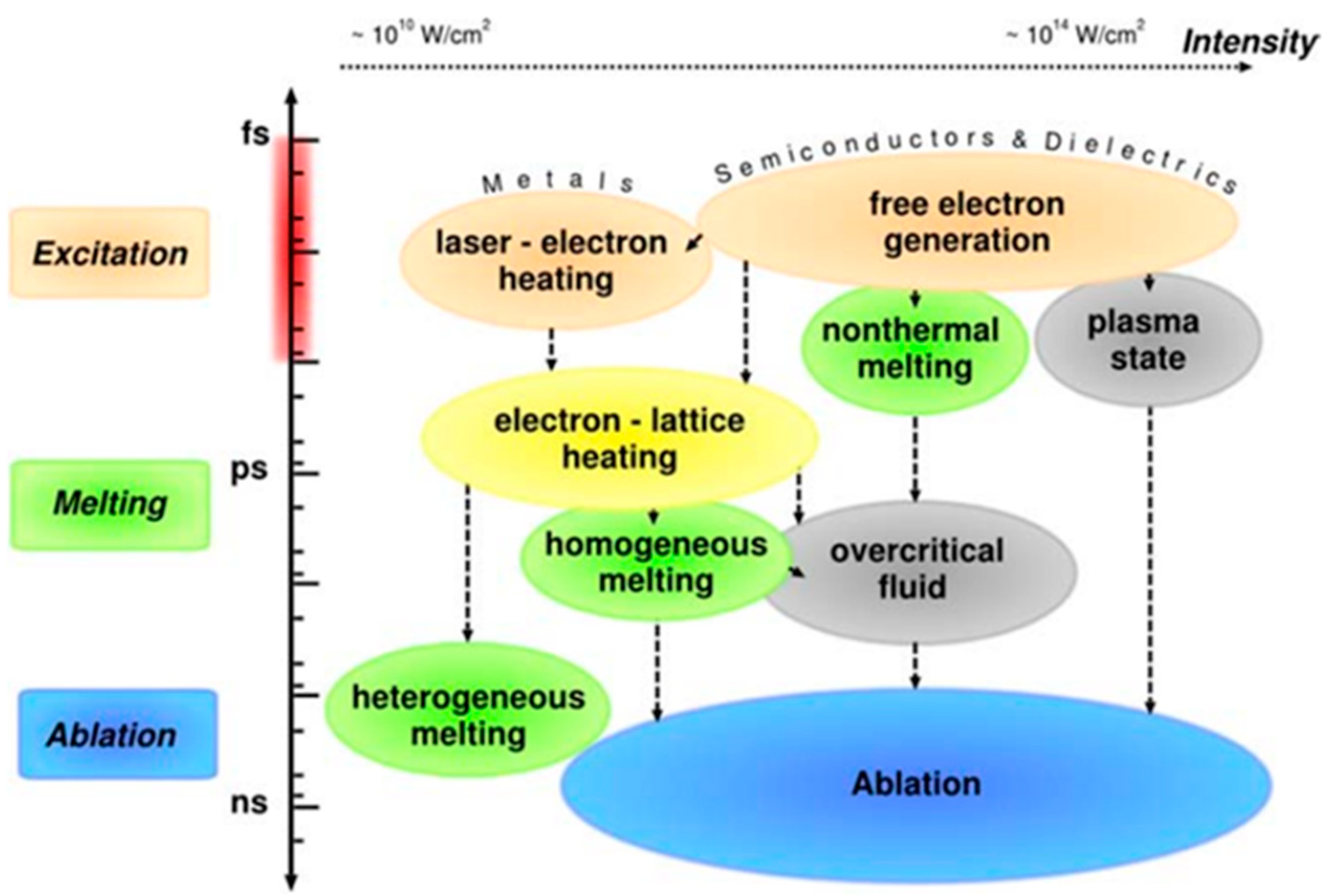
Based on different material and laser parameters, a series of phenomena which shows a very strong threshold effect begin to occur after laser irritation. An overview of typical involved phenomena in the considered parameter range is given in Figure 2 which shows pathways of the material from excitation to ablation, depending on the relevant timescale and intensity ranges [27]. When the laser energy exceeds the melting threshold, the material surface exhibits heterogeneous melting and gradually stabilizes; while exceed ablation threshold, the relaxation after homogeneous melting of the surface results in the expansion of the surface, followed by the generation of tensile stress waves, and when the tensile stress is large enough the matter is going to move, which is also called spallation; laser energy further reaches the evaporation threshold, the material will evaporate and even become plasma, the phase explosion state is reached. Thus, selecting a suitable processing parameters window based on the mechanism of action is necessary, it can also be used to microscopically analyze the non-equilibrium phase transition process of the interaction between ultrashort pulse laser and metal.

2.2. Numercial Simulation of Ultrafast Laser–Matter Interaction

The process of interaction between the ultrafast laser and materials is very complex, the time and space involved are very wide and the existing monitoring methods are almost impossible to visually characterize these microscopic phenomena during the printing process. As a result, it is a reliable solution to study the interaction details by numerical models and provide parameter windows for experiments. With the deepening of research on the interaction between laser and solid materials, the theory of interaction between ultrashort pulse laser and solid materials has been further developed. Among them, some new theoretical models have been proposed, such as two temperature model(TTM) [28], molecular dynamics model(MD) [29], fluid Dynamics Model (FD) [30] and so on. The TTM is used to describe the process of fs laser-matter interaction: when a metal is irradiated by an ultrashort pulse laser, its electrons and photons absorb the laser energy within the ultrashort pulse duration, and then electron-phonon interactions assign energy to the lattice, which is described as:
{ C e T e t = x ( κ e ( T e , T l ) T e x ) G ( T e T l ) + I ( z , t ) C l T l t = x ( κ l ( T l ) T l x ) + G ( T e T l )
where C is the heat capacity, κ is the thermal conductivity and G is the electron-phonon coupling factor, and their subscripts e and l are electron and lattice, and I ( z , t ) is the laser heating source term. TTM can well describe the process of electron absorption of laser energy, energy transfer between electrons and phonons, etc., but TTM cannot be used to observe the deformation of ultrashort pulse laser radiation targets. MD simulation can calculate the motion trajectories and interactions of atoms and molecules. It is an effective tool to analyze the thermodynamic behavior of femtosecond laser ablation of metal materials from a microscopic perspective. MD can simulate the processes including melting, ablation, spalling and microstructural evolution of metals under ultrashort pulsed laser radiation. The FD can be used to simulate dynamic processes such as phase transitions and metastable states during the interaction between femtosecond lasers and metals based on the conservation of mass, momentum and energy. But the FD methods oversimplify the process of laser absorption. In addition, FD at the microscale is computationally challenging, as it requires considering micro time steps, which increases the computational costs. These three models have their own advantages and disadvantages, and they are generally used in combination with each other. They allow for realizing a better understanding underlying physical interactions of the processes and their effects on the quality of the manufactured part.
When the laser energy is below the threshold, it is not enough to melt the powder. Above this threshold, a homogeneous melting track could be generated. A further increase of the pulse energy would result in the blasting effect at the center of the track, where the particles in the focus were ablated/blasted away by single pulses without significant melting of the remaining particles [31,32,33]. Due to the strong threshold effect of ultrafast laser–matter interaction, numerical modelling is usually used to predicted the influence of laser parameters [34]. Literature [35] systematically investigated the damage and ablation thresholds of gold under each irradiation condition from both experimentally and theoretically analysis. Xie [36] studied the melting and disintegration behaviors of Cu thin films by femtosecond lasers with different pulse widths in the range of 35–500 fs based on TTM-MD. Literature [37] simplified TTM-MD and figured out the ablation threshold which matches well with the ablation experiments of nickel. And the predicted ablation depth for copper and aluminum subjected to an fs laser was also calculated in literature [38]. Qiu [39] concluded that a pulse repetition rate in the range of 0.1–1 GHz aids in maximizing ablation and reducing melt pool generation.
Apart from the influence of laser parameters, the structure evolution and its generation mechanism were also discussed. The ultrafast laser induced atomic structure transformation of Au nanoparticles(NPs) were studied [40], they found that when the temperature of Au NPs was higher than the melting point, complete melting occurs. Then, Au NPs cooled down, and a dynamic stress peak occurs. The stacking faults forms at the edges owing to the increased dynamic stress during the solidification process. The ultrafast laser processing of single-crystal Cu was also investigated, and the atomic structure evolution mechanism was revealed [41]. In the study, three different layers named recast layer, high density dislocation layer, and unaffected layer were found. And the melting phenomena of Al film irradiated by the femtosecond laser was also studied, Meng [42] concluded that a rapid melting stage dominated by homogeneous melting occurs within the first 2 ps and it is followed by the slow melting stage dominated by heterogeneous melting within 20 ps. However, it is still a daunting challenge to understand the whole interaction between laser and materials more detail during the whole fs-SLM due to the Limitations of computing resources [43], which involves solid-liquid-gas three phase transition, and includes a very wide range of length and time scale. Although it is nearly impossible to understand the clear microscopic characteristics only based on the numerical simulation methods, the already appeared simulations were previously conducted to explore the phase transition process and the SLM molten pool behavior by simplifying certain conditions. Literature [44] clarified the formation mechanism of pores, spatter, and denudation zones in CW-SLM by MD, so that certain remedial measurements can be taken; Also, literature [45] studied the grain evolution process to guide the specification of CW-SLM processing parameters according to the same way. Using numerical methods to clarify the formation of internal structural defects, process parameters can be optimized to achieve microstructure control of components.
Through the above analysis, it is clear that after the use of ultra-short laser pulses as the heating source of AM, small HAZ, high power and so on can be obtained. According to the differences in physical properties of different materials, it is necessary to select suitable process parameters. But more efficient calculation methods are needed. MD is difficult to simulate large-scale and long-term processing due to the limitation of computing power, and it is difficult for FD to reflect the real femtosecond laser action on the time scale. The current conditions can only do targeted research on certain issues under specific conditions or simplifications, there is still a long way to go to fully guide for industrial production. But femtosecond laser-based AM has shown great potentials due to its extraordinary characteristics.

3. Specialty Materials Manufacturing and Analysis

Over the past periods, some breakthroughs have been made on ultrashort pulse laser AM [46]. Due to its small thermal effect and high peak power, it has different characteristics from continuous laser and short laser. Therefore, it can be used in some fields to overcome the defects of continuous laser and short laser forming manufacturing or improve product performance [47]. Based on previous researches, different laser parameters will lead to different melting modes [15], therefore, it is necessary to study the products obtained with different laser parameters. Since different types of materials present different challenges and requirements, this review is presented in subsections based on the base metal considered for fabrication. Some of the most recent developments in fs-based AM are discussed below.

3.1. Refractory Metal

In special manufacturing fields such as aerospace, there is an urgent need for high performance materials with high temperature resistance and complex structures, such as tungsten and some ceramics [2,48,49,50]. Those parts like tungsten are usually manufactured by traditional powder metallurgy methods [49,51], but these refractory/hard materials have the characteristics of high melting point (>3000 °C) and high thermal conductivity (>100 (W/mK)), which requires extremely high energy to be melted, making it difficult using traditional additive manufacturing technologies.
SLM has obvious advantages in the preparation of metal parts with complex internal and external structures, and provides a promising choice for tungsten processing. In SLM, in order to achieve densification, it is necessary to form a continuous melting track. If the melt channel breaks, spheroidization will occurs, which may reduce the final density of the finished product [52]. If the tungsten melt solidifies too fast to completely diffuse to the cooled substrate during the CW-SLM process, the spheroidization effect will occur. However, due to the high melting point, high thermal conductivity, and oxidation tendency of tungsten, it is particularly difficult to form a continuous track in the CW-SLM process. Many studies on the CW-SLM of tungsten show that tungsten has a strong tendency to spheroidize, and the density of the final product increases with the increase of laser power [53,54]. Compared with CW laser and short laser, the extremely narrow pulse duration of femtosecond laser pulses allows most of the electron energy to be transferred to the crystal lattice through the electron-phonon coupling process. Since there is almost no thermal diffusion, and the thermal damage of the metal is limited to a small amount. Using ultrashort pulse laser AM methods, researchers have realized processing and manufacturing of some special parts that cannot be achieved by traditional manufacturing methods, such as gears with complex geometries [55].
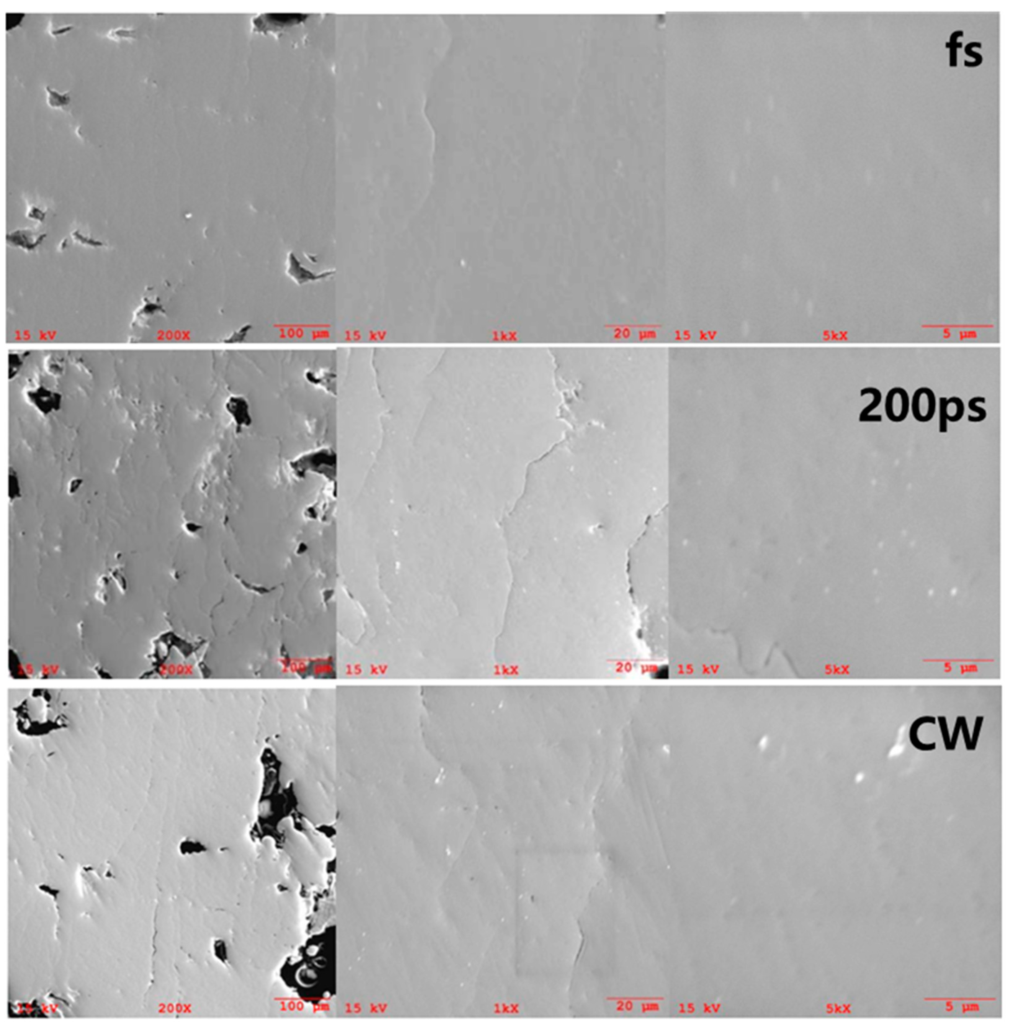
Due to higher power and faster cooling rate, ultrashort pulse laser AM not only reduces the difficulty of forming refractory metals, but also improves the performance of the product by more fully melting and refining grains. Shuang Bai [56] used an SLM experimental device to manufacture tungsten products with different laser pulse widths. The cross-sectional SEM images of the product under different process conditions is shown in Figure 3. It does show that the fs laser-based AM generates less and smaller cracks and defects as compared with those AM parts made with short pulse or CW lasers. And the grain shape and size of the products produced by femtosecond laser and CW laser are also discussed. The results show that the hardness of the products processed by femtosecond laser is better than that of short pulse laser and CW laser, as listed in Table 1. Through the comparison of the process-structure-performance relationship, it can be found that the tungsten samples obtained by the femtosecond laser AM have achieved better results in terms of microstructure and mechanical properties. And through function fitting, it is concluded that the shorter the laser pulse width, the higher the density of the tungsten product and the lower the porosity can be obtained. This is mainly because the melting characteristics (such as melting pool, heating rate, and possible cooling rate) induced by higher peak power of fs laser are much higher in rate and confined (melting pool) than short lasers due to the higher laser intensity and less HAZ.
This work revealed that the fs AM samples had lower cracks and defects compared to the other laser printed samples, which proved that the microstructure or grain size of AM parts can be manipulated or modified via laser parameters. For refractory metals, ultrashort laser have presented great application prospects [57]. However, pores and cracks are still unavoidable, which means that improving process parameters has the potential to further improvements in product performance. In addition to improving the scanning strategy, adding toughness elements to improve the whole product toughness is also a feasible route.

3.2. Transparent Material

Transparent and fragile glass are widely used in semiconductor, energy, communications, biomedicine and aerospace industries due to its high hardness, high chemical and thermal stability, and high transparency of the visible spectrum, making it as a kind of key material in modern society [58]. Due to its high hardness and brittleness, glass is very difficult to be processed via traditional technologies. Moreover, most laser sources have high transmittance to penetrate glass, and nonlinear optical materials have a low energy absorption rate for low power, which makes it difficult to process completely [59]. Compared with CW laser and short laser, the ultrashort pulse laser has the characteristics of high energy peak and low HAZ. When the time between two continuous pulses is much shorter than the characteristic time of thermal diffusion, heat accumulation will cause temperature constant increase. The melting and resolidification mechanism produced by the interaction time between the ultrashort irradiation area and the laser radiation surpasses the traditional thermal equilibrium process. This extremely short solidification time can prevent the segregation of different material components in the molten pool. Therefore, the distribution of different species is more uniform, and the resulting microstructure supports higher mechanical strength, while also having better optical properties [60,61]. Based on the interaction of ultrashort pulse laser nonlinear absorption effect and thermal accumulation effect, the use of ultrashort pulse laser has great potential for nonlinear optical material processing [62].
Literature [33] used a laser pulse with 500 fs pulse width and a center wavelength of 515 nm to melt glass in selected areas to realize the production of porous bulk glass parts, and the structure thickness is less than 30 µm. At repetition rates below the MHz-regime, no formation of molten tracks could be achieved due to insufficient heat accumulation within the powder. A further rise in pulse energy leads to a regime, where glass particles in the focus were ablated/blasted away by single pulses without significant melting of the remaining glass particles. So, it is very important to choose a suitable machining window when consider the interaction of nonlinear absorption and heat accumulation effects. A stable structure exhibiting fully molten tracks with powder sintered to the melt tracks was achieved by adjusting the laser parameters to repetition rate: 20 MHz, pulse energy: 0.55 mJ and scanning velocity: 20 mm/s, corresponding to a line energy of about 575 J/m, as shown in Figure 4a. By using ultrashort pulse induced melting, fabrication of solid cuboids and complex gear wheel structures could be realized, as shown in Figure 4b. Due to the high viscosity of glass, if there are no bubbles wrapped in the glass matrix, it cannot be partially melted. This behavior prevents the evolution of the powder structure to the transparent glass structure during laser processing.
Yttrium stabilized zirconium dioxide (YSZ) has the characteristics of brittleness, light weight, and the tendency of fine particles to agglomerate [63]. Traditional manufacturing method are hardly used to realize to the manufacture of parts with high porosity and special geometric shapes (flat or tubular). Jian Liu [64] used femtosecond laser for laser AM of YSZ, and discussed the influence of laser power and other parameters on the morphology and structure of molten parts. It is shown that increasing the laser power to 131 W and the scanning speed to 300 mm/s can obtain high-quality fully dense thin-layer melting parts with a total area of 20 × 60 mm. The measured micro-hardness is 18.84 GPa and uniform with the density of larger than 99%, which is much higher than the hardness of industrial granulated YSZ solid disk (fuel material of 13.66 GPa).
The above results show that the use of ultrashort pulse laser AM has great potential in the semiconductor and energy industries, and its product performance is significantly improved as compared with the traditional manufacturing methods with a very high local resolution. Ultrashort pulse laser AM is a potential method in the manufacture of composite glass devices, based on the characteristics such as low thermal expansion, chemical inert behavior, or electrical and thermal insulation of optical functional devices. But the current research on the preparation of brittle materials such as transparent and fragile glass by AM methods is still in the exploratory stage, while the samples show a relatively rough surface and porous appearance. The fabricated elements exhibited a porous morphology due to the low-dense source material in combination with the high viscosity of glass. Further improvements regarding the overall density of glass AM parts may be realized with the help of spherical powder grains that support the processing of layers with thicknesses significantly below 50 µm. In actual operations, some problems such as thermal ablation caused by the accumulation of slag and the secondary action of laser light still hinder laser processing from moving towards a more precise processing level, so processing transparent and brittle material powder is still a big challenge in industrial practice [65].

3.3. Multi-Material Layered Structure

Using the advantages of 3D printing, this technology can realize product manufacturing with multiple materials, complex geometries and additional functions [66]. One of the important application scenarios is the AM of composite materials. Due to the layer-by-layer slice manufacturing method, there is no weld that causes stress concentration. This unique combination of multiple metals is better than traditional processes. Since these two materials both start in powder form, a variety of metals that are difficult to combine with traditional methods can be combined more easily by SLM [67]. Because it can control the production material in a single manufacturing operation, which can change performance, such as the functionally graded material manufactured can be locally improved by depositing metal or ceramic materials at a specific location in this way. When these operating processes are selected reasonably, structures and products that have never been seen before can be created [68].
SLM has the advantages that traditional methods are difficult to replace, however, there are still some problems of SLM need to be solved. At present, due to the shortcomings of poor surface finish, low productivity, poor quality control, unrepeatability, limited component size, and limited range of printable materials, only a few AM processes are used in modern manufacturing [69]. For metal materials, various alloys have been proposed [16,70,71]. However, in actual production, the mismatch of material with different cooling rate or thermal expansion coefficient will cause many problems, such as peeling of different layers, thermal effects caused by high power, ablation of low melting point materials on the base layer, and different types problems caused by the formation and distribution of crystal images. The low thermal effect of ultrashort pulse laser can avoid some of the above-mentioned problems. Compared with continuous laser, ultrashort pulse lasers provide the use of heat accumulation that depends on the repetition frequency to control the thermal diffusion in the focal area. Moreover, the extremely short curing time can prevent the segregation of different material components in the molten pool. As a result, the distribution of different materials is more uniform, and the resulting microstructure has higher mechanical strength [15]. And high cooling rate and crucible-free processing help reduce pollution, expand solid solubility and fine microstructure.
Bai [72] used a femtosecond laser to study the laser AM of a multi-material multilayer structure. By adding a thin layer of yttrium-stabilized zirconia (YSZ) and a Ni-YSZ layer, a solid oxide fuel cell (SOFC) was formed. Then a layer of lanthanum strontium manganese (LSM) is added to form a basic three-layer battery, the structure is shown in Figure 5a. The system evaluates the performance of a single fuel cell unit with the best density and porosity parameters such as laser power, scanning speed, and scanning mode. Figure 5b is a photo of the SOFC cells with consistent and uniform three-layered cells. Figure 5c shows that the high strength of Ni–YSZ supporting anode can be achieved with controlled porosity at properly adjusted laser power and scan speed. Through ultra-short pulse, the complex procedures of the traditional process are simplified, and the mechanical performance and product accuracy are improved at the same time.
To successfully fabricating multi-material structures, the hatching space was discussed. The melting effect of YSZ on Ni–YSZ as a function of hatching space was investigated and summarized in Figure 6. When the hatching space is too small, continuous ripple lines in the narrow space can be found. This resulted in more cracks propagating in the cross direction. Consequently, the porosity is large (as shown in Figure 6a,b. When the hatching space is too large, melted lines cannot be formed continuously, resulting in unmelt regions and fractured structure with large porosity (as shown in Figure 6g,h. At the hatching space of 20 μm, large uniformly melted regions with less cracks were found, as shown in Figure 6c–f.
For the first time, a three layered structure was built and demonstrated via AM, and more materials are also conceivable. But the interface strength and uniformity of the YSZ electrolyte thickness, reduction of the Ni–YSZ surface roughness and the LAM integration of the interconnect still need to improve. Meanwhile, connecting two different materials at the same time may bring about not only the advantage of each component, but also some undesired properties, Thus, careful and overall consideration should be taken before combining. Moreover, there are still no small challenges for the hybrid manufacturing of materials with completely different physical properties such as metal-polymer-ceramics.

3.4. High Thermal Conductivity Material

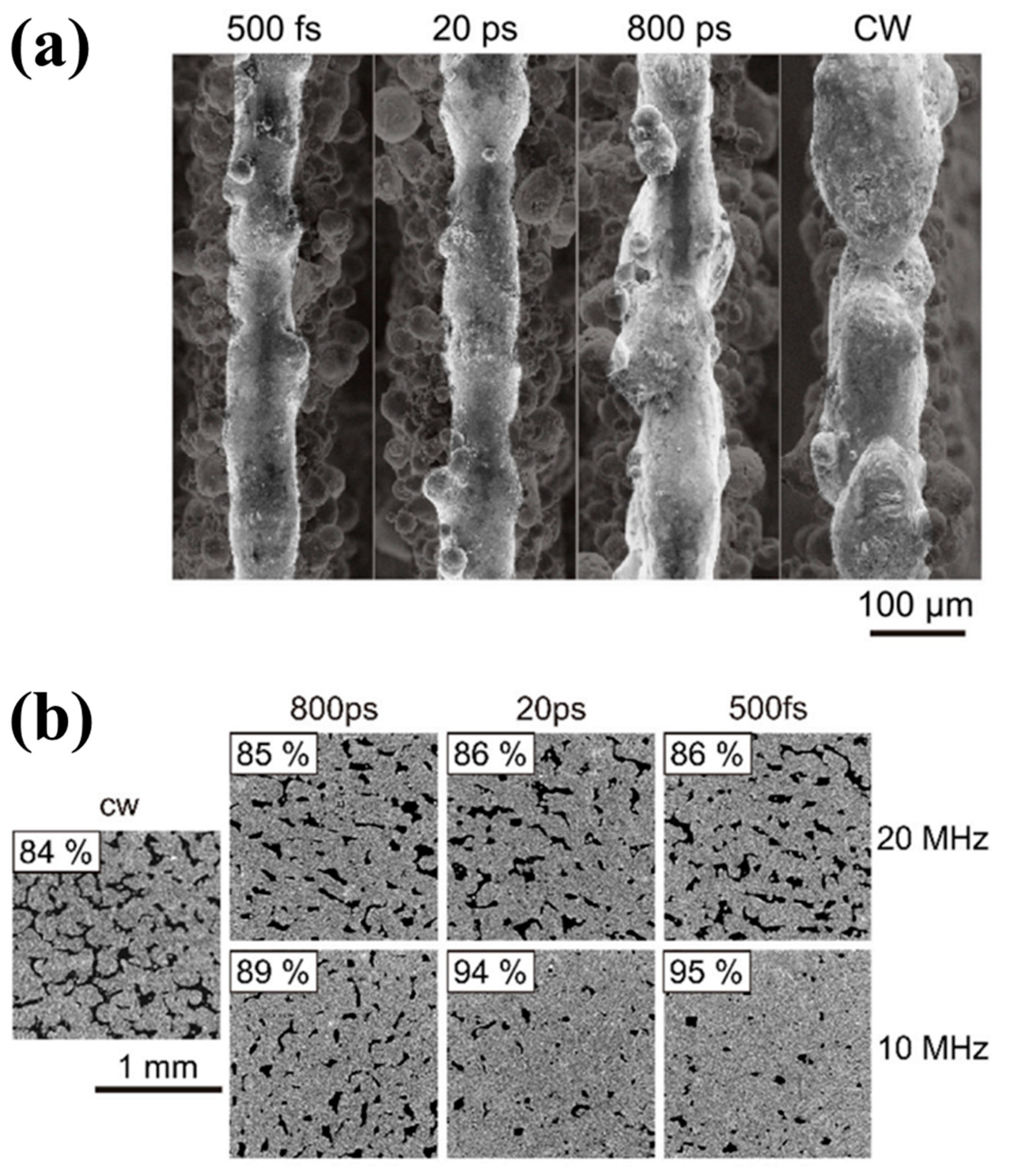
Al-40 Si has special hardness and mechanical strength. However, the achievable cooling rate in the traditional casting process may lead to obvious micro and macro segregation and the formation of brittle δ-AlLi phase [73]. Different from traditional manufacturing processes, SLM results in finer primary Si crystals and more uniform Si distribution due to a faster cooling rate. Compared with CW laser, the pulses of ultrashort pulse laser are shorter, resulting in a molten pool width of less than 100µm, faster heat extraction from the molten pool, finer structure, and better mechanical properties. For this reason, literature [15] studied the influence of pulse width and pulse energy on the size and shape of the Al-40 Si molten pool in the SLM process. In Figure 7a the top view of fused walls with a total height of 4 mm using a scan speed of 200 mm/s and a layer height of 15 µm were shown for different pulse modes in comparison to CW. With increasing pulse duration, the melt pool width increased combined with a reduced uniformity along the scanned path. It was found that the use of 500 fs laser pulses can significantly reduce the porosity, and at higher pulse energy and shorter pulse duration, the relative density of the resulting bulk sample increases while being significantly higher than that of CW as shown in Figure 7b. Therefore, the ultrashort pulse laser pulse shows a huge heat source potential in the high-precision laser powder bed smelting of Al-Si alloys [74].
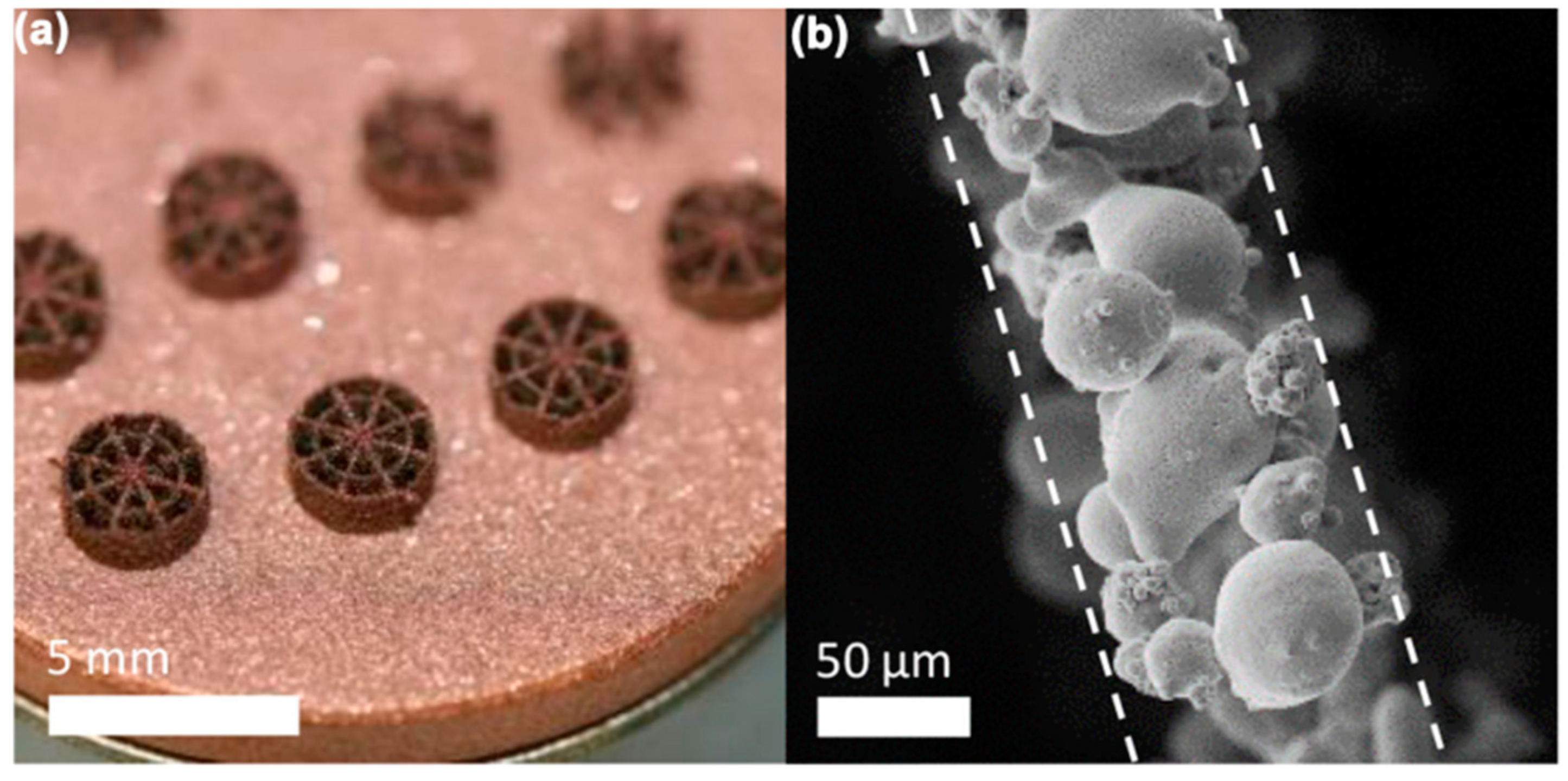
Copper as a metal with high reflectivity and high thermal conductivity (400 W/(mK)) further promotes the dissipation of heat, hinders the temperature rise and affects the shape of the molten pool [75]. And through the heat accumulation at the repetition frequency, the heat diffusion in the focal area is controlled. The ultra-short melting and resolidification process avoids the segregation of crystal images, so that the distribution of different materials is uniform and the final mechanical properties are improved. Literature [76,77] studies the effects of different pulse energies, different repetition frequencies and scanning speeds on the performances of the structure, as shown in Figure 8. This study shows that for a repetition frequency of 200 kHz, solid interconnection with the substrate cannot be achieved. After increasing the pulse frequency to the MHz range, this behavior changed. The 20 MHz processing window was determined by the surface sintering behavior under pulse energy below 0.75 μJ and the ablation effect of pulse energy above 1.5 μJ. Therefore, at 20 MHz and a pulse energy of about 1 μJ, a rough processing window can be identified. On the one hand, it shows the firm connection between the first floor and the building platform, and on the other hand, it involves the firm melting in the layer system. Assuming a spot diameter of 35 μm, this corresponds to a peak flux range of 0.04 to 0.06 J/cm2. When the line energy exceeds 100 J/m, the HAZ is greatly expanded, which will result in a decrease in processing resolution and geometric accuracy.
As mentioned above, the ultra-high thermal conductivity counteracts the induced melting process, allowing the heat to quickly dissipate into the bulk. Basic research has revealed the importance of using high pulse repetition rates for heat accumulation in the MHz range, demonstrating the advantages of ultrashort pulse laser over continuous laser. Furthermore, in the process of SLM high thermal conductivity materials, using its ultra-short melting and resolidification process to improve melting and reduce residual stress has great potential.
Finally, we summarized the most suitable ultrashort pulse laser processing parameters and their material properties in the above-mentioned literature of the special materials, hoping to provide guidance for subsequent industrial production, as shown in Table 2.

4. Summary and Conclusions

Laser additive manufacturing has become a commanding height of future technology and industry due to its innate technical characteristics. The majority of current research efforts considering the SLM process has been carried out with CW and short laser, while ultrafast lasers exhibit better performance. This article discusses the interaction process between ultrashort pulse laser and material, and summarizes the ultrashort pulse laser forming manufacturing in the current ultrashort pulse laser forming process of four special processing fields. The process of interaction between ultrafast laser and materials reaches from the femtosecond to the nanosecond scale, i.e. from the initial energy absorption to the final material removal. Comparing fs laser sintered parts with CW laser and short laser AM parts, it was found that the defects present in fs laser AM samples were fewer compared to other types of lasers. Further fs laser produced greater hardness and higher density parts as compared to CW laser sintered parts. SLM of pure borosilicate glass parts by using ultrashort laser pulses was achieved. A three-layered structure, as a basic cell unit of SOFC, was built and demonstrated via fs AM. It showed that the density and porosity can be well controlled during the fs AM process, and that the basic SOFC cell sample functions. CW and short pulse laser failed to achieve copper parts at the micron or submicron levels because of HAZs, the use of fs laser clearly alleviated the limitation. Based on the research status, the following conclusions suggestions are required to be further considered, before the ultrashort pulse laser forming manufacturing can be practically applied into industrial use:
(1)
The fs laser-based melting process enhances the material processing library of traditional techniques based on CW or short pulse lasers by adding full control over the processing parameters. In particular, challenging materials such as copper, YSZ and tungsten have been reported to produce standard functional parts that meet the requirements of many applications. In addition to the current material, materials with high melting points or brittleness that are difficult to manufacture by traditional methods, such as high-entropy alloys and ceramics, are also worth a try. The potential benefits of fs-AM can be exploited in a wide range of applications due to its high power and low HAZ. Guiding experiments and production through numerical simulation is the focus of future research. The rapid development and application of big data and large-scale parallel computing provide possibilities for process modeling and analysis. With the development of artificial intelligence technology, in the future, through data collection, data processing, machine learning and neural network methods to obtain a reliable process-structure-performance relationship for the SLM process is also an effective way to shorten the calculation time and improve the accuracy of the calculation.
(2)
At present, systematic experiments are mainly carried out on laser power, scanning speed, scanning method, etc. to obtain the process parameters for the best target performance. The parameters involved are numerous, as they are related to materials, laser and the process itself, all of which can affect the performance and quality of the processed parts. This method is time-consuming and labor intensive, and the acquisition of ideal parameters depends on the setting of windows and gradients, which may not suitable as global optimal results. It may only be the local optimum in the set parameters, which also shows that the performance of manufactured parts has the potential for further improvement. As tungsten parts have been successfully fabricated with fs laser sources, microcracks are still prevalent. The next step is to continue to strengthen the process optimization research of fs SLM, especially the intelligent process optimization based on computer numerical calculation technology. While the rapid heating and cooling associated with ultrafast laser processing helps to homogenize the composition and prevent segregation, it also creates residual stress and affects the performance of the fabricated part, and SLM-based products still suffer from surface finish defects, so post-processing is needed. At the same time, expensive powder preparation and other costs are also factors that must be considered for the use of this technique.
(3)
Although the current rapid development of AM, there are still problems in actual experimental operations, such as limited size of printed samples and long printing time. At the same time, there are problems such as complex and expensive powder preparation. It is also necessary to speed up the research and development of additive manufacturing equipment. At present, many of fs-SLM are based on the transformation and upgrading of traditional CW laser SLM equipment. There are many limitations, and there is still a lack of market-oriented mature printing equipment sales. The next step is to accelerate the research in this area, especially the research and development of high-performance lasers and optical path systems suitable for the fs SLM process.

Author Contributions

Conceptualization, formal analysis, original draft preparation, writing, Y.W.; review and editing, L.K. and Y.C.; investigation, Z.J. and X.L. All authors have read and agreed to the published version of the manuscript.

Funding

This research received no external funding.

Data Availability Statement

Not applicable.

Conflicts of Interest

The authors declare that they have no known competing financial interests or personal relationships that could have appeared to influence the work reported in this paper.

References

  1. Cao, L. Mesoscopic-scale numerical investigation including the influence of scanning strategy on selective laser melting process. Comput. Mater. Sci. 2021, 189, 110263. [Google Scholar] [CrossRef]
  2. Lonergan, J.; Fahrenholtz, W.; Hilmas, G. Zirconium Diboride with High Thermal Conductivity. J. Am. Ceram. Soc. 2014, 97, 1689–1691. [Google Scholar] [CrossRef]
  3. Gieseke, M.; Senz, V.; Vehse, M.; Fiedler, S.; Irsig, R.; Hustedt, M.; Sternberg, K.; Noelke, C.; Kaierle, S.; Wesling, V.; et al. Additive Manufacturing of Drug Delivery Systems. Biomed. Technik. Biomed. Eng. 2012, 57, 398–401. [Google Scholar] [CrossRef]
  4. Chichkov, B.N.; Momma, C.; Nolte, S.; von Alvensleben, F.; Tünnermann, A. Femtosecond, picosecond and nanosecond laser ablation of solids. Appl. Phys. A 1996, 63, 109–115. [Google Scholar] [CrossRef]
  5. Noël, S.; Hermann, J.; Itina, T. Investigation of nanoparticle generation during femtosecond laser ablation of metals. Appl. Surf. Sci. 2007, 253, 6310–6315. [Google Scholar] [CrossRef]
  6. Chowdhury, I.; Xu, X. Heat Transfer in Femtosecond Laser Processing of Metal. Numer. Heat Transf. Part A-Appl. 2003, 44, 219–232. [Google Scholar] [CrossRef]
  7. Lei, S.; Zhao, X.; Yu, X.; Hu, A.; Vukelic, S.; Jun, M.; Joe, H.-E.; Yao, Y.; Shin, Y. Ultrafast Laser Applications in Manufacturing Processes: A State of the Art Review. J. Manuf. Sci. Eng. 2020, 142, 031005. [Google Scholar] [CrossRef]
  8. Birnbaum, M. Semiconductor Surface Damage Produced by Ruby Lasers. J. Appl. Phys. 1965, 36, 3688–3689. [Google Scholar] [CrossRef]
  9. Hodgson, N.; Laha, M.; Lee, T.; Haloui, H.; Heming, S.; Steinkopff, A. Industrial Ultrafast Lasers Systems, Processing Fundamentals, and Applications. In Proceedings of the 2019 Conference on Lasers and Electro-Optics (CLEO), San Jose, CA, USA, 5–10 May 2019. [Google Scholar]
  10. Xiao, K.; Li, M.; Li, M.; Dai, R.; Hou, Z.; Qiao, J. Femtosecond laser ablation of AZ31 magnesium alloy under high repetition frequencies. Appl. Surf. Sci. 2022, 594, 153406. [Google Scholar] [CrossRef]
  11. Chen, C.; Zhang, F.; Zhang, Y.; Xiong, X.; Ju, B.-F.; Cui, H.; Chen, Y.-L. Single-pulse femtosecond laser ablation of monocrystalline silicon: A modeling and experimental study. Appl. Surf. Sci. 2022, 576, 151722. [Google Scholar] [CrossRef]
  12. Roth, G.-L.; Rung, S.; Hellmann, R. Welding of transparent polymers using femtosecond laser. Appl. Phys. A-Mater. Sci. Process. 2016, 122, 86. [Google Scholar] [CrossRef]
  13. Tamaki, T.; Watanabe, W.; Nishii, J.; Itoh, K. Welding of transparent materials using femtosecond laser pulses. Jpn. J. Appl. Phys. Part 2-Lett. Express Lett. 2005, 44, L687–L689. [Google Scholar] [CrossRef]
  14. Li, X.; Jing, F.; Fan, J.; Yong, P.; Wang, K. Parametric investigation of femtosecond laser welding on alumina using Taguchi technique. Optik 2021, 225, 165891. [Google Scholar] [CrossRef]
  15. Ullsperger, T.; Liu, D.; Yürekli, B.; Matthäus, G.; Schade, L.; Seyfarth, B.; Kohl, H.; Ramm, R.; Rettenmayr, M.; Nolte, S. Ultra-short pulsed laser powder bed fusion of Al-Si alloys: Impact of pulse duration and energy in comparison to continuous wave excitation. Addit. Manuf. 2021, 46, 102085. [Google Scholar] [CrossRef]
  16. Aversa, A.; Marchese, G.; Saboori, A.; Bassini, E.; Manfredi, D.; Biamino, S.; Ugues, D.; Fino, P.; Lombardi, M. New Aluminum Alloys Specifically Designed for Laser Powder Bed Fusion: A Review. Materials 2019, 12, 1007. [Google Scholar] [CrossRef] [Green Version]
  17. Raciukaitis, G. Ultra-Short Pulse Lasers for Microfabrication: A Review. IEEE J. Sel. Top. Quantum Electron. 2021, 27, 1–12. [Google Scholar] [CrossRef]
  18. von der Linde, D.; Sokolowski-Tinten, K.; Bialkowski, J. Laser–solid interaction in the femtosecond time regime. Appl. Surf. Sci. 1997, 109–110, 1–10. [Google Scholar] [CrossRef]
  19. Kabotu, K.; Samuel, G.L.; Shunmugam, M.s. Theoretical and experimental Investigations of Ultra-short Pulse Laser Interaction on Ti6Al4V alloy. J. Mater. Process. Technol. 2018, 263, 266–275. [Google Scholar] [CrossRef]
  20. Wu, B.; Shin, Y. A simple model for high fluence ultra-short pulsed laser metal ablation. Appl. Surf. Sci. 2007, 253, 4079–4084. [Google Scholar] [CrossRef]
  21. Wellershoff, S.; Hohlfeld, J.; Güdde, J.; Matthias, E. The role of electron-phonon coupling in femtosecond laser damage of metals. Appl. Phys. A 1999, 69, S99–S107. [Google Scholar] [CrossRef]
  22. Li, X.; Guan, Y. Theoretical fundamentals of short pulse laser–metal interaction: A review. Nanotechnol. Precis. Eng. 2020, 3, 105–125. [Google Scholar] [CrossRef]
  23. Corkum, P.B.; Brunel, F.; Sherman, N.K.; Srinivasan-Rao, T. Thermal Response of Metals to Ultrashort-Pulse Laser Excitation. Phys. Rev. Lett. 1988, 61, 2886–2889. [Google Scholar] [CrossRef] [PubMed]
  24. Gusarov, A.V.; Yadroitsev, I.; Bertrand, P.; Smurov, I. Model of Radiation and Heat Transfer in Laser-Powder Interaction Zone at Selective Laser Melting. J. Heat Transf. 2009, 131, 072101. [Google Scholar] [CrossRef]
  25. Le Harzic, R.; Breitling, D.; Weikert, M.; Sommer, S.; Föhl, C.; Valette, S.; Donnet, C.; Audouard, E.; Dausinger, F. Pulse width and energy influence on laser micromachining of metals in a range of 100 fs to 5 ps. Appl. Surf. Sci. 2005, 249, 322–331. [Google Scholar] [CrossRef]
  26. Yang, J.; Zhao, Y.; Zhu, X. Theoretical studies of ultrafast ablation of metal targets dominated by phase explosion. Appl. Phys. A 2007, 89, 571–578. [Google Scholar] [CrossRef]
  27. Rethfeld, B.; Ivanov, D.S.; Garcia, M.E.; Anisimov, S.I. Modelling ultrafast laser ablation. J. Phys. D: Appl. Phys. 2017, 50, 193001. [Google Scholar] [CrossRef]
  28. Anisimov, S.I.; Relhfeld, B. On the theory of ultrashort laser pulse interaction with a metal. Nauk Fiz 1997, 61, 1642–1655. [Google Scholar]
  29. Wang, X.L.; Wu, H.; Chang, Y.X.; Zhu, W.H.; Chen, Z.Y.; Lu, P.X. Influence of thermophysical parameters by femtosecond laser ablation of metals: Molecular dynamics simulation. Guangzi Xuebao/Acta Photonica Sin. 2009, 38, 3052–3056. [Google Scholar]
  30. Iartsev, B.; Vichev, I.; Tsygvintsev, I.; Sidelnikov, Y.; Krivokorytov, M.; Medvedev, V. On experimental and numerical study of the dynamics of a liquid metal jet hit by a laser pulse. Exp. Fluids 2020, 61, 119. [Google Scholar] [CrossRef]
  31. Zhu, G.; Xu, Z.; Jin, Y.; Chen, X.; Yang, L.; Xu, J.; Shan, D.; Chen, Y.; Guo, B. Mechanism and application of laser cleaning: A review. Opt. Lasers Eng. 2022, 157, 107130. [Google Scholar] [CrossRef]
  32. Kerse, C.; Kalaycioglu, H.; Elahi, P.; Cetin, B.; Kesim, D.K.; Akcaalan, O.; Yavas, S.; Asik, M.D.; Oktem, B.; Hoogland, H.; et al. Ablation-cooled material removal with ultrafast bursts of pulses. NATURE 2016, 537, 84–88. [Google Scholar] [CrossRef] [PubMed]
  33. Seyfarth, B.; Schade, L.; Ullsperger, T.; Matthäus, G.; Tünnermann, A.; Nolte, S. Selective Laser Melting of Borosilicate Glass Using Ultrashort Laser Pulses. Available online: https://www.spiedigitallibrary.org/conference-proceedings-of-spie/10523/105230C/Selective-laser-melting-of-glass-using-ultrashort-laser-pulses/10.1117/12.2289614.short?SSO=1 (accessed on 13 October 2022).
  34. Stuart, B.C.; Feit, M.D.; Herman, S.; Rubenchik, A.M.; Shore, B.W.; Perry, M.D. Nanosecond-to-femtosecond laser-induced breakdown in dielectrics. PHYSICAL REVIEW B 1996, 53, 1749–1761. [Google Scholar] [CrossRef] [PubMed]
  35. Lizunov, S.A.; Bulgakov, A.V.; Campbell, E.E.B.; Bulgakova, N.M. Melting of gold by ultrashort laser pulses: Advanced two-temperature modeling and comparison with surface damage experiments. Appl. Phys. A 2022, 128, 602. [Google Scholar] [CrossRef]
  36. Xie, J.; Yan, J.; Zhu, D. Atomic simulation of irradiation of Cu film using femtosecond laser with different pulse durations. J. Laser Appl. 2020, 32, 022016. [Google Scholar] [CrossRef] [Green Version]
  37. Zhou, Y.; Wu, D.; Luo, G.; Hu, Y.; Qin, Y. Efficient modeling of metal ablation irradiated by femtosecond laser via simplified two-temperature model coupling molecular dynamics. J. Manuf. Process. 2022, 77, 783–793. [Google Scholar] [CrossRef]
  38. Colombier, J.P.; Combis, P.; Bonneau, F.; Le Harzic, R.; Audouard, E. Hydrodynamic simulations of metal ablation by femtosecond laser irradiation. Phys. Rev. B 2005, 71, 165406. [Google Scholar] [CrossRef] [Green Version]
  39. Qiu, T.Q.; Tien, C.L. Heat-Transfer Mechanisms during Short-Pulse Laser-Heating of Metals. J. Heat Transf. -Trans. Same 1993, 115, 835–841. [Google Scholar] [CrossRef]
  40. Zhu, D.; Yan, J.; Xie, J.; Liang, Z.; Bai, H. Ultrafast Laser-Induced Atomic Structure Transformation of Au Nanoparticles with Improved Surface Activity. ACS Nano 2021, 15, 13140–13147. [Google Scholar] [CrossRef]
  41. Xie, J.; Yan, J.; Zhu, D.; He, G. Atomic-Level Insight into the Formation of Subsurface Dislocation Layer and Its Effect on Mechanical Properties During Ultrafast Laser Micro/Nano Fabrication. Adv. Funct. Mater. 2022, 32, 2108802. [Google Scholar] [CrossRef]
  42. Meng, Y.; Ji, P.; Jiang, L.; Lin, G.; Guo, J. Spatiotemporal insights into the femtosecond laser homogeneous and heterogeneous melting aluminum by atomistic-continuum modeling. Appl. Phys. A 2022, 128, 520. [Google Scholar] [CrossRef]
  43. Panwisawas, C.; Qiu, C.; Anderson, M.J.; Sovani, Y.; Turner, R.P.; Attallah, M.M.; Brooks, J.W.; Basoalto, H.C. Mesoscale modelling of selective laser melting: Thermal fluid dynamics and microstructural evolution. Comput. Mater. Sci. 2017, 126, 479–490. [Google Scholar] [CrossRef]
  44. Khairallah, S.; Anderson, A.; Rubenchik, A.; King, W. Laser powder-bed fusion additive manufacturing: Physics of complex melt flow and formation mechanisms of pores, spatter, and denudation zones. Acta Mater. 2016, 108, 36–45. [Google Scholar] [CrossRef]
  45. Yang, M.; Wang, L.; Yan, W. Phase-field modeling of grain evolution in additive manufacturing with addition of reinforcing particles. Addit. Manuf. 2021, 47, 102286. [Google Scholar] [CrossRef]
  46. Kruth, J.-P.; Froyen, L.; Vaerenbergh, J.; Mercelis, P.; Rombouts, M.; Lauwers, B. Selective laser melting of iron-based powder. J. Mater. Process. Technol. 2004, 149, 616–622. [Google Scholar] [CrossRef]
  47. Lassner, E. Tungsten: Properties, Chemistry, Technology of the Element, Alloys, and Chemical Compounds. 2000. Available online: https://onlinelibrary.wiley.com/doi/10.1002/14356007.a27_229 (accessed on 13 October 2022).
  48. Duriagina, Z.; Kulyk, V.; Kovbasiuk, T.; Vasyliv, B.; Kostryzhev, A. Synthesis of Functional Surface Layers on Stainless Steels by Laser Alloying. Metals 2021, 11, 434. [Google Scholar] [CrossRef]
  49. Zhou, Z.; Pintsuk, G.; Linke, J.; Hirai, T.; Rödig, M.; Ma, Y.; Ge, C. Transient high heat load tests on pure ultra-fine grained tungsten fabricated by resistance sintering under ultra-high pressure. Fusion Eng. Des. 2010, 85, 115–121. [Google Scholar] [CrossRef]
  50. Ma, J.; Zhang, J.; Liu, W.; Shen, Z. Suppressing pore-boundary separation during spark plasma sintering of tungsten. J. Nucl. Mater. 2013, 438, 199–203. [Google Scholar] [CrossRef]
  51. Wang, D.; Yu, C.; Zhou, X.; Ma, J.; Liu, W.; Shen, Z. Dense Pure Tungsten Fabricated by Selective Laser Melting. Appl. Sci. 2017, 7, 430. [Google Scholar] [CrossRef]
  52. Ebert, R.; Ullmann, F.; Hildebrandt, D.; Schille, J.; Hartwig, L.; Klötzer, S.; Streek, A.; Exner, H. Laser Processing of Tungsten Powder with Femtosecond Laser Radiation. JLMN-J. Laser Micro/Nanoeng. 2012, 7, 38–43. [Google Scholar] [CrossRef]
  53. Zhang, D.; Cai, Q.; Liu, J. Formation of Nanocrystalline Tungsten by Selective Laser Melting of Tungsten Powder. Mater. Manuf. Process. 2012, 27, 1267–1270. [Google Scholar] [CrossRef]
  54. Zhou, X.; Liu, X.; Zhang, D.; Shen, Z.; Liu, W. Balling phenomena in selective laser melted tungsten. J. Mater. Process. Technol. 2015, 222, 33–42. [Google Scholar] [CrossRef]
  55. Bai, S.; Liu, J.; Yang, P.; Huang, H.; Yang, L.-M. Femtosecond fiber laser additive manufacturing of tungsten. Laser 3d Manuf. III 2016, 9738, 96–105. [Google Scholar]
  56. Bai, S.; Yang, L.; Liu, J. Manipulation of microstructure in laser additive manufacturing. Appl. Phys. A 2016, 122, 495. [Google Scholar] [CrossRef]
  57. Zhang, H.; Zhao, Y.; Huang, S.; Zhu, S.; Wang, F. Manufacturing and Analysis of High-Performance Refractory High-Entropy Alloy via Selective Laser Melting (SLM). Materials 2019, 12, 720. [Google Scholar] [CrossRef] [PubMed] [Green Version]
  58. Komatsu, T.; Honma, T. Laser patterning and growth mechanism of orientation designed crystals in oxide glasses: A review. J. Solid State Chem. 2019, 275, 210–222. [Google Scholar] [CrossRef]
  59. Minghui, H.; Koji, S.; Yongfeng, L.; Katsumi, M.; Tow Chong, C. Optical Diagnostics in Laser-Induced Plasma-Assisted Ablation of Fused Quartz. Available online: https://www.spiedigitallibrary.org/conference-proceedings-of-spie/4088/0000/Optical-diagnostics-in-laser-induced-plasma-assisted-ablation-of-fused/10.1117/12.405763.short?SSO=1 (accessed on 13 October 2022).
  60. Xia, Y.; Jing, X.; Zhang, D.; Wang, F.; Jaffery, S.; Li, H. A comparative study of direct laser ablation and laser-induced plasma-assisted ablation on glass surface. Infrared Phys. Technol. 2021, 115, 103737. [Google Scholar] [CrossRef]
  61. Seyfarth, B.; Schade, L.; Matthäus, G.; Ullsperger, T.; Heidler, N.; Hilpert, E.; Nolte, S. Laser powder bed fusion of glass: A comparative study between CO2 lasers and ultrashort laser pulses. Laser 3D Manuf. VII 2020, 11271, 87–92. [Google Scholar]
  62. Liu, J.; Deng, C.; Bai, S. Glass surface metal deposition with high-power femtosecond fiber laser. Appl. Phys. A 2016, 122, 1064. [Google Scholar] [CrossRef]
  63. Huang, W.L.; Zhu, Q.; Xie, Z. Gel-cast anode substrates for solid oxide fuel cells. J. Power Sources 2006, 162, 464–468. [Google Scholar] [CrossRef]
  64. Liu, J.; Bai, S. Femtosecond laser additive manufacturing of YSZ. Appl. Phys. A 2017, 123, 293. [Google Scholar] [CrossRef]
  65. Zhang, Z.; Yang, Z.; Wang, C.; Zhang, Q.; Zheng, S.; Xu, W. Mechanisms of femtosecond laser ablation of Ni3Al: Molecular dynamics study. Opt. Laser Technol. 2021, 133, 106505. [Google Scholar] [CrossRef]
  66. Huang, S.; Liu, P.; Mokasdar, A.; Liang, H. Additive manufacturing and its societal impact: A literature review. Int. J. Adv. Manuf. Technol. 2012, 67, 1191–1203. [Google Scholar] [CrossRef]
  67. Bandyopadhyay, A.; Heer, B. Additive manufacturing of multi-material structures. Mater. Sci. Eng. R Rep. 2018, 129, 1–16. [Google Scholar] [CrossRef]
  68. Cui, J.; Ren, L.; Mai, J.; Zheng, P.; Zhang, L. 3D Printing in the Context of Cloud Manufacturing. Robot. Comput. -Integr. Manuf. 2022, 74, 102256. [Google Scholar] [CrossRef]
  69. Heemsbergen, L.; Daly, A.; Lu, J.; Birtchnell, T. 3D-printed Futures of Manufacturing, Social Change and Technological Innovation in China and Singapore: The Ghost of a Massless Future? Sci. Technol. Soc. 2019, 24, 254–270. [Google Scholar] [CrossRef]
  70. Ullsperger, T.; Matthäus, G.; Kaden, L.; Engelhardt, H.; Rettenmayr, M.; Risse, S.; Tünnermann, A.; Nolte, S. Selective laser melting of hypereutectic Al-Si40-powder using ultra-short laser pulses. Appl. Phys. A 2017, 123, 798. [Google Scholar] [CrossRef] [Green Version]
  71. Gorsse, S.; Hutchinson, C.; Goune, M.; Banerjee, R. Additive manufacturing of metals: A brief review of the characteristic microstructures and properties of steels, Ti-6Al-4V and high-entropy alloys. Sci. Technol. Adv. Mater. 2017, 18, 584–610. [Google Scholar] [CrossRef] [Green Version]
  72. Bai, S.; Liu, J. Femtosecond Laser Additive Manufacturing of Multi-Material Layered Structures. Appl. Sci. 2020, 10, 979. [Google Scholar] [CrossRef] [Green Version]
  73. Dursun, T.; Soutis, C. Recent developments in advanced aircraft aluminium alloys. Mater. Des. 2014, 56, 862–871. [Google Scholar] [CrossRef]
  74. Grigoriev, S.; Tarasova, T.; Gvozdeva, G. Optimization of Parameters of Laser Surfacing of Alloys of the Al–Si System. Met. Sci. Heat Treat. 2016, 57, 589–595. [Google Scholar] [CrossRef]
  75. Cheng, C.; Chen, J. Femtosecond laser sintering of copper nanoparticles. Appl. Phys. A 2016, 122, 289. [Google Scholar] [CrossRef]
  76. Kaden, L.; Matthäus, G.; Ullsperger, T.; Engelhardt, H.; Rettenmayr, M.; Tünnermann, A.; Nolte, S. Selective laser melting of copper using ultrashort laser pulses. Appl. Phys. A 2017, 123, 596. [Google Scholar] [CrossRef]
  77. Kaden, L.; Seyfarth, B.; Ullsperger, T.; Matthäus, G.; Nolte, S. Selective Laser Melting of Copper Using Ultrashort Laser Pulses at Different Wavelengths. 2018, p. 41. Available online: https://www.semanticscholar.org/paper/Selective-laser-melting-of-copper-using-ultrashort-Kaden-Matth%C3%A4us/073040f72798f8047864da3ee38cd1769c61319f#citing-papers (accessed on 13 October 2022). [CrossRef]
  78. Nie, B.; Huang, H.; Bai, S.; Liu, J. Femtosecond laser melting and resolidifying of high-temperature powder materials. Appl. Phys. A 2015, 118, 37–41. [Google Scholar] [CrossRef]
  79. Nie, B.; Yang, L.; Huang, H.; Bai, S.; Wan, P.; Liu, J. Femtosecond laser additive manufacturing of iron and tungsten parts. Appl. Phys. A 2015, 119, 1075–1080. [Google Scholar] [CrossRef]
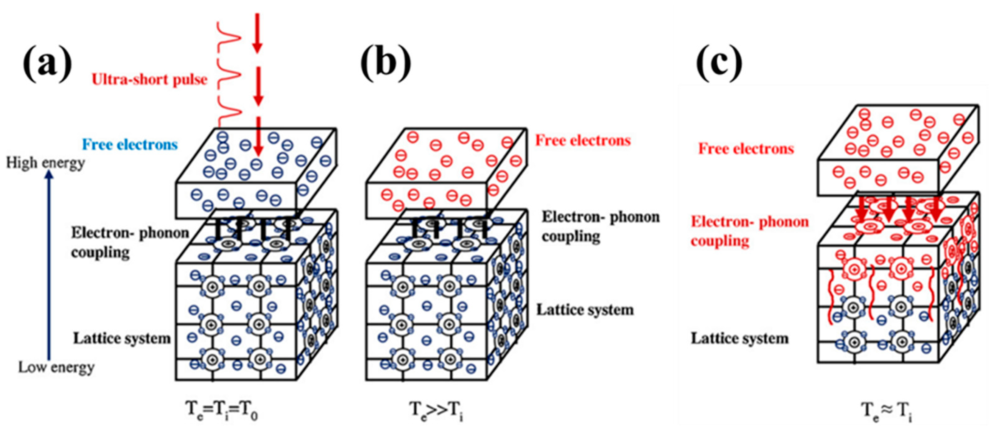
Figure 1. Mechanism of interaction between ultrashort pulse laser and materials (Te-electron temperature, Ti-lattice temperature, T0-ambient temperature). (a) absorption. (b) Heating. (c) Energy transfer [19].
Crystals 12 01480 g001
Figure 2. Typical timescales and intensity ranges of several phenomena and processes occurring during and after irradiation of a solid with an ultrashort laser pulse of about 100 fs duration [27].
Crystals 12 01480 g002
Figure 3. Cross section of tungsten sample, from top to bottom, made by fs,200 ps and CW; from left to right, SEM image of ×200, ×1000, ×5000 [56].
Crystals 12 01480 g003
Figure 4. (a) SEM image (top view) of a fabricated cubic sample, exhibiting molten tracks and gas inclusions due to the high viscosity of glass. (b) Fabricated gear wheel with dimensions of 10.5 mm in diameter and 1.5 mm height [33].
Crystals 12 01480 g004
Figure 5. (a) Solid oxide fuel cell (SOFC) design architecture. A single cell unit include cathode (LSM), electrolyte (YSZ), and anode (Ni–YSZ), air is supplied to the cathode surface whereas fuel is supplied to the anode surface. (b) Complete three-layered cell samples (30 × 30 mm). (c) cross-section SEM image of the interfaces for a complete cell sample [72].
Crystals 12 01480 g005
Figure 6. Microscopic images (different scales) of the YSZ layer printed on the Ni–YSZ anode substrates. (a,b) Hatching space of 15 μm, scanning speed of 80 mm/s, and target power of 78 W. (c,d) hatching space of 20 μm, scanning speed of 100 mm/s, and target power of 78 W. (e,f) Hatching space of 20 μm, scanning speed of 80 mm/s, and target power of 78 W. (g,h) Hatching space of 25 μm, scanning speed of 100 mm/s, and target power of 78 W [72].
Crystals 12 01480 g006
Figure 7. (a) SEM images of walls (top view) produced at different pulse width. (b)The corresponding relative densities of the samples produced using different pulse durations and repetition rates obtained by X-ray CT [15].
Crystals 12 01480 g007
Figure 8. (a)Typical sample of thin-wall structures with diameter of 3 mm processed with different laser parameter sets. (b) SEM image of a single wall with a thickness below 100 μm, which is marked by the dashed lines. A pulse energy of 1.0 μJ and scan velocity 666 mm/s was applied [64].
Crystals 12 01480 g008
Table 1. Summary of the hardness testing results for different samples [56].
Hardness (HRC)Fs20 ps200 psCWTungsten Substrate
Top45.444.142.444.744.9
Cross section47.741.8 45.144.945.8
Table 2. The suitable ultrashort pulse laser processing parameters and material properties.
MaterialPower (W)Pulse Repetition Frequency (MHZ)Energy (µJ)Pulse Width (fs)Scan Speed (mm/s)Peak Power (MW)Melting Point
(°C)
Thermal
Conductivity
(W/(m × k))
rhenium [78]50122.54002056.253250
Tungsten [79]50150400251253422174
iron [64]50800.625350501.791538173
Borosilicateglass [33]11200.55900200.575 0.8–1
YSZ [64]131801.6388003002.05 1.8
YSZ layer on substrate [72]78800.9758001001.22
Al-Si
alloy [12]
25201.25500 2.5 121–151
copper [76]2020150066621084400
Publisher’s Note: MDPI stays neutral with regard to jurisdictional claims in published maps and institutional affiliations.