
Single-Step Fabrication and Characterization of Nanoscale Cu Thinfilms for Optoelectronic Applications

 ,
,  , ,
, ,  ,
,
Abstract
:1. Introduction
2. Experimental Work
2.1. Substrate Cleaning
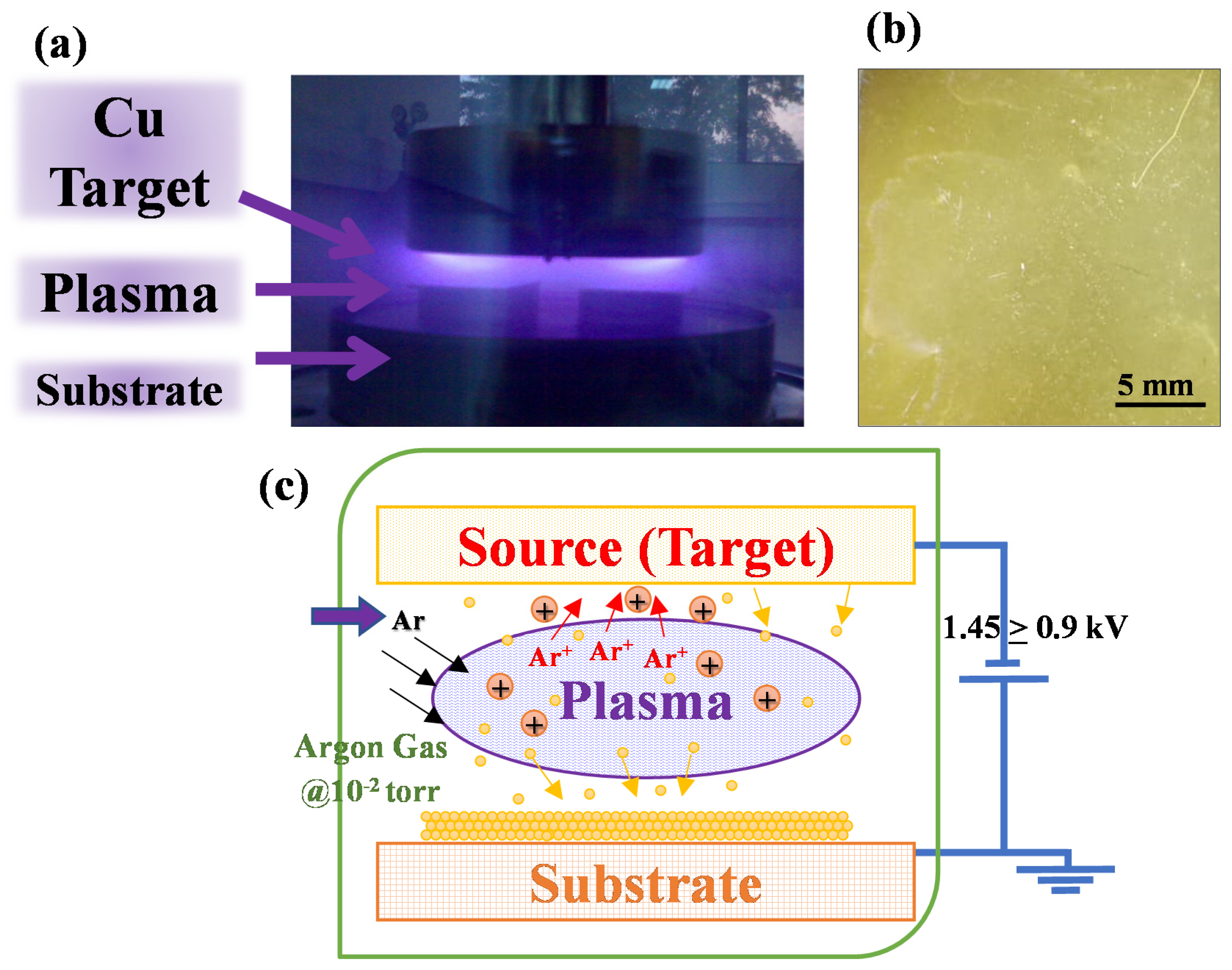
2.2. Sputtering of Copper
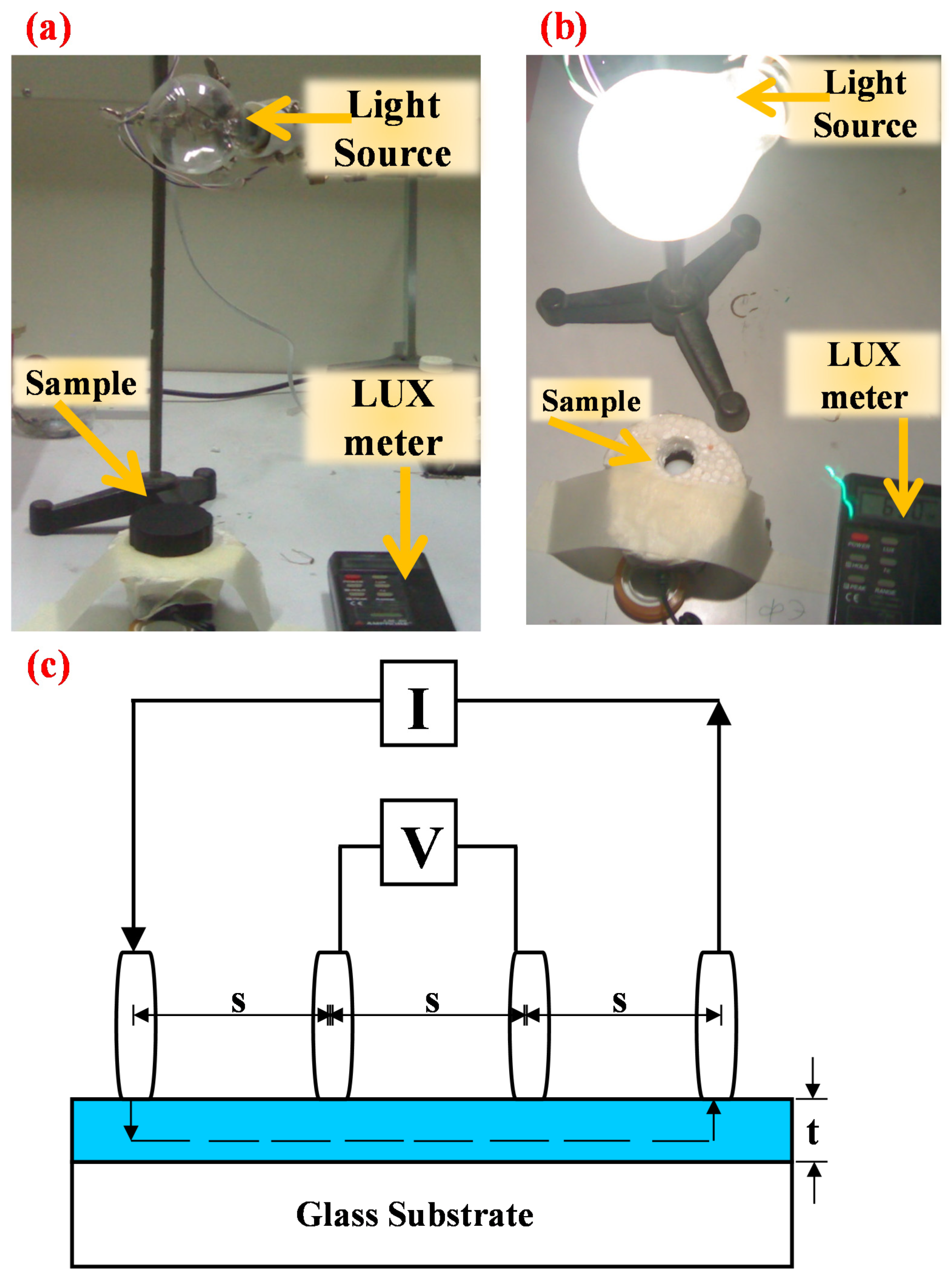
2.3. Light Transmittance of Copper Nano-Films
2.4. Measurement of Conductance of Copper Nanofilms
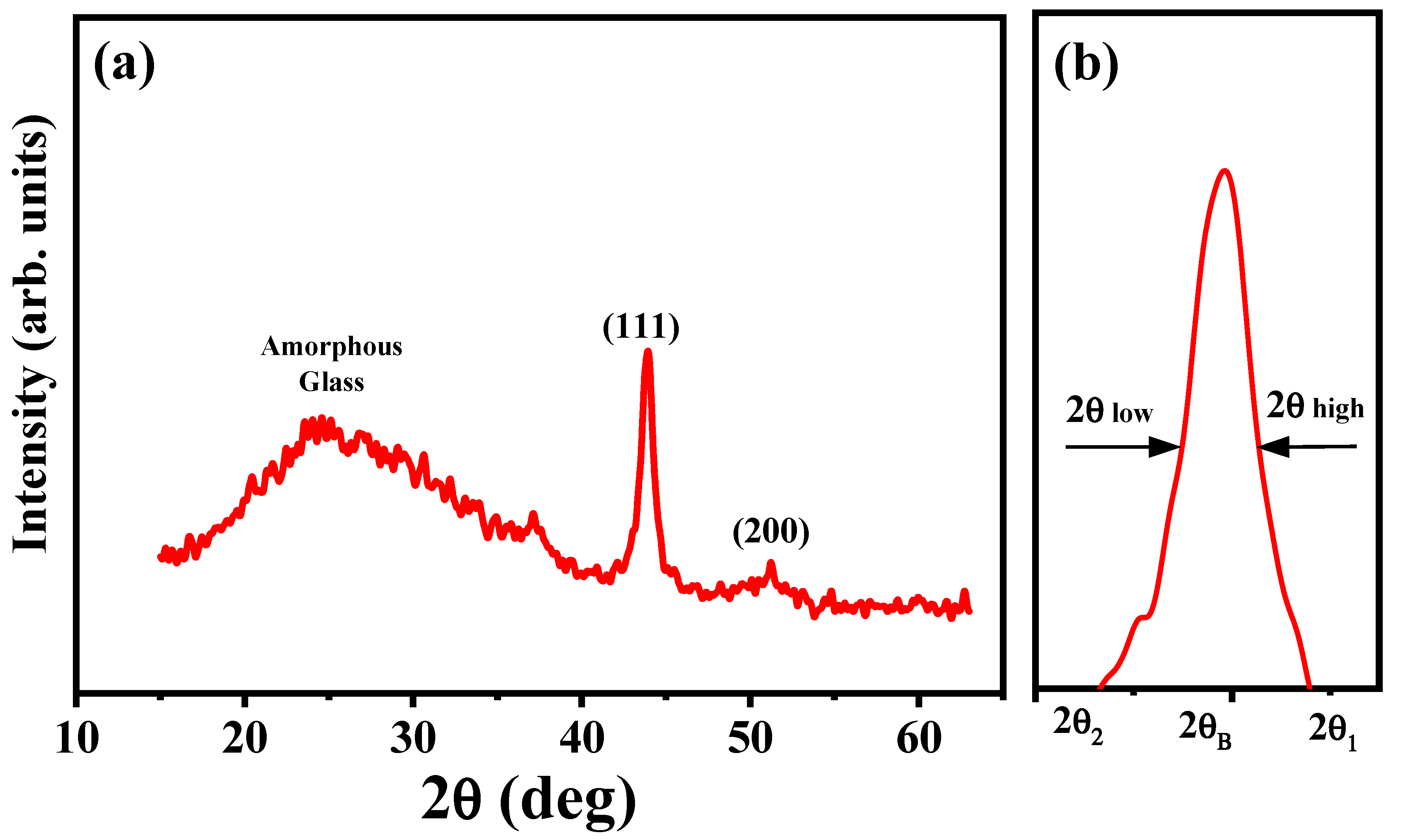
3. Results and Discussions
4. Conclusions
Author Contributions
Funding
Institutional Review Board Statement
Informed Consent Statement
Data Availability Statement
Acknowledgments
Conflicts of Interest
References
- Sivakumar, J.; Premkumar, C.; Santhanam, P.; Saraswathi, N. Biosynthesis of silver nanoparticles using Calotropis gigantean leaf. Afr. J. Basic Appl. Sci. 2011, 3, 265–270. [Google Scholar]
- Din, M.I.; Rehan, R. Synthesis, Characterization, and Applications of Copper Nanoparticles. Anal. Lett. 2017, 50, 50–62. [Google Scholar] [CrossRef]
- Hudlikar, M.; Joglekar, S.; Dhaygude, M.; Kodam, K. Latex-mediated synthesis of ZnS nanoparticles: Green synthesis approach. J. Nanoparticle Res. 2012, 14, 1–6. [Google Scholar] [CrossRef]
- Singh, R.P.; Shukla, V.K.; Yadav, R.S.; Sharma, P.K.; Singh, P.K.; Pandey, A.C. Biological approach of zinc oxide nanoparticles formation and its characterization. Adv. Mater. Lett. 2011, 2, 313–317. [Google Scholar] [CrossRef]
- Awwad, A.M.; Salem, N.M.; Abdeen, A.O. Biosynthesis of Silver Nanoparticles using Olea europaea Leaves Extract and its Antibacterial Activity. Nanosci. Nanotechnol. 2012, 2, 164–170. [Google Scholar] [CrossRef] [Green Version]
- Reed, M.A.; Randall, J.N.; Aggarwal, R.J.; Matyi, R.J.; Moore, T.M.; Wetsel, A.E. Observation of discrete electronic states in a zero-dimensional semiconductor nanostructure. Phys. Rev. Lett. 1988, 60, 535–537. [Google Scholar] [CrossRef]
- Takagahara, T. Effects of dielectric confinement and electron-hole exchange interaction on excitonic states in semiconductor quantum dots. Phys. Rev. B 1993, 47, 4569–4584. [Google Scholar] [CrossRef] [PubMed]
- Zheng, N.; Fan, J.; Stucky, G.D. One-Step One-Phase Synthesis of Monodisperse Noble-Metallic Nanoparticles and Their Colloidal Crystals. J. Am. Chem. Soc. 2006, 128, 6550–6551. [Google Scholar] [CrossRef]
- Easom, K.A.; Klabunde, K.J.; Sorensen, C.; Hadjipanayis, G.C. Nanoscale magnetic particles. New methods to surface protected metallic and immiscible bimetallic clusters/particles. Polyhedron 1994, 13, 1197–1223. [Google Scholar] [CrossRef]
- Wu, W.; Shen, J.; Banerjee, P.; Zhou, S. Core–shell hybrid nanogels for integration of optical temperature-sensing, targeted tumor cell imaging, and combined chemo-photothermal treatment. Biomaterials 2010, 31, 7555–7566. [Google Scholar] [CrossRef]
- Gawande, M.B.; Goswami, A.; Felpin, F.-X.; Asefa, T.; Huang, X.; Silva, R.; Zou, X.; Zboril, R.; Varma, R.S. Cu and Cu-Based Nanoparticles: Synthesis and Applications in Catalysis. Chem. Rev. 2016, 116, 3722–3811. [Google Scholar] [CrossRef] [Green Version]
- Wunder, S.; Polzer, F.; Lu, Y.; Mei, Y.; Ballauff, M. Kinetic Analysis of Catalytic Reduction of 4-Nitrophenol by Metallic Nanoparticles Immobilized in Spherical Polyelectrolyte Brushes. J. Phys. Chem. C 2010, 114, 8814–8820. [Google Scholar] [CrossRef]
- Homola, J.; Yee, S.S.; Gauglitz, G. Surface plasmon resonance sensors: Review. Sens. Actuators B Chem. 1999, 54, 3–15. [Google Scholar] [CrossRef]
- Taton, T.A.; Mirkin, C.A.; Letsinger, R.L. Scanometric DNA Array Detection with Nanoparticle Probes. Science 2000, 289, 1757–1760. [Google Scholar] [CrossRef] [Green Version]
- Sun, S.; Murray, C.B.; Weller, D.; Folks, L.; Moser, A. Monodisperse FePt Nanoparticles and Ferromagnetic FePt Nanocrystal Superlattices. Science 2000, 287, 1989–1992. [Google Scholar] [CrossRef]
- Glavee, G.N.; Klabunde, K.J.; Sorensen, C.; Hadjipanayis, G.C. Borohydride reduction of cobalt ions in water. Chemistry leading to nanoscale metal, boride, or borate particles. Langmuir 1993, 9, 162–169. [Google Scholar] [CrossRef]
- Liz-Marzán, L.M.; Touriño, I.L. Reduction and Stabilization of Silver Nanoparticles in Ethanol by Nonionic Surfactants. Langmuir 1996, 12, 3585–3589. [Google Scholar] [CrossRef]
- Yu, Y.Y.; Chang, S.-S.; Lee, C.-L.; Wang, C.R.C. Gold Nanorods: Electrochemical Synthesis and Optical Properties. J. Phys. Chem. B 1997, 101, 6661–6664. [Google Scholar] [CrossRef]
- Maksoud, M.I.A.A.; Fahim, R.A.; Shalan, A.E.; Elkodous, M.A.; Olojede, S.O.; Osman, A.I.; Farrell, C.; Al-Muhtaseb, A.H.; Awed, A.S.; Ashour, A.H.; et al. Advanced materials and technologies for supercapacitors used in energy conversion and storage: A review. Environ. Chem. Lett. 2021, 19, 375–439. [Google Scholar] [CrossRef]
- Sanad, M.F.; Shalan, A.E.; Abdellatif, S.O.; Abu Serea, E.S.; Adly, M.S.; Ahsan, A. Thermoelectric Energy Harvesters: A Review of Recent Developments in Materials and Devices for Different Potential Applications. Top. Curr. Chem. 2020, 378, 1–43. [Google Scholar] [CrossRef] [PubMed]
- Mallik, K.; Mandal, M.; Pradhan, A.N.; Pal, T. Seed Mediated Formation of Bimetallic Nanoparticles by UV Irradiation: A Photochemical Approach for the Preparation of “Core−Shell” Type Structures. Nano Lett. 2001, 1, 319–322. [Google Scholar] [CrossRef]
- Tolaymat, T.M.; El Badawy, A.M.; Genaidy, A.; Scheckel, K.; Luxton, T.P.; Suidan, M. An evidence-based environmental perspective of manufactured silver nanoparticle in syntheses and applications: A systematic review and critical appraisal of peer-reviewed scientific papers. Sci. Total. Environ. 2010, 408, 999–1006. [Google Scholar] [CrossRef] [Green Version]
- Somorjai, G.A.; Park, J.Y. Molecular Factors of Catalytic Selectivity. Angew. Chem. Int. Ed. 2008, 47, 9212–9228. [Google Scholar] [CrossRef] [PubMed]
- Ben Aissa, M.A.; Tremblay, B.; Andrieux-Ledier, A.; Maisonhaute, E.; Raouafi, N.; Courty, A. Copper nanoparticles of well-controlled size and shape: A new advance in synthesis and self-organization. Nanoscale 2015, 7, 3189–3195. [Google Scholar] [CrossRef] [Green Version]
- Smith, W.F. Principles of Materials Science and Engineering; Mc-Graw Hill Series: New York, NY, USA, 1999. [Google Scholar]
- Khan, A.; Rashid, A.; Younas, R.; Chong, R. A chemical reduction approach to the synthesis of copper nanoparticles. Int. Nano Lett. 2016, 6, 21–26. [Google Scholar] [CrossRef] [Green Version]
- Murugadoss, G.; Rajamannan, B.; Madhusudhanan, U. Synthesis and characterization of water-soluble ZnS: Mn2+ nanocrystals. Chalcogenide Lett. 2009, 6, 197–201. [Google Scholar]
- Hussain, M.A.; Choi, E.J.; Maqbool, A.; Atif, M.; Zeb, H.; Yeo, J.; Yu, J.-A.; Cho, Y.-H.; Noh, M.; Kim, J.W. An efficient hydration of nitriles with ruthenium-supported heterogeneous catalyst in water under moderate conditions. J. Ind. Eng. Chem. 2021, 99, 187–195. [Google Scholar] [CrossRef]
- Maqbool, A.; Hussain, M.A.; Khalid, F.A.; Bakhsh, N.; Hussain, A.; Kim, M.H. Mechanical characterization of copper coated carbon nanotubes reinforced aluminum matrix composites. Mater. Charact. 2013, 86, 39–48. [Google Scholar] [CrossRef]
- Karimov, K.S.; Khalid, F.A.; Chani, M.; Mateen, A.; Hussain, M.A.; Maqbool, A.; Ahn, J. Carbon nanotubes based flexible temperature sensors. Optoelectron. Adv. Mater. Rapid Commun. 2012, 6, 194–196. [Google Scholar]
- Karimov, K.S.; Chani, M.T.S.; Khalid, F.A. Carbon nanotubes film based temperature sensors. Phys. E Low Dimens. Syst. Nanostructures 2011, 43, 1701–1703. [Google Scholar] [CrossRef]


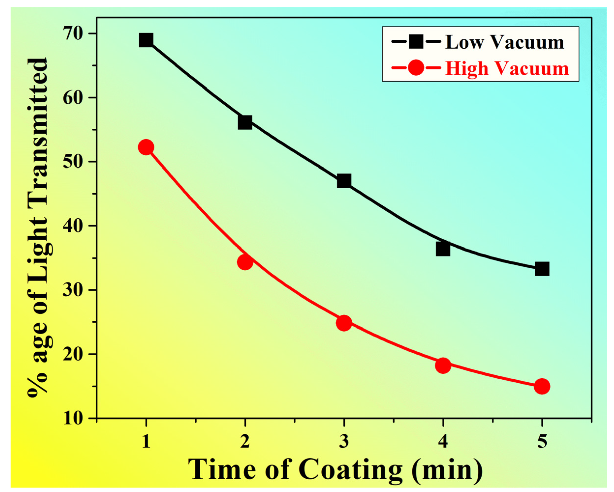
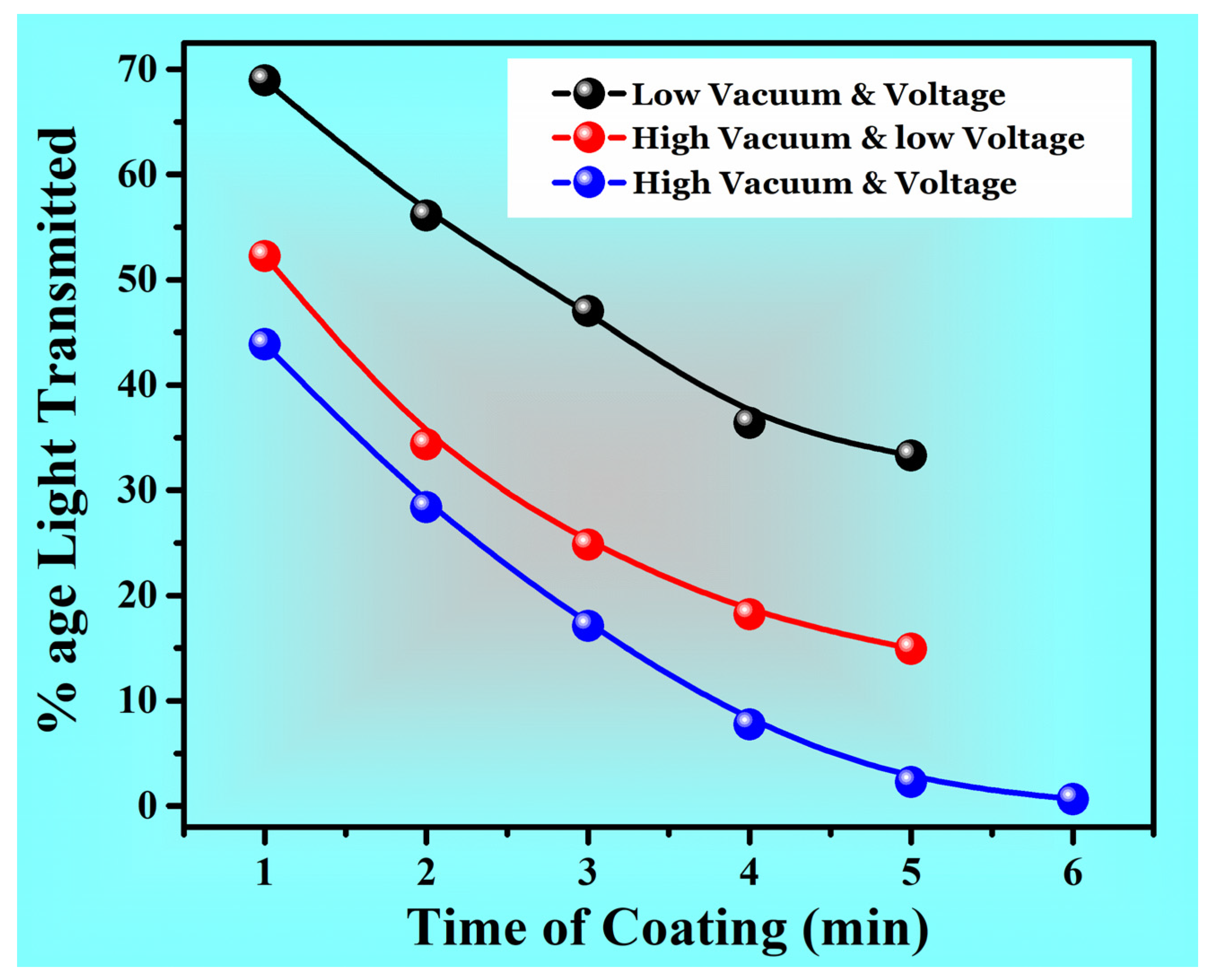
| Category No. | Pressure during Coating “torr” | Voltage “K-Volt” | Current “mA” |
|---|---|---|---|
| 1 | 2 | 0.9 | 25 |
| 2 | 10−1 | 0.9 | 25 |
| 3 | 10−1 | 1.45 | 13 |
| Coating Time “min” | 1 | 2 | 3 | 4 | 5 | |
|---|---|---|---|---|---|---|
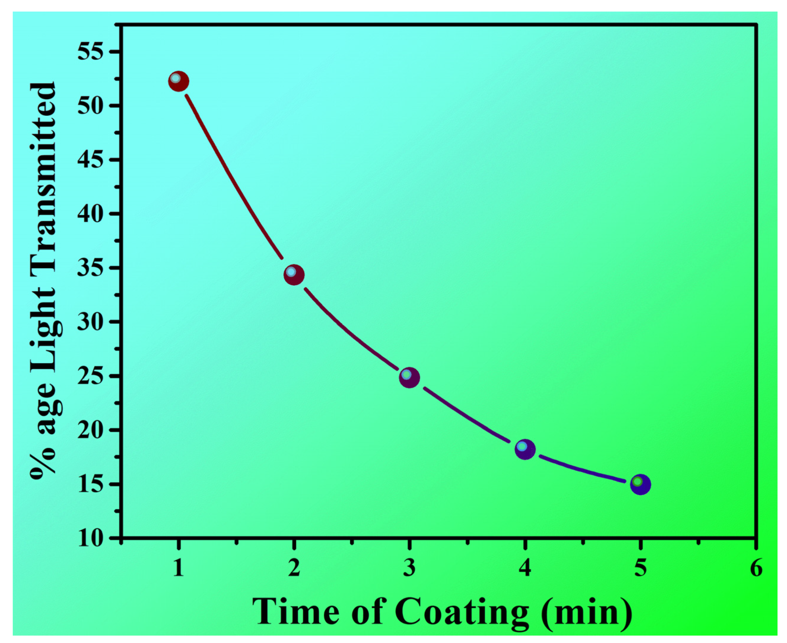
| Percentage Light Intensity Transmitted | Category 1 | 68.93 | 56.1 | 52.27 | 36.4 | 33.3 |
| Category 2 | 52.24 | 34.33 | 31.34 | 18.18 | 14.93 | |
| Category 3 | 43.87 | 28.39 | 17.1 | 7.74 | 2.26 | |
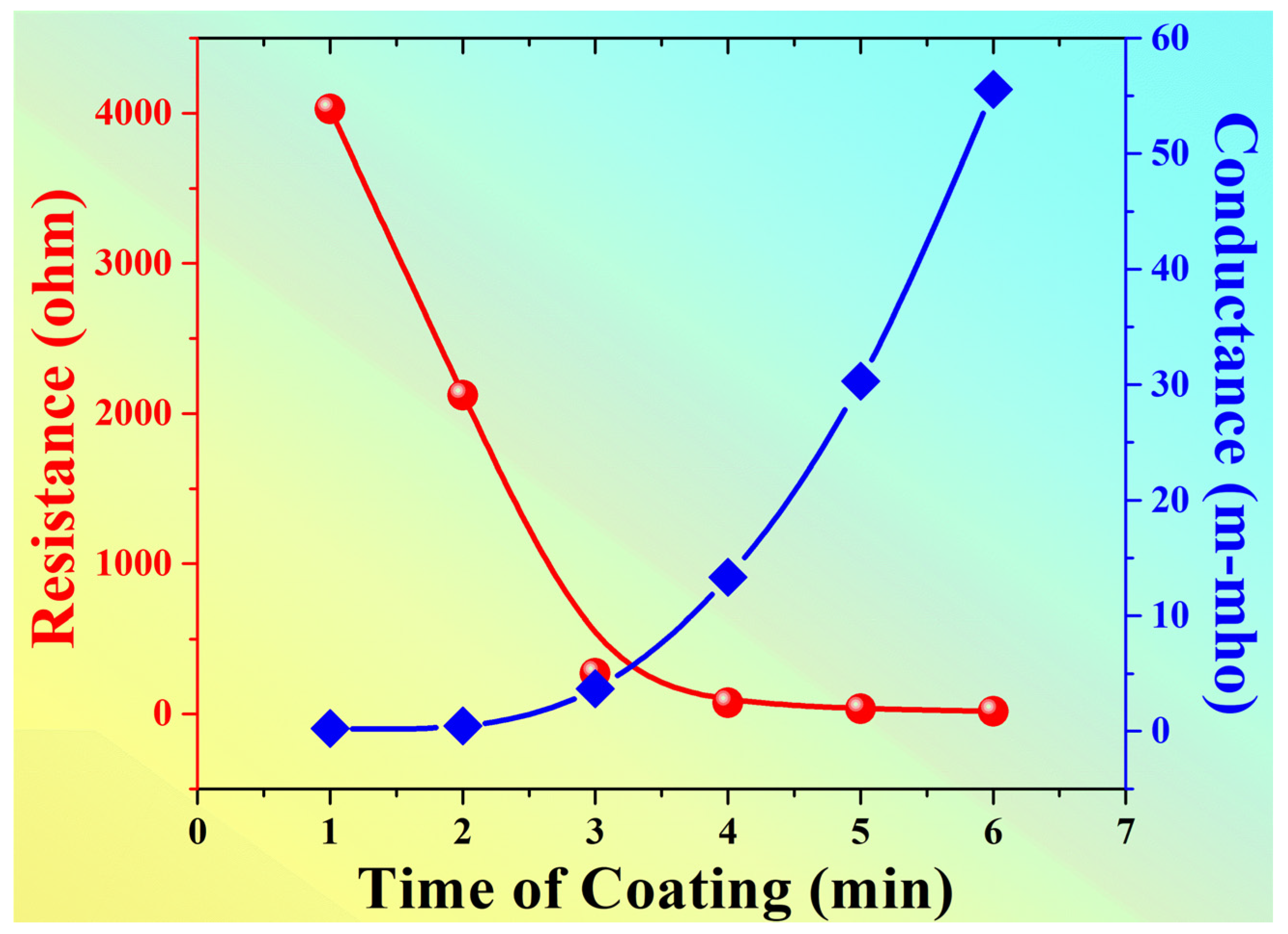
| Time of Coating “min” | 1 | 2 | 3 | 4 | 5 |
|---|---|---|---|---|---|
| Voltage “volt” | 40.26 | 21.23 | 2.71 | 0.75 | 0.33 |
| Resistance “Ω” | 4026 | 2123 | 271 | 75 | 33 |
| Conductance “m-mho” | 0.248 | 0.471 | 3.69 | 13.33 | 30.30 |
| Sr. No. | Average Thickness “nm” | Average Roughness “nm” | Maximum Island Thickness “nm” |
|---|---|---|---|
| Area 1 | 19.8 | 4.3 | 36.6 |
| Area 2 | 20.7 | 4.5 | 50.1 |
Publisher’s Note: MDPI stays neutral with regard to jurisdictional claims in published maps and institutional affiliations. |
© 2022 by the authors. Licensee MDPI, Basel, Switzerland. This article is an open access article distributed under the terms and conditions of the Creative Commons Attribution (CC BY) license (https://creativecommons.org/licenses/by/4.0/).
Share and Cite
Alrobei, H.; Maqbool, A.; Hussain, M.A.; Malik, R.A.; Karim, M.R.A.; AlBaijan, I.; Hafiz, A.; Latif, M. Single-Step Fabrication and Characterization of Nanoscale Cu Thinfilms for Optoelectronic Applications. Crystals 2022, 12, 62. https://doi.org/10.3390/cryst12010062
Alrobei H, Maqbool A, Hussain MA, Malik RA, Karim MRA, AlBaijan I, Hafiz A, Latif M. Single-Step Fabrication and Characterization of Nanoscale Cu Thinfilms for Optoelectronic Applications. Crystals. 2022; 12(1):62. https://doi.org/10.3390/cryst12010062
Chicago/Turabian StyleAlrobei, Hussein, Adnan Maqbool, Muhammad Asif Hussain, Rizwan Ahmed Malik, Muhammad Ramzan Abdul Karim, Ibrahim AlBaijan, Azeem Hafiz, and Muhammad Latif. 2022. "Single-Step Fabrication and Characterization of Nanoscale Cu Thinfilms for Optoelectronic Applications" Crystals 12, no. 1: 62. https://doi.org/10.3390/cryst12010062
APA StyleAlrobei, H., Maqbool, A., Hussain, M. A., Malik, R. A., Karim, M. R. A., AlBaijan, I., Hafiz, A., & Latif, M. (2022). Single-Step Fabrication and Characterization of Nanoscale Cu Thinfilms for Optoelectronic Applications. Crystals, 12(1), 62. https://doi.org/10.3390/cryst12010062