Communication

Dynamic Performance Characterization Techniques in Gallium Nitride-Based Electronic Devices

Department of Information Engineering, University of Padova, 35131 Padova, Italy
*
Author to whom correspondence should be addressed.
Crystals 2021, 11(9), 1037; https://doi.org/10.3390/cryst11091037
Submission received: 19 July 2021 / Revised: 24 August 2021 / Accepted: 25 August 2021 / Published: 28 August 2021

Abstract

:
In this paper, we compare and discuss the main techniques for the analysis of the dynamic performance of GaN-based transistors. The pulsed current-voltage characterization provides information on the effect of different trapping voltages on various bias points of the device under test, leading to the detection of all the possible effects, as well as to the choice of the optimal filling and measure bias conditions in other techniques. The drain current transients use one of the identified bias configurations to extract information on the deep level signature responsible for the performance variation and, thus, they can pinpoint the corresponding physical crystal lattice configuration, providing useful information to the growers on how the issue can be solved. Finally, given the complex interplay between the filling and emission time constants, the gate frequency sweeps can be used to obtain the real performance in the target operating condition.

1. Introduction

Gallium nitride transistors have recently emerged as excellent devices for application in power electronics. The high breakdown field of GaN (3.3 MV/cm), the high conductivity of the 2-dimensional electron gas, and the wide bandgap of GaN and AlGaN enable high voltage (kV range) applications, high temperature operation, and low on-resistance. Despite the important efforts carried out by researchers in the field, there are still open questions and issues concerning the physics of such devices.
More specifically, a number of physical mechanisms still limit the dynamic performance of the transistors. This paper describes the most common techniques for analyzing the dynamic performance of GaN transistors.

2. The Arrhenius Law

Gallium nitride is typically grown on foreign substrates (hetero-epitaxial growth) due to the high cost and low availability of native substrates. The lattice and thermal mismatch between GaN and substrate causes a high number of deviations of the crystal structure from ideality, globally referred to as “defects”. These defects add unwanted allowed energy states inside the forbidden bandgap, whose energetic configuration roughly resembles a potential well. Carriers of any polarity may get trapped inside these locations, effectively changing the local potential profile and influencing other carriers due to their electrical charge and electrostatic interaction. When the defect density is high, a significant number of carriers may be trapped, leading to a strong variation in the device performance compared to the ideal one.
The environment close to the defect has a significant impact on the average time for the emission of the trapped charge, mostly due to the effect of temperature, which promotes de-trapping via multi-phonon absorption, and of the electric field, that enhances tunneling and lowers potential barriers due to the Poole-Frenkel effect. Additionally, most deep levels have barriers not only for the emission but also for the capture of carriers, and extended defects generally behave as mini-bands of deep levels, leading to strong deviations from the ideal trap behavior. All these effects are non-linear and make the derivation of a comprehensive theoretical model more complex. For this reason, the de-trapping kinetics of deep levels in semiconductors are usually described according to the Arrhenius law, which after grouping physical constants and the temperature dependence takes the form:
e n = σ n γ n T 2 e E a k B T
where e n is the emission rate, σ n the apparent cross-section, γ n a material-dependent constant, T the temperature, E a the activation energy ( E C E T for electron traps and E T E V for hole traps, where E T is the energy of the deep level) and k B the Boltzmann constant. Therefore, in a plot of ln ( T 2 / e n ) vs q / k B T (the so-called Arrhenius plot), the data points originating from different emission rates (one for each temperature) are placed in a straight line, whose slope is the activation energy. The apparent cross section can be computed from the intercept of the linear fit.
The activation energy and apparent cross section are the most important parameters summarizing the behavior of the deep level under analysis. With the aim of finding information on the possible physical origin, they can be used to compare with the literature the data obtained thanks to several characterization techniques.

3. Methodologies for Studying Charge Trapping in GaN Transistors

All the indirect deep level characterization techniques have different approaches but are based on the same idea: Monitoring the variation over time of one electrical parameter sensitive to the trapping level of the device after an external stimulus is applied to change the trap occupancy state. The external stimulus may be electrical, i.e., a variation in the bias, or optical, in the optical deep level transient spectroscopy (O-DLTS) [1], deep level optical spectroscopy (DLOS) [2] or photocurrent spectroscopy (PCS) [3]. The measured parameter, in the case of devices with a depletion region, may be the capacitance, such as in the capacitance deep level transient spectroscopy (C-DLTS) [4], or the conductance, in the thermal admittance spectroscopy (TAS) [5,6]. The requirement of a depletion region for these techniques implies that their use is possible only on the gate stack, limiting their usefulness and ease of operation on transistors with respect to simple diodes; and thereby leading to other preferred techniques. Measuring the current flowing in the channel as trapping sensitive parameter is easier, and therefore current-based techniques, such as the current deep level transient spectroscopy (I-DLTS) [7,8] are more popular. Given that a complete description of all the possible techniques would be too long and complex, in the remaining part of this section we will present only three additional current-based techniques, which have the widest field of application. The reader interested in further information on the aforementioned techniques may read the corresponding references.

3.1. Pulsed Current-Voltage Characterization

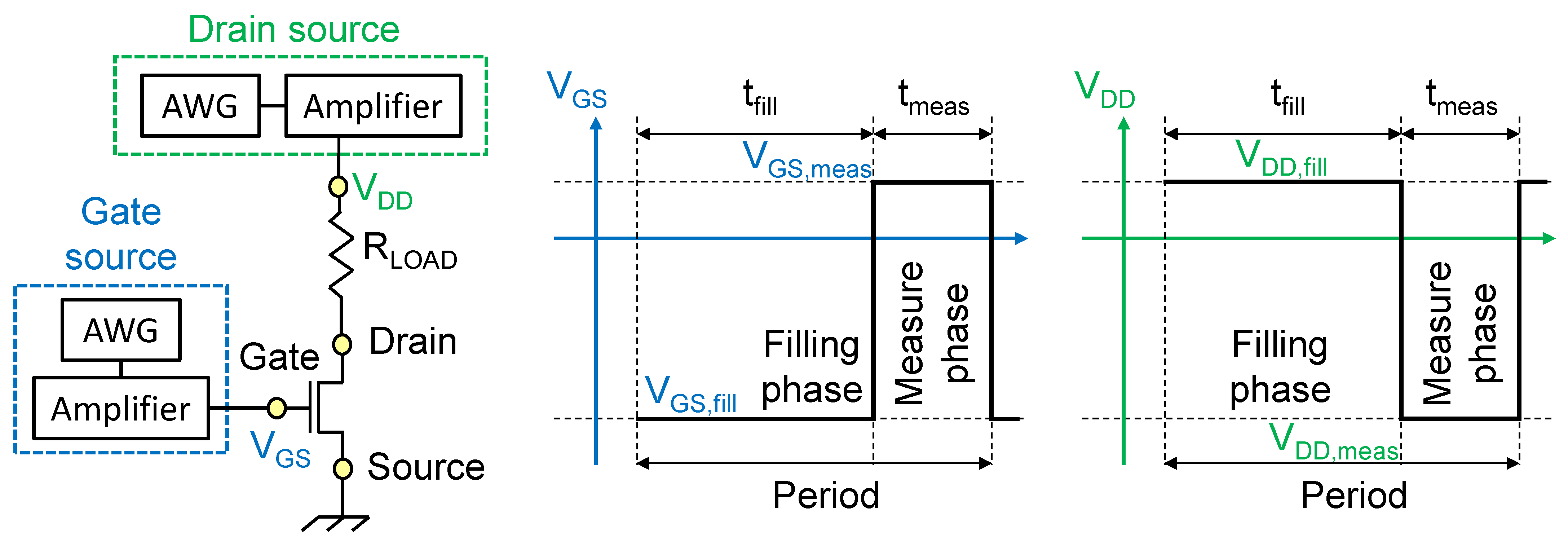
The pulsed current-voltage characterization (PIV), also known as double pulse (DP), is a combination of the gate-lag and drain-lag techniques. In this case, the trapping sensitive parameter is the drain current, measured as the voltage drop over a known resistance by means of a voltage probe (see Figure 1). The gate voltage source and drain voltage source can be obtained by several approaches, such as by designing a dedicated circuit or by using commercially-available pulsers and/or arbitrary waveform generators (AWG) coupled with amplifiers. This voltage source configuration is highly flexible in both timings and voltages. Therefore, the same schematic can be used to carry out all the other techniques presented in this paper.
The voltage profile of the single measured point is shown in Figure 1. The first part is the filling phase: the device is kept at a constant V G S , f i l l and V D D , f i l l voltage (usually called quiescent bias voltage) for a t f i l l time (for instance 99 μs) in order to promote the trapping. The device bias is then rapidly changed by means of a voltage pulse ( t m e a s long, usually 1 μs) applied both at the gate and at the drain side in order to carry out the measurement at the desired V G S , m e a s and V D D , m e a s voltage, leading to the detection of the effect of the trapping. This single measurement routine is then repeated several times at different measure voltages, allowing for the reconstruction of the whole dynamic I D V D and I D V G curve, thereby, detecting the impact of the quiescent bias point on the ON-resistance, saturation current, threshold voltage and transconductance value.
The various deep levels may theoretically be located in any position inside the device, including surface and interfaces, the barrier layer, the buffer layer and the gate insulator or p-type gate layer, if present. A first-order distinction between traps located in different parts of the devices may be provided by keeping in mind that the driving forces of the trapping are the electric field and the flow of current. Therefore, by choosing appropriate bias levels for the filling and measure phase it is possible to selectively excite the trapping in specific regions, allowing at least the distinction of effects originating from the source and drain access region or from the gate stack. In the former case, it is necessary to provide an electric field or current flow in the lateral source to drain direction, i.e., to vary the voltage applied at the drain, while keeping the source, gate and bulk bias constant. In the latter case, the driving force needs to be applied in the vertical gate to bulk direction, i.e., the gate or bulk potential should be changed without any variation at the source or drain terminals.

3.2. Drain Current Transients

The drain current transient (DCT) measurements are a powerful technique that can complement the double pulse, providing information on the activation energy and on the apparent cross-section of the deep levels [9,10]. The experimental setup is the same used in the double pulse: monitoring the variation in the drain current, as the voltage drop over a known resistance, induced by a given trapping voltage at the measurement bias voltage of interest. There are several differences between the two techniques. The duration of the filling is significantly longer, typically up to 100 s, in order to ensure the complete filling of all the deep levels. The measurement phase is longer too, again up to 100 s, and the whole current vs time waveform is recorded, beginning from the shortest time interval allowed by the experimental setup, usually in the range from 1 μs to 10 μs. Therefore, due to the length of the single measurement point, often only few measure voltages are recorded. These recorded voltages are typically one in the linear region, to investigate the effect of the trapping on the ON-resistance, and one in the saturation region, to analyze the effect on the threshold voltage. The last difference is the fact that the measurement is repeated at various temperatures, in order to analyze the effect of the temperature on the capture and emission processes.
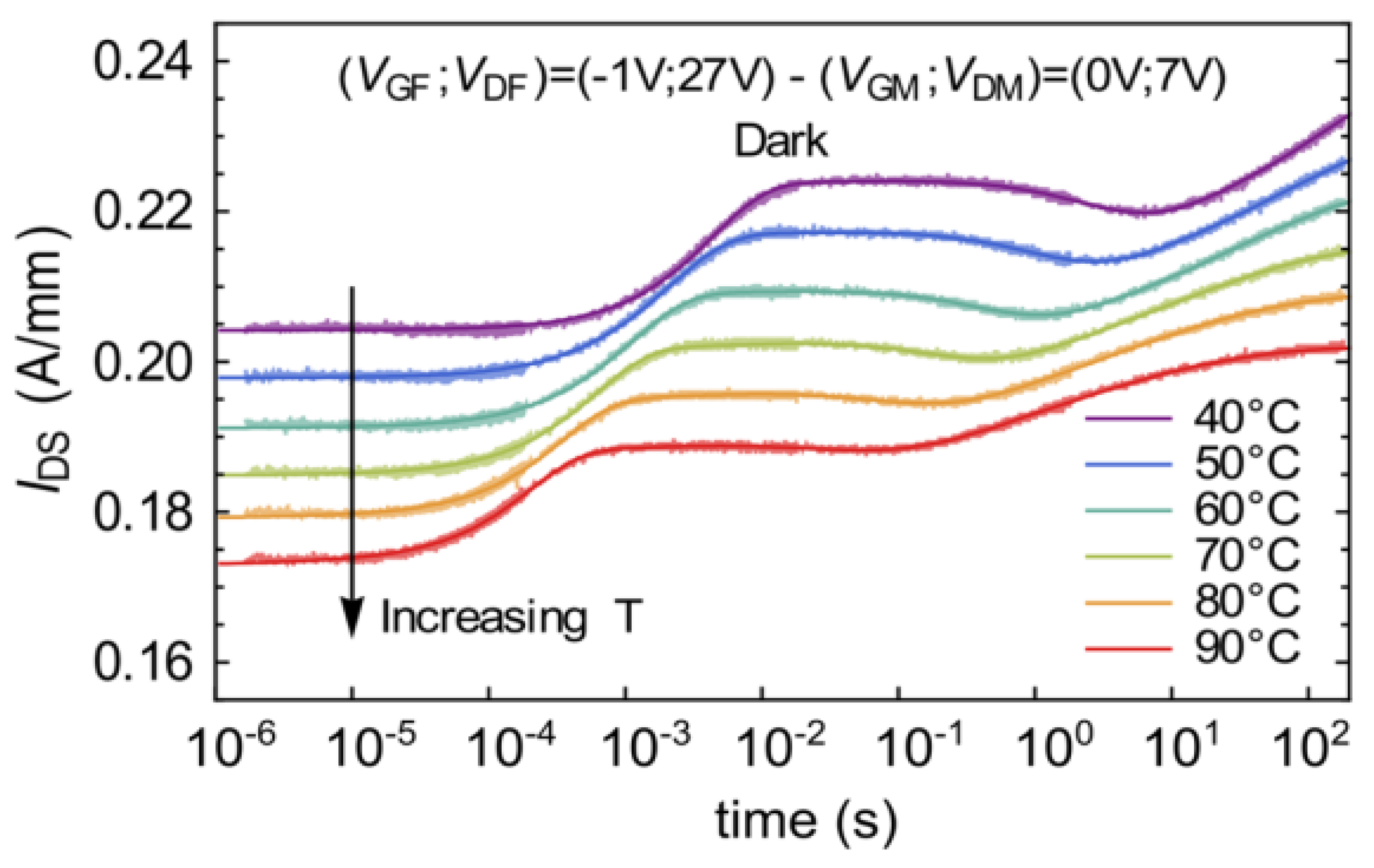
A typical drain current transient measurement is shown in Figure 2: in semi-logarithmic x scale, each exponential emission or capture process appears as an edge connecting two different steady-state values, and the position of the edge gives an indication on the characteristic time constant τ of the emission from the deep level at that temperature. By changing the temperature, the time constant moves to faster values and its value can be used to construct the Arrhenius plot of the deep level. The reason why this technique is so powerful compared to other approaches is its experimental ease: by means of few measurements carried out close to room temperature, it is possible to extrapolate information on several deep levels, thanks to the wide time scale investigated. Additional details on the samples under test, the extrapolated traps, their origin and effects can be found in ref. [9].
Although the experimental setup is not intricate, a high level of complexity is present in the extrapolation of the time constant at the measurement temperature from the current transient. At least three different techniques can be used.
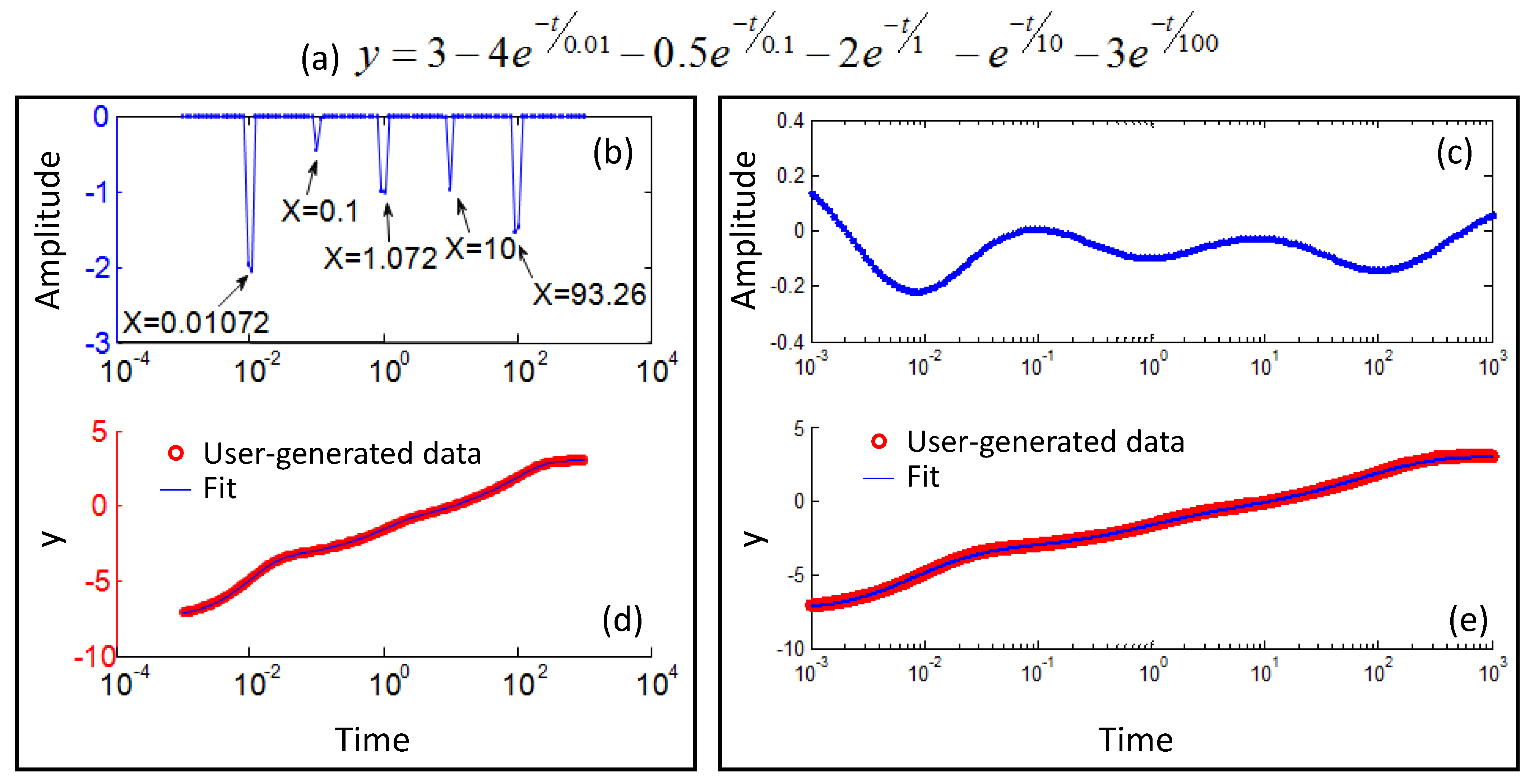
The first method is called the multi-exponential fit. In this case, the user defines a custom fitting function, composed of the sum of several exponential functions with a fixed time constant. The higher the number of exponentials the better the extrapolation of the time constant due to the higher resolution, but also the heavier the computational load. Additionally, in this case, the proper design of the fitting algorithm is critical in order to reach the best level of accuracy and to ensure the correct analysis of the experimental data. As can be seen in Figure 3, when a highly complex user-generated transient is analyzed (equation (a)), this method may lead to very broad peaks and to (c) an inaccurate reconstruction of the various time constants and amplitudes of each transient component even though (e) the corresponding fitting quality may seem good. Conversely, an appropriate design of the algorithm leads to (b) the perfect extrapolation of both the time constant and the trap amplitude even in the case of closely-spaced or very weak trap responses, and (d) to the perfect reconstruction of the source transient.
The second method takes into account the specific properties of extended defects and uses, instead of simple exponential, the more accurate stretched exponential description
I ( t ) = I 0 + I 1 e ( t τ ) β
The additional stretching parameter β (0 < β < 1) increases the fitting complexity, making a multi-exponential approach not possible due to the higher computational load and more importantly, to issues reaching the convergence of the fit process. For this reason, the fit cannot be carried out automatically, and every sub-section of the transient has to be manually evaluated, lowering the overall accuracy of the method in the case of non-stretched exponential.
The third method originates from the consideration that, in semi-logarithmic x scale, an exponential variation appears as an edge. The first step of this method is to post-process the experimental data by means of a high-order polynomial fit, typically up to the 11th order, in order to filter out the noise. The derivative of the resulting fit is then computed, in order to detect the edges corresponding to every capture and emission process as peaks in the time constant spectrum.
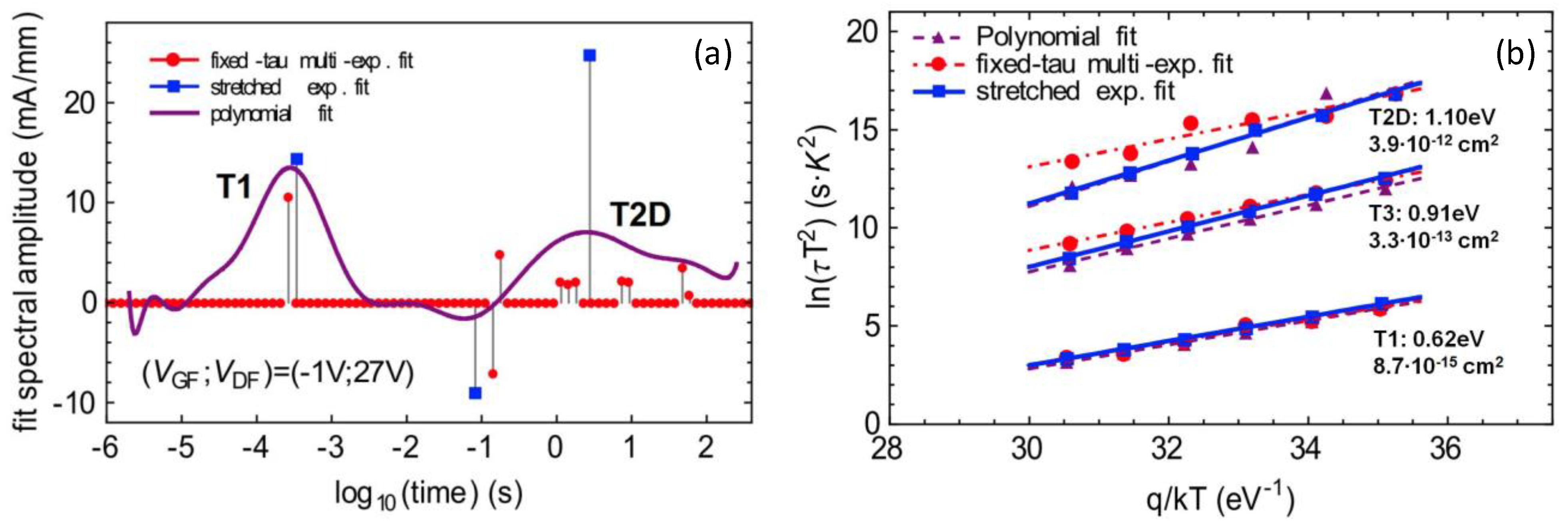
Figure 4 compares the time constant spectra and Arrhenius plots extrapolated by using the three methods on the data of Figure 2, including a non-stretched and an extended defect. As can be observed, the stretched exponential fit yields good results, but is not able to reconstruct a non-stretched exponential, as well as the multi-exponential fit. Conversely, the multi-exponential fit yields the best accuracy, but it is a slow method. A plus is the fact that it decomposes a stretched exponential in the sum of several exponential (see abscissa from 0 to 2 in Figure 4a), and thus, points out the correct regions where the stretched exponential fit has to be carried out. The polynomial fit is the least accurate method and does not provide any information on the absolute trap amplitude, but it is the fastest method to implement and perform, and yields Arrhenius signatures compatible with the two other methods (see Figure 4b).
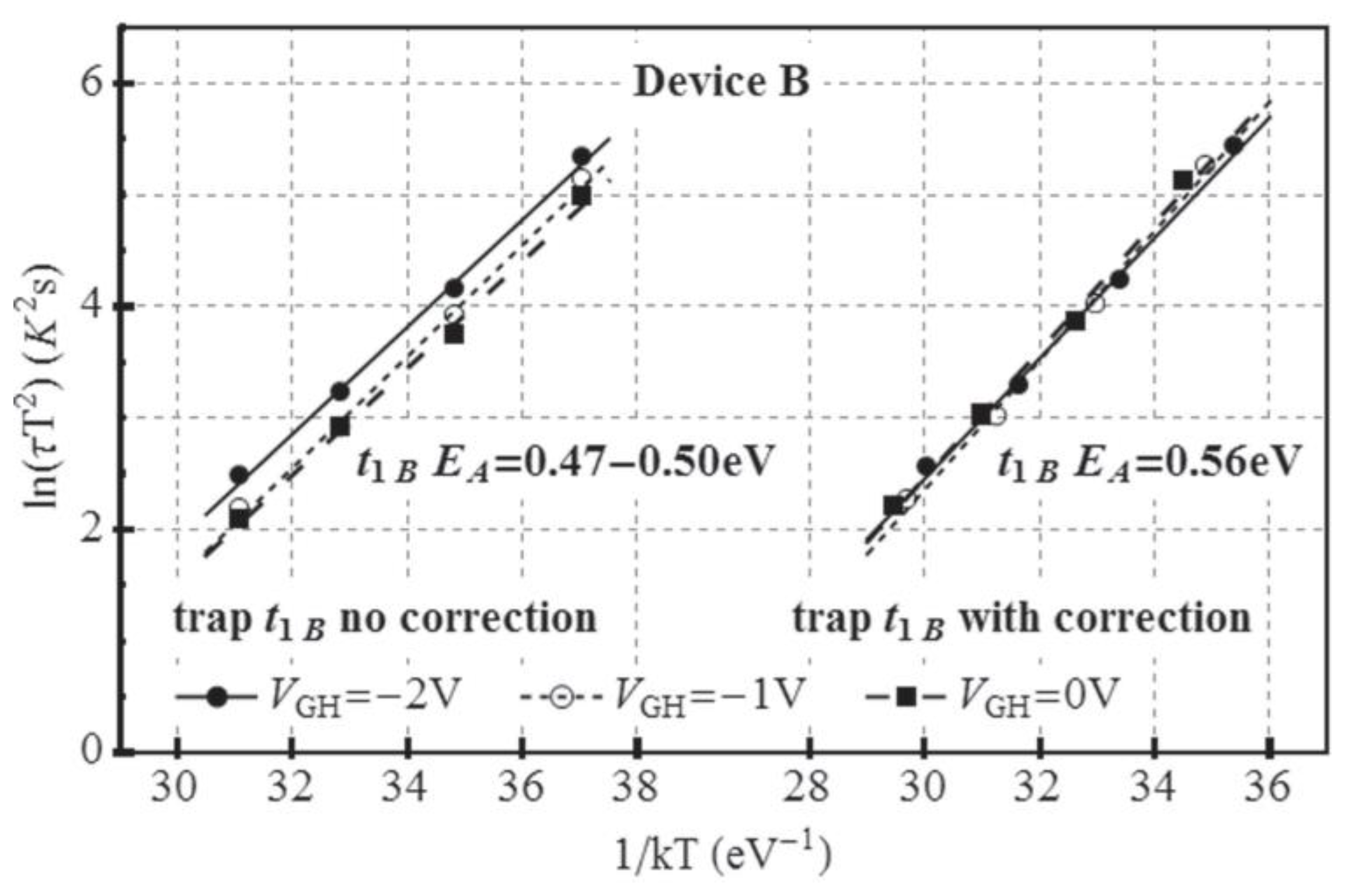
The last point that has to be taken into account is the self-heating of the device during the measurement phase. The short t m e a s of the double pulse measurement yields a negligible effect, that becomes more and more important during the long measure time of the drain current transient measurement. For this reason, the effective temperature T e f f to be used in the Arrhenius plot is not the external temperature setpoint T e x t , but has to be increased by taking into account the thermal resistance R t h of the device and the dissipated power P d i s s according to:
T e f f = T e x t + R t h P d i s s
The temperature correction leads to different activation energy and apparent cross-section values, and uniforms data taken at different dissipated power levels, as described in [11] (see Figure 5).

3.3. Gate Frequency Sweeps

The current values of a device and its dynamic performance is a consequence of the superposition of all the trapping and de-trapping mechanisms that affect it. Since the time constant and the activation energy of every process are different, the actual time spent in off- and on-state by the device have a strong impact. In the final switching circuit, those two times are designed in terms of operating frequency, i.e., the reciprocal of the sum between the off- and on-state time, called period, and of duty cycle, i.e., the ratio between the on-state time and the period.
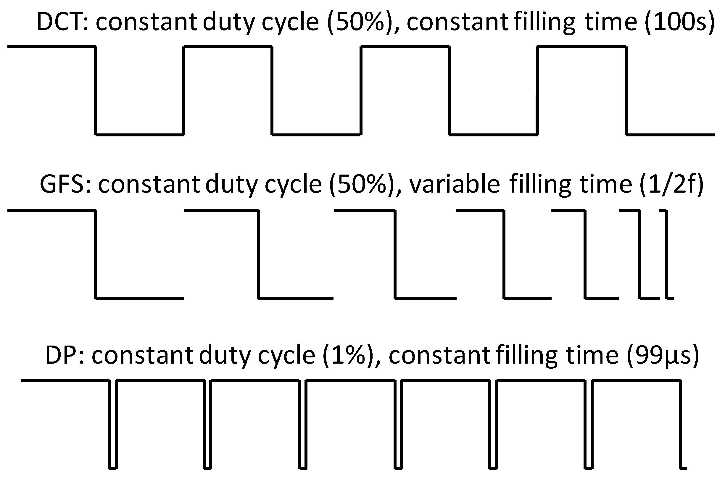
The effect of these two parameters cannot be readily evaluated by means of the two common techniques for the analysis of the trapping effects, namely the pulsed IV (PIV) and the drain current transients (DCT). An additional measurement technique that addresses this issue is the gate frequency sweep (GFS) [12]. The three techniques are compared in Figure 6. In the double pulse technique, a constant filling time (in the present case 99 μs) is used to fill the deep levels, and a very short measurement pulse (constant 1% duty cycle) is applied to the device under test, in order to monitor the effect of the trapping on the dynamic behavior of the output characteristics of the transistor, different from the one used in the final application. The drain current transients are based on a constant duty cycle, typically equal to the one of the real operation of the device (50% in the present case), but they use a very long filling time (usually in the range of few up to hundreds of seconds) in order to completely fill of the traps, leading to a completely unrealistic representation of the target operating frequency of the circuit. In the gate frequency sweep, the duty cycle is kept constant and equal to the designed value for the target application, and the filling time is varied continuously in order to track the effect of the operating frequency on the device under test.
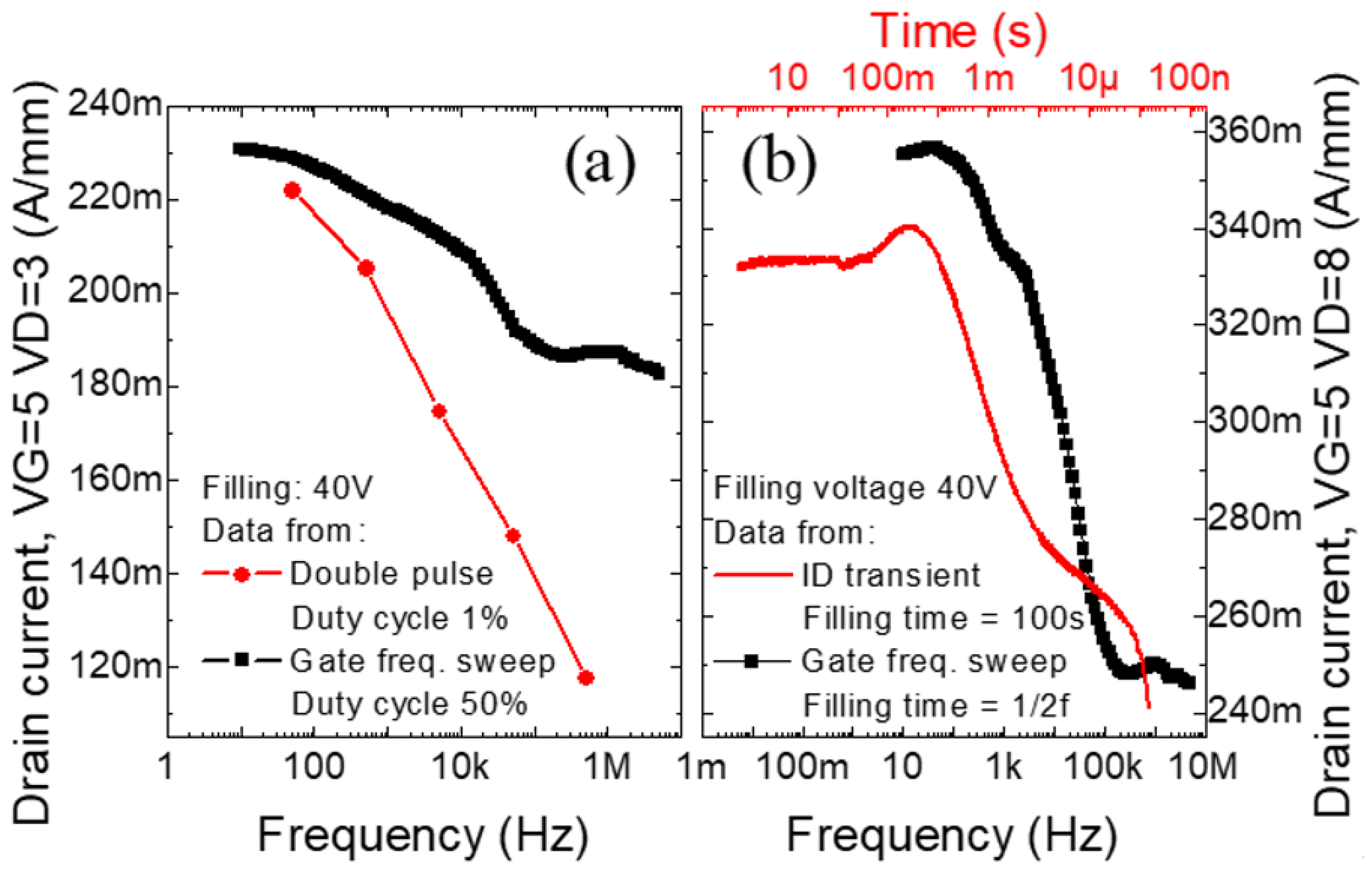
In the representative case of the device analyzed in [12], the three techniques were compared in compatible time ranges and lead to completely different results. As shown in Figure 7a, the double pulse leads to a severe overestimation of the effect of the off-state trapping, due to the very low duty cycle and therefore to an unrepresentative ratio between the duration of the trapping and de-trapping phase. Figure 7b compares the results of the DCT and GFS techniques. Even the drain current transients lead to the underestimation of the dynamic performance of the device under test, due to the constant and long filling time leading to more off-state trapping than the one that can be expected in the real operating conditions. Additionally, the drain current transient system is usually affected by a lower bandwidth.
It is important to point out that, since each technological choice and design parameter leads to a different deep level concentration inside the final device, the results reported in Figure 7 may significantly differ in other structures, and even if representative, cannot be generalized. Every device technology and iteration of the technological process have to be separately measured, in order to obtain a representative description of the trapping effects in the final application.

4. Conclusions

In summary, this paper focuses on the various characterization techniques that can be used to obtain information on the dynamic performance of gallium nitride-based devices. Each single technique has a different goal: identification of the relevant filling and trapping-affected bias points for the pulsed IV, identification of the deep level signature and its physical configuration for the drain current transients, identification of the real operating performance for the gate frequency sweeps. The three techniques must be used together to obtain all the information which is relevant for the full understanding of the trapping and detrapping processes in the device under test.

Author Contributions

All authors contributed equally to this work. All authors have read and agreed to the published version of the manuscript.

Funding

Part of this work was supported by MIUR (Italian Minister for Education) under the initiative "Departments of Excellence" (Law 232/2016). Work partially supported by Italian MIUR PRIN project GANAPP, and by the Office of Naval Research award N00014-20-1-2177, under the supervision of Paul Maki.

Data Availability Statement

The data presented in this study are available upon reasonable request to the corresponding author.

Conflicts of Interest

The authors declare no conflict of interest.

References

  1. Hamilton, B.; Peaker, A.R. Deep-state-controlled minority-carrier lifetime in n-type gallium phosphide. J. Appl. Phys. 1979, 50, 6373–6385. [Google Scholar] [CrossRef]
  2. Chantre, A.; Vincent, G.; Bois, D. Deep-level optical spectroscopy in GaAs. Phys. Rev. B 1981, 23, 5335–5359. [Google Scholar] [CrossRef]
  3. Tomm, J.W.; Bärwolff, A.; Jaeger, A.; Elsaesser, T. Deep level spectroscopy of high-power laser diode arrays. J. Appl. Phys. 1998, 84, 1325. [Google Scholar] [CrossRef]
  4. Lang, D.V. Deep-level transient spectroscopy: A new method to characterize traps in semiconductors. J. Appl. Phys. 1974, 45, 3023–3032. [Google Scholar] [CrossRef]
  5. Losee, D.L. Admittance spectroscopy of impurity levels in Schottky barriers. J. Appl. Phys. 1975, 46, 2204. [Google Scholar] [CrossRef]
  6. Barbolla, J.; Dueñas, S.; Bailón, L. Admittance spectroscopy in junctions. Solid-State Electron. 1992, 35, 285–297. [Google Scholar] [CrossRef]
  7. Borsuk, J.A.; Swanson, R.M. Current transient spectroscopy: A high-sensitivity DLTS system. IEEE Trans. Electron Devices 1980, 27, 2217–2225. [Google Scholar] [CrossRef]
  8. Li, Z. Systematic modelling and comparisons of capacitance and current-based microscopic defect analysis techniques for measurements of high-resistivity silicon detectors after irradiation. Nucl. Instrum. Methods Phys. Res. Sect. A Accel. Spectrom. Detect. Assoc. Equip. 1998, 403, 399–416. [Google Scholar] [CrossRef]
  9. Bisi, D.; Meneghini, M.; de Santi, C.; Chini, A.; Dammann, M.; Brückner, P.; Mikulla, M.; Meneghesso, G.; Zanoni, E. Deep-level characterization in GaN HEMTs-Part I: Advantages and limitations of drain current transient measurements. IEEE Trans. Electron Devices 2013, 60, 3166–3175. [Google Scholar] [CrossRef]
  10. Joh, J.; del Alamo, J.A. A Current-Transient Methodology for Trap Analysis for GaN High Electron Mobility Transistors. IEEE Trans. Electron Devices 2011, 58, 132–140. [Google Scholar] [CrossRef] [Green Version]
  11. Chini, A.; Soci, F.; Meneghini, M.; Meneghesso, G.; Zanoni, E. Deep levels characterization in GaN HEMTs—Part II: Experimental and numerical evaluation of self-heating effects on the extraction of traps activation energy. IEEE Trans. Electron Devices 2013, 60, 3176–3182. [Google Scholar] [CrossRef]
  12. De Santi, C.; Meneghini, M.; Ishida, H.; Ueda, T.; Meneghesso, G.; Zanoni, E. Gate frequency sweep: An effective method to evaluate the dynamic performance of AlGaN/GaN power heterojunction field effect transistors. Appl. Phys. Lett. 2014, 105, 073507. [Google Scholar] [CrossRef]
Figure 1. Schematic configuration and bias profiles of the pulsed current-voltage (or double pulse) measurement. The same circuital configuration can be used for all the other techniques presented in this paper.
Crystals 11 01037 g001
Figure 2. Typical drain current transient waveforms recorded at different temperatures.
Crystals 11 01037 g002
Figure 3. Reconstruction of a user-generated current transient according to equation (a) by using an optimized (b) and un-optimized (c) multi-exponential fit algorithm. even though both can visually reproduce the transient, (d) and (e) respectively, only the optimized algorithm can correctly reconstruct the time constants in the starting equation.
Crystals 11 01037 g003
Figure 4. (a) time constant spectra and (b) corresponding Arrhenius plots obtained on the data of Figure 2 by means of three different time constant extrapolation methods: the multi-exponential fit, the stretched exponential fit and the polynomial fit. © 2013 IEEE. Reprinted, with permission, from D. Bisi et al., “Deep-level Characterization in GaN HEMTs-Part I: Advantages and Limitations of Drain Current Transient Measurements,” in IEEE Transactions on Electron Devices, vol. 60, no. 10, pp. 3166–3175, October 2013.
Crystals 11 01037 g004
Figure 5. Arrhenius plots obtained at different power dissipation levels and their better overlap when a correction based on the thermal resistance is used. © 2013 IEEE. Reprinted, with permission, from A. Chini et al., “Deep Levels Characterization in GaN HEMTs—Part II: Experimental and Numerical Evaluation of Self-Heating Effects on the Extraction of Traps Activation Energy,” in IEEE Transactions on Electron Devices, vol. 60, no. 10, pp. 3176–3182, October 2013.
Crystals 11 01037 g005
Figure 6. Comparison between the design of a drain current transient (DCT), gate frequency sweep (GFS) and double pulse (DP) experiment. Reprinted from “Gate frequency sweep: An effective method to evaluate the dynamic performance of AlGaN/GaN power heterojunction field effect transistors”, C. De Santi, M. Meneghini, H. Ishida, T. Ueda, G. Meneghesso, and E. Zanoni, Applied Physics Letters 2014 105:7, with the permission of AIP Publishing.
Crystals 11 01037 g006
Figure 7. Comparison between the results of (a) a double pulse and gate frequency sweep and (b) a drain current transient and gate frequency sweep experiment. Reprinted from “Gate frequency sweep: An effective method to evaluate the dynamic performance of AlGaN/GaN power heterojunction field effect transistors”, C. De Santi, M. Meneghini, H. Ishida, T. Ueda, G. Meneghesso, and E. Zanoni, Applied Physics Letters 2014 105:7, with the permission of AIP Publishing.
Crystals 11 01037 g007
Publisher’s Note: MDPI stays neutral with regard to jurisdictional claims in published maps and institutional affiliations.

