Article

Mobility of Small Molecules in Solid Polymer Film for π-Stacked Crystallization

Institute of Information Photonics Technology, Beijing University of Technology, Beijing 100124, China
*
Author to whom correspondence should be addressed.
Crystals 2021, 11(9), 1022; https://doi.org/10.3390/cryst11091022
Submission received: 1 August 2021 / Revised: 19 August 2021 / Accepted: 23 August 2021 / Published: 25 August 2021

Abstract

:
Crystallization or π-stacked aggregation of small molecules is an extensively observed phenomenon which favors charge transport along the crystal axis and is important for the design of organic optoelectronic devices. Such a process has been reported for N,N′-Bis(1-ethylpropyl)-3,4,9,10-perylenebis(dicarboximide) (EPPTC). However, the π-stacking mechanism requires solution–air or solution–solid interfaces. The crystallization or aggregation of molecules doped in solid films is generally thought to be impossible, since the solid environment surrounding the small molecules does not allow them to aggregate together into π-stacked crystals. In this work, we demonstrate that the movement of the EPPTC molecules becomes possible in a solid polymer film when it is heated to above the glass transition temperature of the polymer. Thus, crystal particles can be produced as a doped matrix in a thin solid film. The crystallization process is found to be strongly dependent on the annealing temperature and the annealing time. Both the microscopic and spectroscopic evaluations verify such discoveries and characterize the related properties of these crystals.

1. Introduction

Crystallization of organic molecules through π-stacking is an important approach to improve the charge transport performance in semiconductors and achieve high-efficiency optoelectronic devices [1,2,3]. Different forms of crystalline materials or structures have been reported to produce organic semiconductors with much-improved optical and electronic properties [4,5,6,7]. Various techniques have been employed to produce organic molecular structures with oriented aggregation and ordered distribution [8,9]. Thermal annealing is a convenient and efficient approach to realizing such molecular rearrangement or surface modification processes [10,11,12,13,14,15,16]. The precondition for such crystalline aggregation is the planar molecular structure, and this can generally be satisfied in small molecules, which allow face-to-face aggregation between one another.
Perylene and its derivatives have high electron mobility, which makes them promising candidates for organic photovoltaic and transistor devices [6,7,17,18]. Due to the planar structures of the perylene molecules, they can easily aggregate into one-dimensional crystals at the solution–solid, vapor–solid, and solution–air interfaces, as well as at those between different solvents [1,3,17,19]. However, such a crystallization process has not been observed within solids. In this work, we report the crystallization of perylene molecules in the solid thin film of polymers, where the polymer needs to be annealed to its glass transition temperature so that the solid film becomes sufficiently softened and flexibilized to allow the motion of the doped small molecules. The corresponding mechanisms are revealed not only by the microscopic and spectroscopic properties, but also by the annealing temperature- and annealing time-dependence of the crystallization process. Blending small molecules with polymers is an important approach to construct efficient optoelectronic devices based on heterojunctions. New charge transfer complexes [20,21,22] can be thus produced and utilized to investigate new photophysics and to develop new photovoltaic devices.
Figure 1 shows the basic principles for the formation of the EPPTC crystals inside a solid film of polymer chains. In Figure 1a, we illustrate a matrix of small molecules of perylene (N,N′-Bis(1-ethylpropyl)-3,4,9,10-perylenebis(dicarboximide) (EPPTC)) doped in a solid film, which are distributed randomly without any orientational arrangement. In our approach, we used polymethyl methacrylate (PMMA) to supply the polymeric solid film. Owing to the planar molecular shape, π-stacking between the EPPTC molecules becomes possible, provided that channels are supplied for the EPPTC molecules to move across the PMMA molecular chains.
The crossing channel can be produced by heating the solid polymer film to the glass transition temperature, which is 100–120 °C. Therefore, 120 °C was measured as the threshold temperature for the crystallization process of EPPTC in PMMA film. The softened PMMA molecular chains allow the small molecules to move across the solid film and become aggregated, forming π-stacked crystals after the cooling down of the whole sample, as shown in Figure 1b. Apparently, the crystals are roughly in fusiform shapes, which are distributed randomly in their orientations and sizes. It is also understood that the length and thickness of the crystals are dependent on the annealing temperature and annealing time. Furthermore, since the glass transition has a threshold temperature, the formation of the crystal particles in the solid polymer film also has a threshold temperature, which is found to be about 120 °C. Below this temperature, the crystallization process illustrated in Figure 1b is found to not be possible even with a long time of annealing.

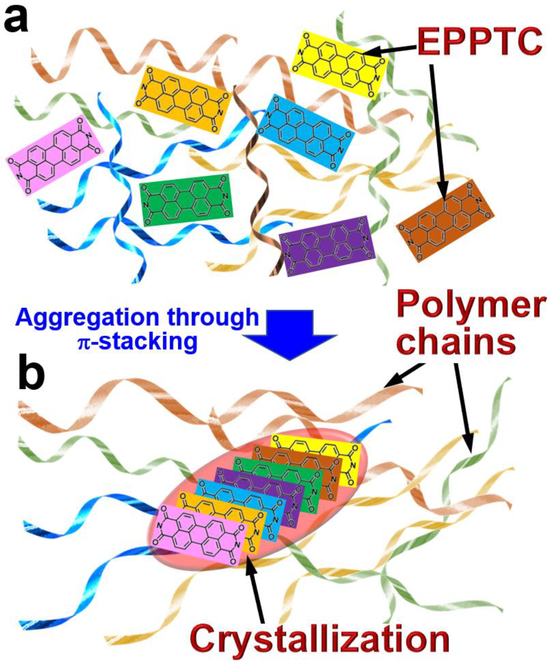
2. Annealing-Aided Crystallization of Small Molecules in Polymeric Solids

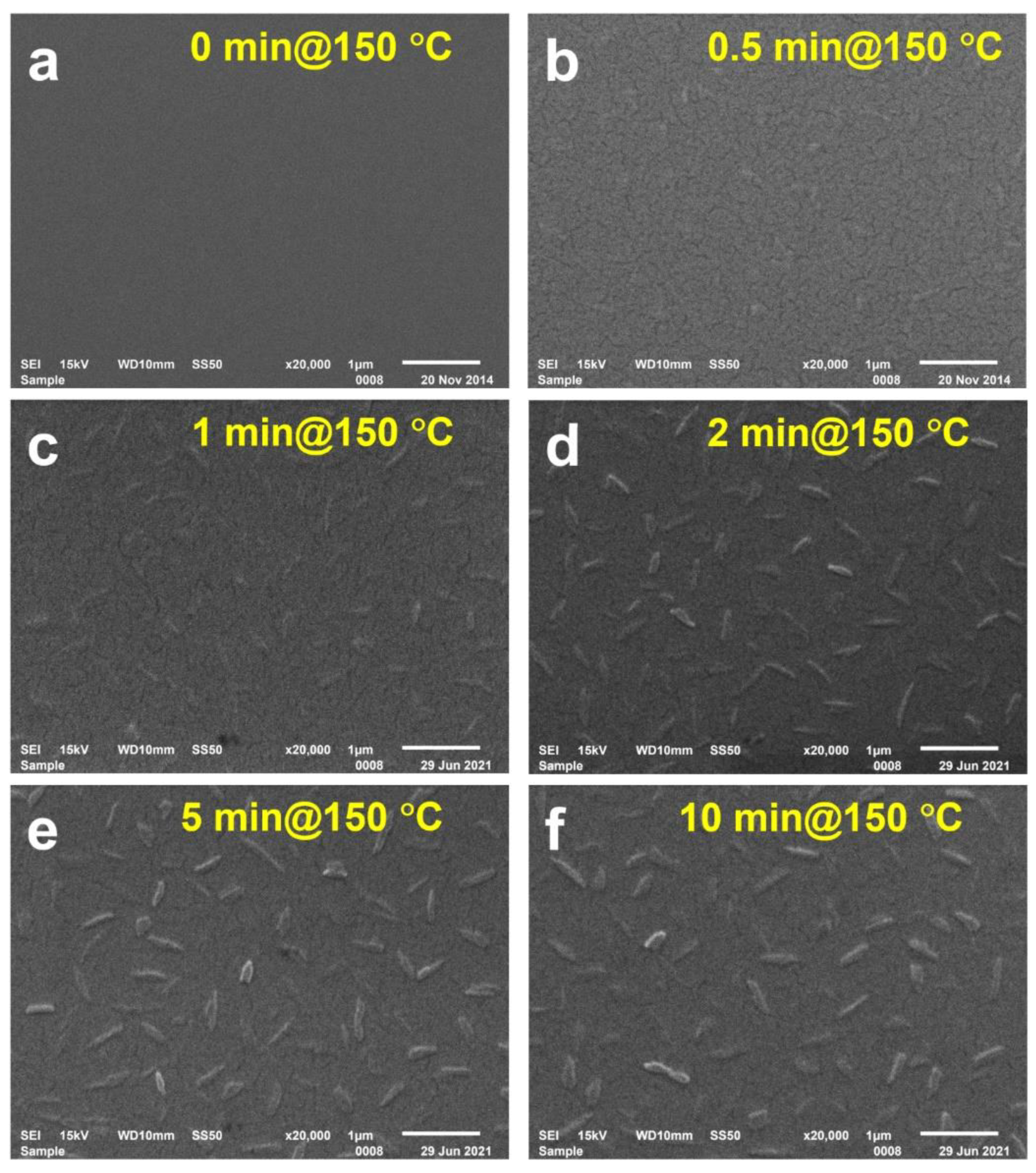
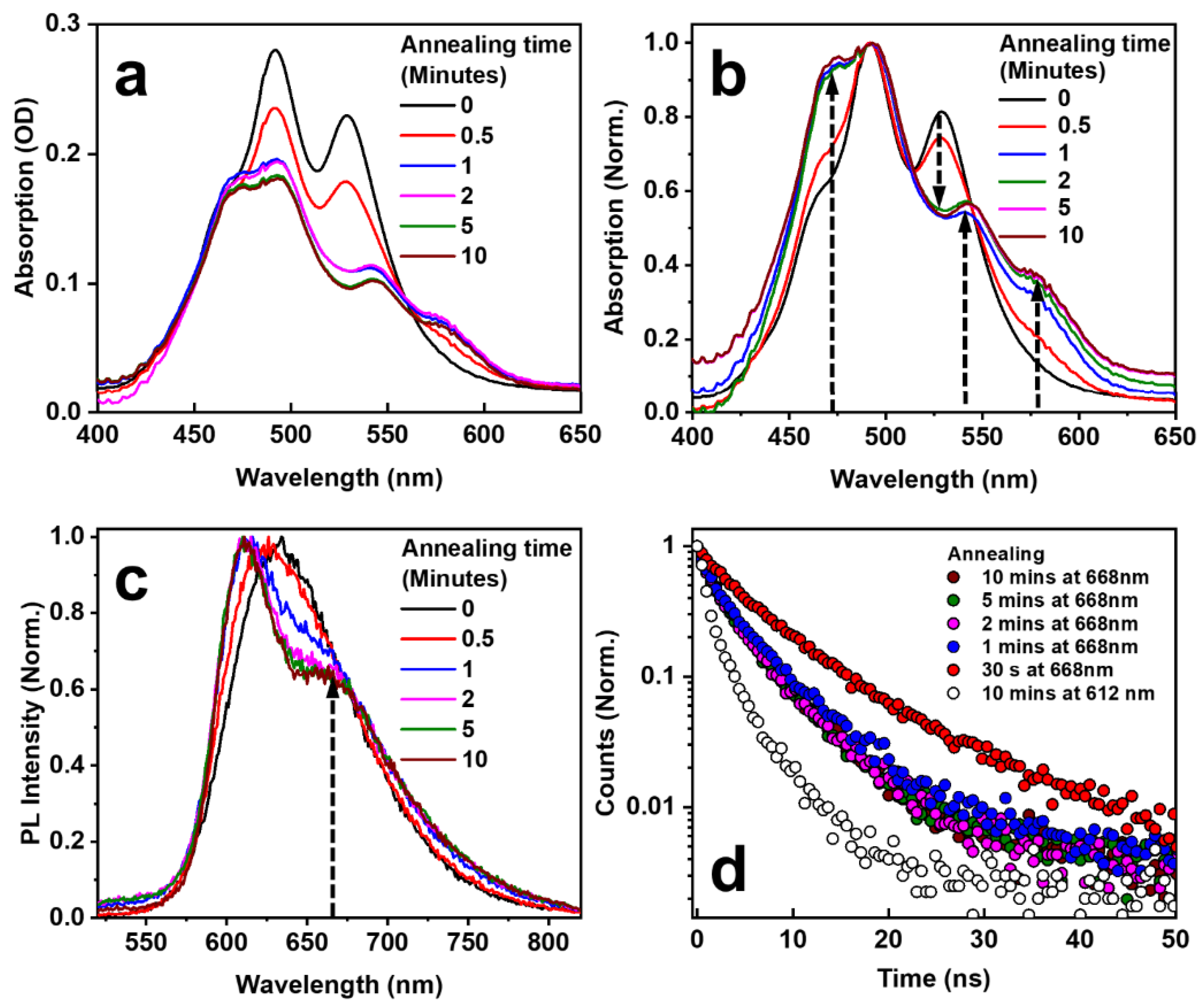
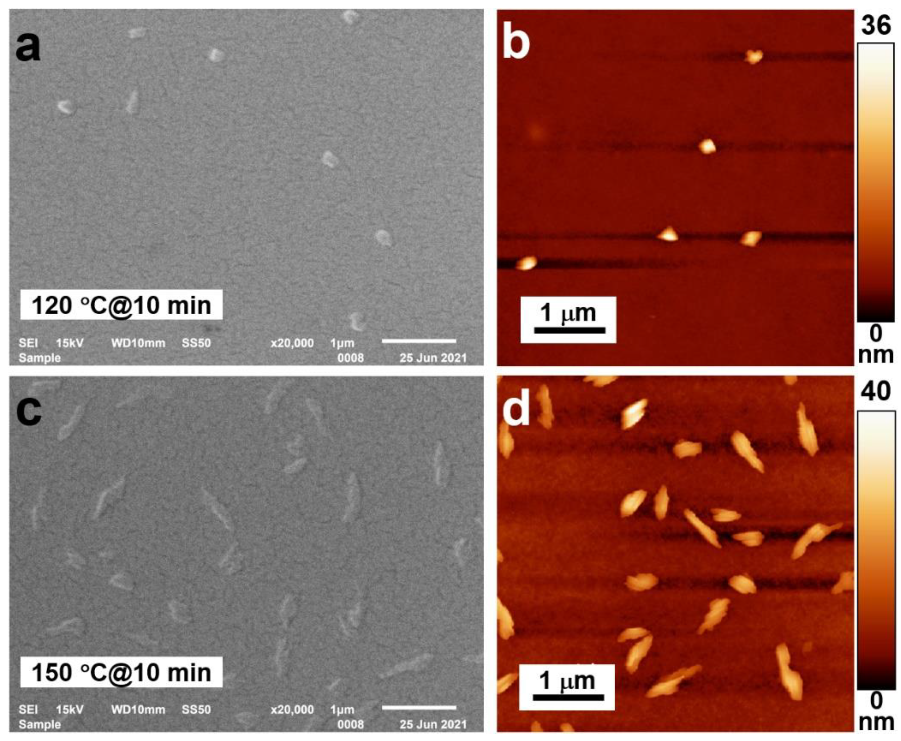
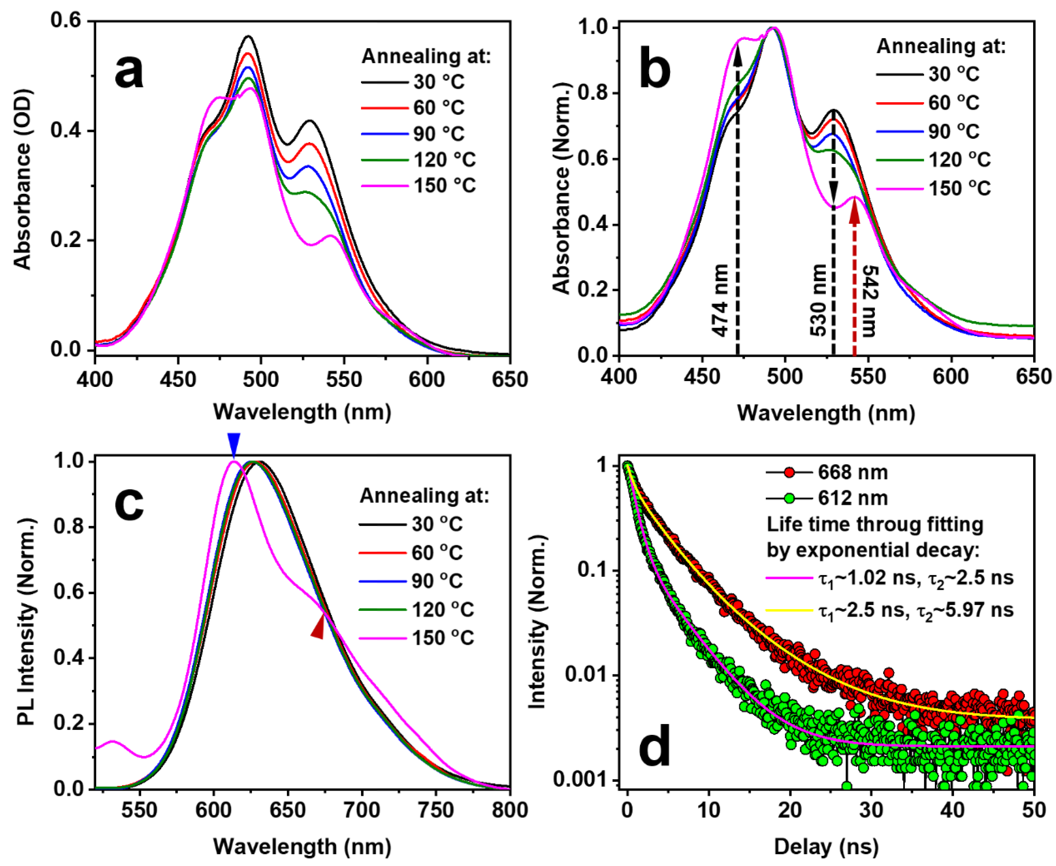
2.1. Annealing Temperature Dependence

In the experiments, we first prepared solutions of EPPTC and PMMA in chloroform with a concentration of 10 mg/mL and 15 mg/mL, respectively. A mixture solution was prepared by mixing the above two solutions with a volume-to-volume ratio of 1:1. A blend film was then prepared by spin-coating the mixture solution onto a glass substrate with a speed of 2000 rpm for 30 s. Multiple samples were prepared under the same conditions so that comparison could be made between different annealing processes.
For the annealing, we employed five temperatures: 30, 60, 90, 120, and 150 °C. However, for annealing temperatures below 120 °C, nearly no changes were observed either in the microscopic or in the spectroscopic response of the sample. This is clearly because the glass transition temperature was not reached. In Figure 2, we present only the scanning electron microscope (SEM, JEOL, Tokyo, Japan) and atomic force microscope (AFM, Witec GmbH, Ulm, Germany) images of the samples annealed at 120 and 150 °C. The SEM and AFM images of the sample annealed at 120 °C are shown in Figure 2a,b, respectively. Since the annealing temperature is already above the threshold for glass transition, crystal particles with very small sizes and very low densities can be observed in both images. The mean diameter of the crystal particles is roughly 140 nm. We need to note that the annealing time was 10 min and the size and density of the crystal particles may be increased by extending the annealing time. Thus, it is verified that the glass transition temperature is the threshold for the crystallization of EPPTC molecules, where the softened PMMA molecular chains allow the movement of the EPPTC molecules and their aggregation through π-stacking.
When the annealing temperature was increased to 150 °C, for the same annealing time of 10 min, the crystal length and thickness were increased dramatically, as shown by the SEM and AFM images in Figure 2c,d, respectively. Using a rough evaluation, the crystals have a mean length of about 900 nm and a width of 160 nm. Meanwhile, the height of the crystals was also increased slightly from about 36 to 40 nm. Furthermore, the density of the crystal particles was more obviously increased. According to Figure 2c,d, the number of crystal particles was increased by a factor of five, corresponding to an increase in the total number of crystal particles from about 6 to 30. This implies convincingly that above the glass transition temperature the PMMA molecules become more flexible and allow the strong aggregation of the EPPTC molecules into crystals.
It is also understood that the crystal particles formed by molecular aggregation through π-stacking greatly influence the spectroscopic properties of the small molecules. Figure 3a shows the absorption spectra at different annealing temperatures, and Figure 3b,c show the normalized data in Figure 3a and the PL spectra of the blend film, respectively, for different annealing temperatures. As the temperature was increased from 30 to 120 °C, where the annealing time was 10 min, a weak feature appeared at about 474 nm and the relative intensity at 530 nm was reduced, as shown in Figure 3b. However, when the temperature was increased to 150 °C, which exceeds the glass transition temperature, the spectral feature became obvious at 473 nm (dashed upward arrow in black) and the peak at about 530 nm suddenly became a valley in the absorption spectrum (dashed downward arrow), as shown in Figure 3b. Furthermore, the absorption spectrum peak at about 542 nm appeared in a sudden manner (dashed upward arrow in red). All of these changes highlighted by dashed arrows resulted from the aggregation of the EPPTC molecules in the softened PMMA film, or from the crystallization through π-stacking of the EPPTC molecules.
Figure 3c shows the PL spectra annealed at 30, 60, 90, 120, and 150 °C for 10 min, where all spectra have been normalized. Obviously, with an annealing temperature lower than 120 °C, there is little change in the PL spectra. However, when the annealing temperature exceeds 150 °C, the PL spectrum changed dramatically: the main peak shifts from about 630 nm to 612 nm (blue triangle) and a new peak appears at about 668 nm (red triangle). According to our previous work [17], the emission at 612 nm corresponds mainly to the intrinsic molecular emission from EPPTC and that at 668 nm mainly to the crystal phase emission. Figure 3d shows the measurements of the emission dynamics at 612 and 668 nm using green and red circles, respectively. At 612 nm, the emission lifetime is in the range of 1~2.5 ns. However, the lifetime extends to about 6 ns at 668 nm, which can be identified as the lifetime of the emission from EPPTC crystal phase. Therefore, the spectroscopic response confirms the crystallization of the EPPTC molecules doped in the PMMA solid film when the sample is annealed at a temperature above the glass transition threshold. It needs to be noted that since the glass transition temperature is different for different polymers and for polymers with different molecular weights, the annealing strategy should be modified for different polymer materials.

2.2. Annealing Time Dependence

At a temperature above the glass transition threshold of PMMA, it takes time for the EPPTC molecules to become aggregated into crystal particles. Figure 4 shows the SEM images of the sample annealed at 150 °C for different times. Before annealing, no crystal particles can be observed in Figure 4a, implying that no crystallization process took place before annealing. Crystal particles can be resolved in Figure 4b for an annealing time of 30 s, although they are small and appear with a low density. For an annealing time longer than 1 min, EPPTC crystal particles can be observed clearly on the surface of the PMMA film. Figure 4c–f show the SEM images for annealing times of 1, 2, 5, and 10 min, respectively. Obviously, both the size and density of the EPPTC crystal particles increase dramatically with increased annealing time. The crystal particles can be clearly resolved only for an annealing time longer than 2 min, and the morphology of the surface of the solid film remains nearly constant when the sample is annealed for more than 5 min. The mean width and length of the crystals are roughly the same as those demonstrated in Figure 2c,d. It is also clearly observable in Figure 4 that the crystals are distributed randomly with random orientations, and that each particle contains inhomogeneous structures, implying that the crystal particles are not single crystals.
Figure 5 shows the spectroscopic characterization of the EPPTC-doped PMMA thin film sample, which was annealed at 150 °C for different times. Figure 5a,b show the directly measured and normalized absorption spectra, respectively. The main absorption peak at about 490 nm did not change its spectral position during the whole process. At least four other new features can be observed with increased annealing time, as highlighted by the dashed arrows in Figure 5b. The absorption peak around 473 nm was enhanced with increased annealing time, while that at about 530 nm is reduced and a new peak appeared at 542 nm; these features are similarly observed in Figure 3b. However, the most obvious difference between Figure 3b and Figure 5b is the spectral peak at about 578 nm, which was observed clearly when the annealing time was longer than 1 min. Therefore, this is the more typical absorption spectrum of the crystal phase.
As has been discussed with regard to Figure 3c, the PL spectrum becomes separated into two components for an annealing temperature of 150 °C. This is again observed in Figure 5c where the annealing time is longer than 1 min, which agrees with the observation of the time-dependent absorption in Figure 5b. The spectral feature peaked at a longer wavelength of 668 nm; this resulted from the crystal phase emission, as highlighted by the dashed arrow in Figure 5c. The difference between the crystal phase emission and the intrinsic molecular emission lies not only in their spectral positions but also in their lifetimes. This is shown in Figure 5d, where we demonstrate the PL dynamics at 612 and 668 nm for different annealing times. Clearly, the emission from the crystal phase at 668 nm is much longer than that from the intrinsic emission from EPPTC molecules.
From Figure 5d, we can also observe that the longest emission lifetime corresponds to an annealing time of 30 s at 150 °C, and that emission lifetime reduces with increased annealing time. For an annealing time longer than 1 minute, the decay dynamics of the emission remain nearly constant. This implies that there exists an intermediate state for the formation of the crystal phase with less quenching of the photoluminescence due to intermolecular interactions. However, after 10 min of annealing, the intrinsic EPPTC emission is much quenched due to the intermolecular interaction in the crystal phase; therefore, emission lifetimes at 612 and 668 nm are both reduced. The lifetime values become fixed after the equilibrium of the crystallization process is reached at a specified annealing temperature for a sufficiently long annealing time. We can also identify clearly from Figure 5d that the emission lifetime at 668 nm is much longer than that at 612 nm, implying long-lived crystal phase emissions, as compared with the intrinsic EPPTC molecular emissions, verifying the formation of the π-stacked crystals.

3. Conclusions

We have demonstrated in this experimental work that it is possible for small molecular semiconductors to move and aggregate into crystal phases in a solid film of polymers, as long as the polymer film is softened and flexibilized, e.g., through heating it to its glass transition temperature. We verified such mechanisms using EPPTC molecules doped in a PMMA thin film. Both the microscopic and spectroscopic evaluations justified the validness of the proposed mechanisms and characterized the properties of the crystalized materials/structures. We can thus conclude that heterojunctions based on blends of small molecules and polymers can be constructed and modified by a low-temperature annealing process after production of the solid film, which simplifies the preparation and enables high-quality thin-film devices to be produced. Therefore, this strategy is important for the design and realization of organic optoelectronic devices based on blend materials or heterojunction structures.

Author Contributions

Conceptualization, X.Z.; Formal analysis, X.Z.; Funding acquisition, X.Z.; Investigation, Y.L. and X.Z.; Methodology, X.Z.; Project administration, X.Z.; Resources, X.Z.; Supervision, X.Z.; Writing—original draft, X.Z.; Writing—review & editing, X.Z. All authors have read and agreed to the published version of the manuscript.

Funding

This research was funded by National Natural Science Foundation of China, grant number 61735002 and 12074020 and by Beijing Municipal Education Commission, grant number KZ202010005002. The APC was funded by National Science Foundation of China.

Institutional Review Board Statement

Not applicable.

Informed Consent Statement

Not applicable.

Data Availability Statement

Not applicable.

Acknowledgments

The authors acknowledge the National Natural Science Foundation of China (61735002, 12074020) and Beijing Municipal Education Commission (KZ202010005002) for their support.

Conflicts of Interest

The authors declare no conflict of interest.

References

  1. Nguyen, T.-Q.; Martel, R.; Avouris, P.; Bushey, M.L.; Brus, L.; Nuckolls, C. Molecular Interaction in One-Dimensional Organic nanostructures. J. Am. Chem. Soc. 2004, 126, 5234. [Google Scholar] [CrossRef]
  2. Karl, N.; Kraft, K.-H.; Marktanner, J.; Munch, M.; Schatz, F.; Stehle, R.; Uhde, H.-M. Fast electronic transport in organic molecular solids? J. Vac. Sci. Technol. A 1999, 17, 2318. [Google Scholar] [CrossRef]
  3. Hill, J.P.; Jin, W.; Kosaka, A.; Fukushima, T.; Ichihara, H.; Shimomura, T.; Ito, K.; Hashizume, T.; Ishii, N.; Aida, T. Self-assembled hexa-peri-hexabenzocoronene graphitic nanotube. Science 2004, 304, 1481. [Google Scholar] [CrossRef] [Green Version]
  4. Mas-Torrent, M.; Durkut, M.; Hadley, P.; Ribas, X.; Rovira, C. High Mobility of Dithiophene-Tetrathiafulvalene Single-Crystal Organic Field Effect Transistors. J. Am. Chem. Soc. 2004, 126, 984. [Google Scholar] [CrossRef] [Green Version]
  5. de Boer, R.W.I.; Gershenson, M.E.; Morpurgo, A.F.; Podzorov, V. Organic single-crystal field-effect transistors. Phys. Stat. Solidi A 2004, 201, 1302. [Google Scholar] [CrossRef] [Green Version]
  6. Xu, B.; Xiao, X.; Yang, X.; Zang, L.; Tao, N. Large gate modulation in the current of a room Temperature single molecule transistor. J. Am. Chem. Soc. 2005, 127, 2386. [Google Scholar] [CrossRef]
  7. Schmidt-Mende, L.; Fechtenkoetter, A.; Muellen, K.; Moons, E.; Friend, R.H.; Mackenzie, J.D. Self-organized discotic liquid crystals for high-efficiency organic photovoltaics. Science 2001, 293, 1119. [Google Scholar] [CrossRef] [Green Version]
  8. Ohisa, S.; Pu, Y.; Yamada, N.; Matsuba, G.; Kido, J. Influence of solution- and thermal-annealing processes on the sub-nanometer-ordered organic–organic interface structure of organic light-emitting devices. Nat. Commun. 2017, 9, 25–30. [Google Scholar] [CrossRef]
  9. Wuerthner, F. Perylene bisimide dyes as versatile building blocks for functional supermolecular architechtures. Chem. Commun. 2004, 2004, 1564–1579. [Google Scholar] [CrossRef]
  10. Lee, B.; Park, O. The effect of different heat treatments on the luminescence efficiency of polymer light-emitting diodes. Adv. Mater. 2000, 12, 801–804. [Google Scholar] [CrossRef]
  11. Ahn, J.; Wang, C.; Widdowson, N.; Pearson, C.; Bryce, M.; Petty, M. Thermal annealing of blended-layer organic light-emitting diodes. J. Appl. Phys. 2005, 98, 054508. [Google Scholar] [CrossRef]
  12. Sajjad, M.; Zhang, Y.; Geraghty, P.; Mitchell, V.; Ruseckas, A.; Blaszczyk, O.; Jones, D.; Samuel, I. Tailoring exciton diffusion and domain size in photovoltaic small molecules by annealing. J. Mater. Chem. C 2019, 7, 7922–7928. [Google Scholar] [CrossRef]
  13. Tanaka, H.; Abe, Y.; Matsuo, Y.; Kawai, J.; Soga, I.; Sato, Y.; Nakamura, E. An amorphous mesophase generated by thermal annealing for high-performance organic photovoltaic devices. Adv. Mater. 2012, 24, 3521–3525. [Google Scholar] [CrossRef]
  14. Jaqadamma, L.; Sajjad, M.; Savikhin, V.; Toney, M.; Samuel, I. Correlating photovoltaic properties of a PTB7-Th:PC71BM blend to photophysics and microstructure as a function of thermal annealing. J. Mater. Chem. A 2017, 5, 14646–14657. [Google Scholar] [CrossRef] [Green Version]
  15. Zhang, T.; Han, H.; Zou, Y.; Lee, Y.; Oshima, H.; Wong, K.; Holmes, R. Impact of thermal annealing on organic photovoltaic cells using regioisomeric donor-acceptor-acceptor molecules. ACS Appl. Mater. Interfaces 2017, 9, 25418–25425. [Google Scholar] [CrossRef]
  16. Yan, B.; Swaraj, S.; Wang, C.; Hwang, I.; Greenham, N.; Groves, C.; Ade, H.; Mcneill, C. Influence of annealing and interfacial roughness on the performance of bilayer donor/acceptor polymer photovoltaic devices. Adv. Funct. Mater. 2010, 20, 4329–4337. [Google Scholar] [CrossRef]
  17. Zhang, X.P.; Sun, B.Q. Organic crystal fibers aligned into oriented bundles with polarized emission. J. Phys. Chem. B 2007, 111, 10881–10885. [Google Scholar] [CrossRef]
  18. van Herrikhuyzen, J.; Syamakumari, A.; Schenning, A.P.H.J.; Meijer, E.W. Synthesis of n-type perylene bisimide derivatives and their orthogonal self-assembly with p-type oligo(p-phenylene vinylene)s. J. Am. Chem. Soc. 2004, 126, 10021. [Google Scholar] [CrossRef]
  19. Mascaro, D.J.; Thompson, M.E.; Smith, H.I.; Bulovic, V. Forming oriented organic crystals from amorphous thin films on patterned substrates via solvent-vapor annealing. Org. Electron. 2005, 6, 211. [Google Scholar] [CrossRef]
  20. Zhang, X.P.; Dou, F.; Liu, H.M. Charge-Transfer Complex Coupled Between Polymer and H-Aggregate Molecular Crystals. J. Polym. Sci. B: Polym. Phys. 2013, 51, 749–755. [Google Scholar] [CrossRef]
  21. Garner, L.E.; Viswanathan, V.N.; Arias, D.H.; Brook, C.P.; Christensen, S.T.; Ferguson, A.J.; Kopidakis, N.; Larson, B.W.; Owczarczyk, Z.R.; Pfeilsticker, J.R.; et al. Photobleaching dynamics in small molecule vs. polymer organic photovoltaic blends with 1,7-bis-trifluoromethylfullerene. J. Mater. Chem. A 2018, 6, 4623. [Google Scholar] [CrossRef]
  22. Li, H.; Lu, K.; Wei, Z.X. Polymer/small molecule/fullerene based ternary solar cells. Adv. Energy Mater. 2017, 7, 1602540. [Google Scholar] [CrossRef]
Figure 1. (a) Distribution of the EPPTC molecules in the solid film of PMMA molecular chains. (b) Crystallization of EPPTC small molecules due to their motion across the annealing-flexibilized PMMA molecular chains.
Crystals 11 01022 g001
Figure 2. SEM (a,c) and AFM (b,d) images for the samples annealed at 120 (a,b) and 150 °C (c,d).
Crystals 11 01022 g002
Figure 3. (a) Absorption spectra measured at different annealing temperatures. (b) Normalized absorption spectra in (a). (c) Normalized PL spectra measured at different annealing temperatures. (d) Fluorescence lifetime at 612 (blue triangle in (c)) and 668 nm (red triangle in (c)) for the sample annealing at 150 °C for 10 min.
Crystals 11 01022 g003
Figure 4. SEM images at an annealing temperature of 150 °C for (a) 0, (b), 0.5, (c) 1, (d) 2, (e) 5, and (f) 10 min.
Crystals 11 01022 g004
Figure 5. Absorption (a,b) and PL (c) spectra of the blend film annealed at 150 °C for different annealing times. (b) A normalized replot of (a). (d) Emission decay dynamics at 668 nm for different annealing times of 0.5, 1, 2, 5, 10 min and a comparison with that at 612 nm for an annealing time of 10 min.
Crystals 11 01022 g005
Publisher’s Note: MDPI stays neutral with regard to jurisdictional claims in published maps and institutional affiliations.

