Article

High-Performance Flexible Transparent Electrodes Fabricated via Laser Nano-Welding of Silver Nanowires

1
Faculty of Science, Beijing University of Technology, Beijing 100124, China
2
Faculty of Materials and Manufacturing, Beijing University of Technology, Beijing 100124, China
*
Author to whom correspondence should be addressed.
Equal contribution to this work.
Crystals 2021, 11(8), 996; https://doi.org/10.3390/cryst11080996
Submission received: 7 August 2021 / Revised: 18 August 2021 / Accepted: 18 August 2021 / Published: 21 August 2021

Abstract

:
Silver nanowires (Ag-NWs), which possess a high aspect ratio with superior electrical conductivity and transmittance, show great promise as flexible transparent electrodes (FTEs) for future electronics. Unfortunately, the fabrication of Ag-NW conductive networks with low conductivity and high transmittance is a major challenge due to the ohmic contact resistance between Ag-NWs. Here we report a facile method of fabricating high-performance Ag-NW electrodes on flexible substrates. A 532 nm nanosecond pulsed laser is employed to nano-weld the Ag-NW junctions through the energy confinement caused by localized surface plasmon resonance, reducing the sheet resistance and connecting the junctions with the substrate. Additionally, the thermal effect of the pulsed laser on organic substrates can be ignored due to the low energy input and high transparency of the substrate. The fabricated FTEs demonstrate a high transmittance (up to 85.9%) in the visible band, a low sheet resistance of 11.3 Ω/sq, high flexibility and strong durability. The applications of FTEs to 2D materials and LEDs are also explored. The present work points toward a promising new method for fabricating high-performance FTEs for future wearable electronic and optoelectronic devices.

1. Introduction

High-performance flexible transparent electrodes (FTEs) with outstanding mechanical and optical properties facilitate the rapid development of wearable electronics and optoelectronics [1]. Compared with rigid materials such as silicon and silica, elastic substrates make the devices foldable, twistable, compressible, and stretchable without compromising stability and reliability, allowing for a wide range of applications, including flexible electronic displays, organic light-emitting diodes (OLEDs), solar cells, and electronic skins [2,3,4,5]. FTEs are critical components in the above-mentioned wearable devices to ensure a high-efficiency power supply with low energy consumption. Moreover, the excellent optical transmittance would replace indium tin oxide (ITO) for next-generation, highly flexible optoelectronic applications, overcoming the drawbacks of time-consuming synthesis, indium requirement, and fragility during stretching and bending. In recent decades, numerous efforts have been made to develop alternative FTEs, including graphene [6,7,8], nanowires [9,10,11,12], carbon nanotubes (CNTs) [13,14,15], and PEDOT:PSS [16,17,18].
Silver nanowires (Ag-NWs) have attracted considerable attention as FTE materials owing to their good electrical conductivity, high transparency in the visible band, excellent ductility, and facile fabrication process [19]. In particular, the conductive networks formed by ultralong metallic nanofibers have shown promise for application to FTEs because of their superior optical, electrical, and mechanical properties [20,21]. A variety of electronic components with Ag-NW FTEs were fabricated in previous studies, including flexible and transparent antennas [22], wireless circuits [23], transistors [24], and sensors [25], demonstrating the potential applications in wearable devices. However, the contact resistance between Ag-NWs and adhesion to the organic substrates have presented two major challenges for high-performance FTEs. Methods for the improvement of contact resistances have been sophisticatedly presented in previous works. Thermal annealing has received the most attention due to its facile fabrication process and high welding quality. However, thermal annealing requires an oxygen-free environment due to the high chemical reactivity of Ag-NWs at high temperature. Moreover, thermal annealing is not suitable for the flexible organic substrates due to the low melting temperature of organic materials. Consequently, a low-temperature thermal annealing (below 200 °C) was developed [26]. Other physical welding methods employing force, electricity, light, etc. were also developed to realize Ag-NW network welding without significant thermal effects for FTEs [27,28,29,30,31,32,33,34,35]. Although high-pressure welding optimized the conductivity of the Ag-NW FTEs down to 8.4 Ω/sq, the substrates and other layers could be destroyed [27]. To solve this problem, Liu et al. proposed a capillary-force-induced cold-welding technique in which the moisture-treated Ag-NWs exhibited a significant reduction in sheet resistance (~37 Ω/sq) due to the giant capillary forces exerted between Ag-NWs [28]. Unfortunately, the poor adhesion of Ag-NWs on the substrate has not been improved. Another method that has been used is electric welding; it is based on the high contact resistance at the junction of Ag-NWs, where Joule heating caused by the application of bias voltages results in localized melting, welding the Ag-NWs [29]. The main drawback of this method is the non-homogeneous current distribution due to the complex Ag-NW network, which proved unsuitable for large-area welding. Hong et al. achieved Ag-NW nano-welding by electron-beam irradiation, which provided sufficient energy to melt the Ag-NWs [30]. However, the required vacuum chamber and the high-cost instrument limited the method for industrial applications. Compared with electron beams, light is an ideal energy source to induce the nano-welding of Ag-NWs. Liang et al. employed ultraviolet A (UVA) light irradiation for Ag-NW nano-welding, reducing the sheet resistance by three orders of magnitude (down to 25 Ω/sq) with a good transparency (97%) [31]. The femtosecond pulsed laser (fs-pulsed laser) was also used to irradiate Ag-NWs, where the excited localized surface plasmon resonances (LSPRs) at the gaps between Ag-NWs generated a considerable enhancement of electric field strength, inducing local melting for nano-welding. Meanwhile, the polyethylene glycol terephthalate (PET) substrate was not damaged during the laser irradiation. The obtained sheet resistance and optical transmittance by fs-pulsed nano-welding were 16.1 Ω/sq and 91%, respectively [32]. Although nanosecond pulsed lasers (ns-pulsed lasers) were also tested for the nano-welding of Ag-NWs [33], most of the laser-irradiation methods were only suitable for inorganic and limited organic substrates with high melting temperatures and stiffnesses (glass, silica, PET, PVA), owing to the requirement of thermal endurance from laser energy input. Generally, the most used highly flexible and bio-compatible organic materials (e.g., polydimethylsiloxane, PDMS), possess low melting points and stiffnesses. Therefore, a nano-welding technique for junction-localized energy confinement that will not deteriorate the substrate is still lacking. In addition, the adhesion of Ag-NW networks to the organic substrate also needs to be resolved by jointing Ag-NWs with the substrate gently [9,10].
In this work, we developed a facile technique for fabricating high-performance FTEs via ns-pulsed laser nano-welding of Ag-NWs on organic substrates, creating Ag-NWs/PMMA/PDMS sandwich structures. LSPR-induced laser energy confinement at the junctions between the Ag-NWs was employed to generate a high temperature for nano-welding in order to reduce contact resistances while dramatically boosting the electrical conductivity of the Ag-NWs. Meanwhile, the Ag-NW networks were jointed with the organic substrate for good adhesive strength. The ns-pulsed laser energy for nano-welding was low enough to avoid thermal damage to the organic substrates completely. The fabricated FTEs in this work demonstrated superior mechanical, electrical, and optical properties. The compatibility of FTEs with 2D materials and traditional LEDs was also explored for the design of flexible optoelectronic devices in the future.

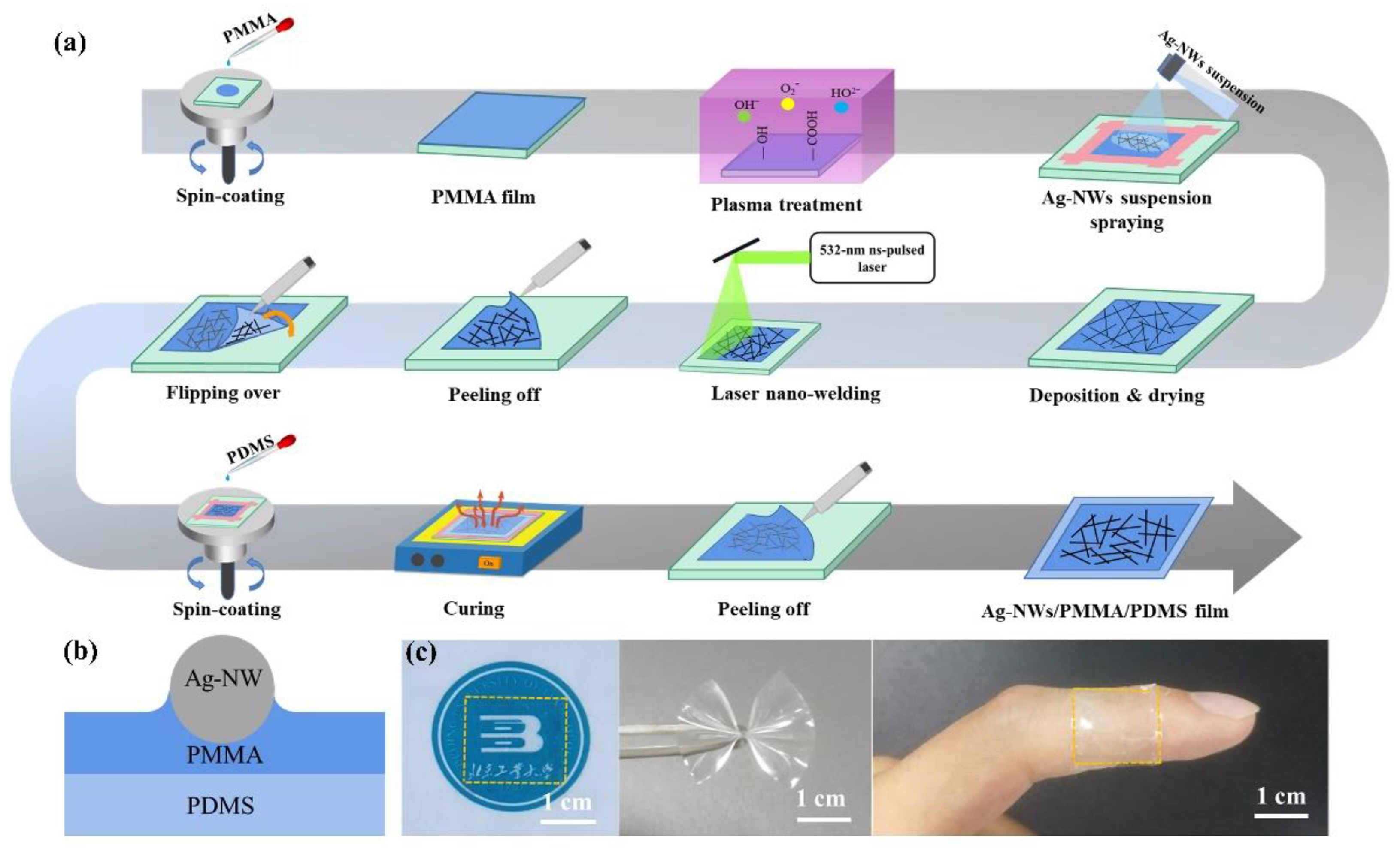
2. Materials and Methods

A schematic of the procedure for fabricating Ag-NW FTEs is illustrated in Figure 1a. The glass substrates (2 cm × 2 cm) were first cleaned ultrasonically in acetone, isopropanol, and deionized water, successively, for 5 min. The polymethyl methacrylate (PMMA) solution in toluene (purchased from Shanghai Kexinda Polymer Materials Co., Ltd., Shanghai, China) was spin-coated onto the glass substrate at 8000 rpm for 40 s to achieve a thickness of ~10 μm, then cured in ambient atmospheric for 10 s. Then, the PMMA film was treated with plasma (YZD08-5C, 80 W, Saiaote Technology Co. Ltd., Wuhu, China) for 30 s to achieve a hydrophilic surface, beneficial for both uniform spreading and the prevention of agglomeration during Ag-NW suspension deposition. The Ag-NWs (purchased from Nanjing XFNANO Co., Ltd., Nanjing, China), with a mean length of ~100 μm and diameter of 30.0 ± 5.0 nm, diluted in isopropyl alcohol (IPA) for various concentrations (0.3–0.7 mg/mL), were sprayed onto the PMMA surfaces. To minimize the coffee-ring effect on Ag-NWs deposition, 3M low-adhesion tapes were employed to confine the suspension flow within a specific region. The homogeneous Ag-NWs were therefore formed after the suspension was dried. The densities of Ag-NWs on PMMA films were controlled by two synthesis parameters: the concentration of the Ag-NWs suspension (0.3–0.7 mg/mL) and the number of spraying layers (5–20 layers). Afterwards, the Ag-NWs/PMMA film was irradiated by a 532 nm ns-pulsed laser (Spectra-Physics, LAB-190-30H, 10 ns, 27 Hz) under ambient conditions at room temperature, achieving Ag-NW nano-welding and jointing with the PMMA substrate. It should be noted that the highly transparent PMMA with respect to 532 nm (95%) and the short pulse duration minimized the thermal damage on the substrate within the irradiation time of 50 s. The oxidation of Ag-NWs during laser irradiation was also negligible. The PDMS Sylgard 184 (purchased from Dow corning Co., Ltd., Midland, MI, USA) was mixed and stirred with the curing agent at the ratio of 10:1 by weight to obtain the PDMS colloidal solution. The fabricated Ag-NWs/PMMA film was then flipped over on the spinner. The PDMS solution was spin-coated onto the bottom side of the Ag-NWs/PMMA film at a rotation speed of 5000 rpm for 30 s. The PDMS film was baked at 120 °C for 2 min on a plate heater in a vacuum chamber for solidification and bubble removal. The Ag-NWs/PMMA/PDMS film was therefore obtained, where the thickness of the PDMS film was ~20 μm. It should be noted that the PDMS film provided an outstandingly flexible substrate for the FTEs, and the plasma-treated PMMA film served as a buffer layer for high adhesion of Ag-NWs and PDMS in the sandwich structure, as shown in Figure 1b. Figure 1c demonstrates the optical and mechanical performance of the Ag-NWs/PMMA/PDMS FTEs. In addition, the MoS2 monolayer (purchased from Shenzhen Six-Carbon Technology, Shenzhen, China), grown on an n-type Si substrate with a 300 nm-thick SiO2 film, was also employed for future experiments.
The sheet resistances were measured using the four-point probe method (Suzhou Jingge Electronic Co., Ltd., ST2258C, Suzhou, China), in which the mean values of sheet resistances from six random points of the FTEs were calculated. The optical transmittances of the FTEs were obtained by a UV-VIS spectrophotometer (Shimadzu, UV-3600, Kyoto, Japan). The morphologies of the Ag-NWs in the FTEs were captured by optical microscopy (Olympus BX-51, Tokyo, Japan), scanning electron microscopy (Hitachi, SU8220, Tokyo, Japan), and transmission electron microscopy (FEI, Tecnai G2-20-S-TWIN, Lausanne, Switzerland). The film thickness was acquired by a profilometer (Veeco Dektak-XT, Bruker, Billerica, MA, USA). The gate-voltage applied to the MoS2 was supplied by a DC power supply (Beijing leading Hongzhi Electronic Technology Co., Ltd., XD1715A-120, Beijing, China). The photoluminescence spectra were analyzed by a SmartRaman confocal-micron-Raman system (developed by Institute of Semiconductors, CAS, Beijing, China) with a 10x/NA0.25 objective lens (Olympus, MPlan N, Tokyo, Japan) under the backscattering geometry, which was coupled with a Horiba LabRam iHR550 spectrometer (Kyoto, Japan) with a 100 lines/mm grating and a CCD detector. The excitation CW laser wavelength was 633 nm (HNL 100-EC-PS, 25.8 μW, Changchun New Industries Technology Co., Ltd., Changchun, China). The electrical power supply and current measurement for LEDs were provided by a source meter (Keithley 4200-SCS, Tektronix, Beaverton, OR, USA).
The numerical simulation was performed using the finite element algorithm method in the COMSOL Multiphysics (licensed by COMSOL Co., Ltd., Stockholm, Sweden) software package. A 2D cross-sectional model was developed to calculate the electric fields regulated at the cross-junctions and gaps between Ag-NWs. The Ag-NW diameter was 30 nm, and the relative permittivity was −9.3751 + 0.83203i according to Drude’s model. The ambient environment was set as air. For the analysis of electric field enhancement, a plane wave with a wavelength of 532 nm was incident onto the Ag-NWs. Perfectly matched layers were applied as the boundary conditions.

3. Results and Discussion

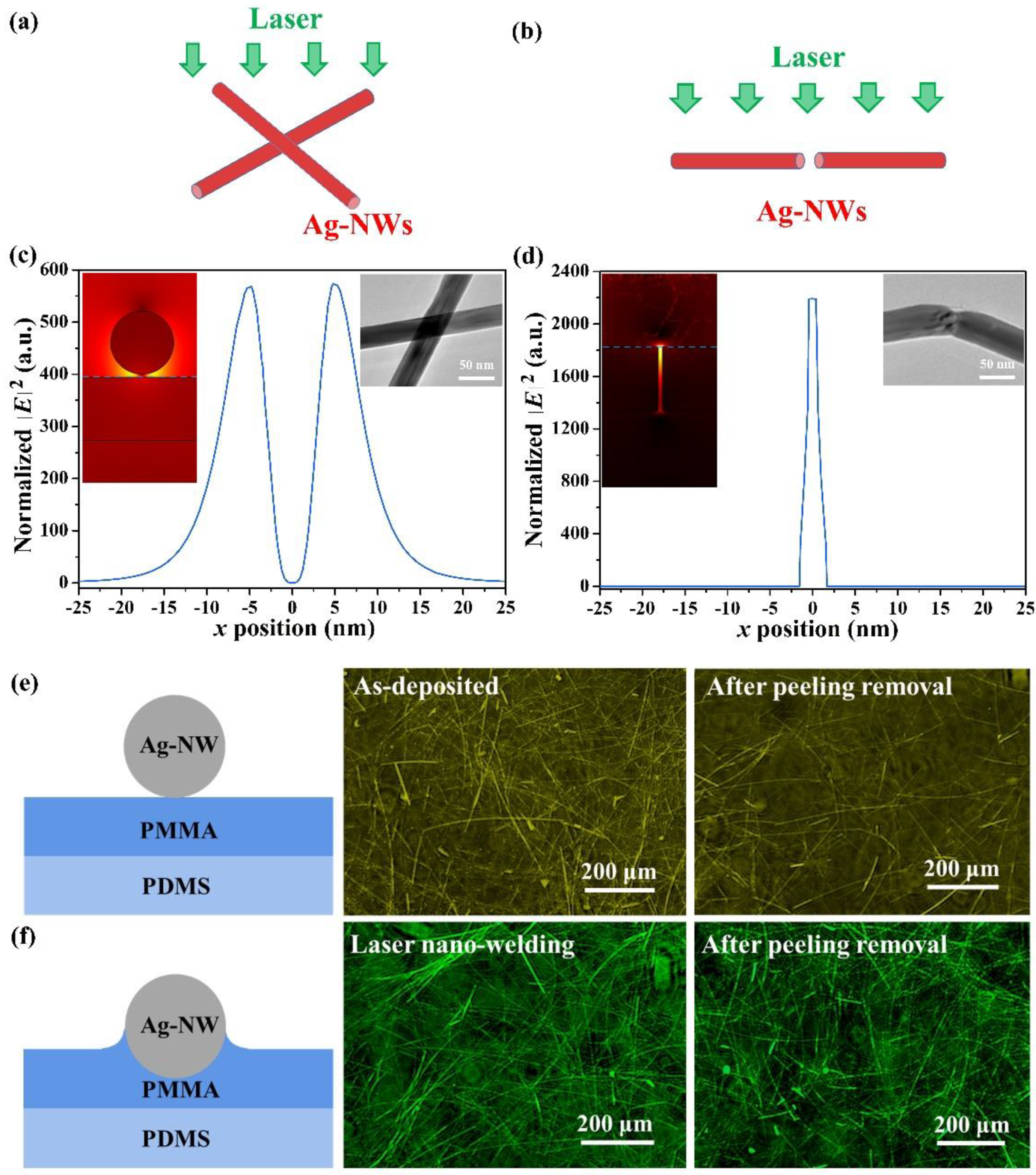
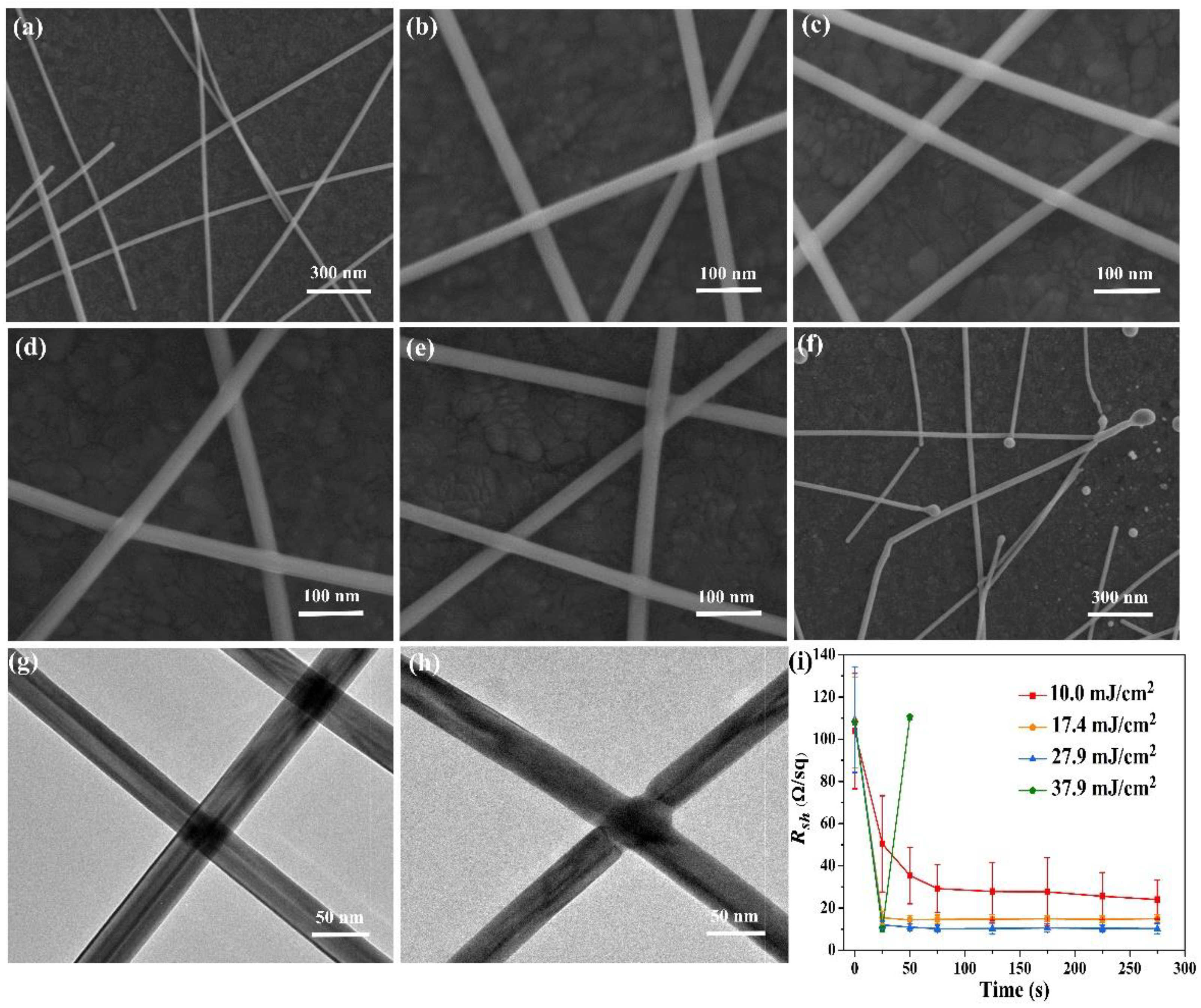
3.1. Morphology of Laser Nano-Welded Ag-NWs

The morphologies of Ag-NWs nano-welded via various laser fluences are shown in Figure 2. The as-deposited Ag-NWs were randomly distributed on the PMMA film, forming a conductive network, as shown in Figure 2a. The close-up view in Figure 2b further demonstrates the cross junctions of the Ag-NWs before laser nano-welding. The contacts between Ag-NWs and with the PMMA substrate were ascribed to van der Waals forces. The fluence threshold for laser nano-welding was ~10.0 mJ/cm2, by which the cross junctions were melted slightly and connected after resolidification. The melting phenomenon became obvious with the laser fluence increasing to 17.4 mJ/cm2. It can be clearly seen in Figure 2c–e that only the cross junctions were melted during laser irradiation whereas the other parts of Ag-NWs were not affected, indicating the laser-induced thermal effect was confined to the contact points. When the laser fluence was greater than 27.9 mJ/cm2, the Ag-NWs sustained thermal damage. The high molten volumes and surface tensile effect broke the Ag-NWs, as shown in Figure 2f. Figure 2g,h further exhibits the welded points before and after laser irradiation, providing strong evidence of Ag-NW melting at the cross junction. To further optimize the laser nano-welding parameters, the effects of laser fluence and irradiation time on sheet resistance were studied, as shown in Figure 2i. The sheet resistance of as-deposited Ag-NWs was 110 Ω/sq and dramatically reduced via laser nano-welding within tens of seconds. The increased laser fluence and irradiation time both lowered the sheet resistance. It can also be seen that the sheet resistances were close to constants dominated by laser fluences as the irradiation time exceeded 50 s. The irradiation time of 50 s was therefore chosen as the optimal parameter to avoid oxidation of the Ag-NWs and thermal damages on the organic substrate. It should be noted that the high sheet resistance with a laser fluence of 37.9 mJ/cm2 at an irradiation time of 50 s was due to the deterioration of the Ag-NWs, as shown in Figure 2f. Hence, the laser fluence was set to 27.9 mJ/cm2 with an irradiation of 50 s for the lowest sheet resistance down to 11.3 Ω/sq, whereby the thermal effect on organic substrates was also negligible.

3.2. Mechanism of Laser Nano-Welding of Ag-NWs on PMMA

To further study the mechanism of laser nano-welding of the Ag-NWs on organic substrates, a numerical simulation of laser interaction with Ag-NWs was performed. Two typical structures of as-deposited Ag-NWs were considered, as illustrated in Figure 3a,b, including cross-junction and head-to-head configurations. It is well-acknowledged that the LSPRs in the vicinity of Ag-NWs can be excited by light with a wavelength of ~500 nm, by which the electromagnetic (EM) fields are significantly enhanced and localized around the Ag-NWs. Meanwhile, the Joule heating caused by ohmic energy loss resulted in melting for the nano-welding of Ag-NWs [36,37,38,39]. The electric fields in the two structures are shown in Figure 3c,d. It can be clearly observed that the electrical intensities were boosted in the gaps between Ag-NWs, where the enhancement ratios were 573.4 and 2193.2 for cross-junction and head-to-head structures, respectively. As a result, these regions were first melted under laser irradiation and connected, realizing Ag-NW welding. The electrical intensities far from these gaps were extremely low, preventing the deterioration of Ag-NWs. The numerical simulation was in agreement with the experimental results, revealing the mechanism of laser nano-welding of the Ag-NWs. Furthermore, selective nano-welding was conducive to Ag-NW network jointing with the PMMA. Owing to its low melting point (~200 °C), the PMMA film can be melted due to the high temperature at the Ag-NW welding regions, and the Ag-NW network was partially embedded into the organic film for good adhesion. To validate the hypothesis, a 3M low-adhesion tape was employed to press and remove the Ag-NWs from the FTEs, as shown in Figure 3e,f. The adhesion between Ag-NWs and PMMA was significantly strengthened after laser nano-welding, as shown by the slight reduction of Ag-NW quantity under removal cycles of over 100. This confirmed the jointing of the Ag-NW network and PMMA substrate by laser irradiation.

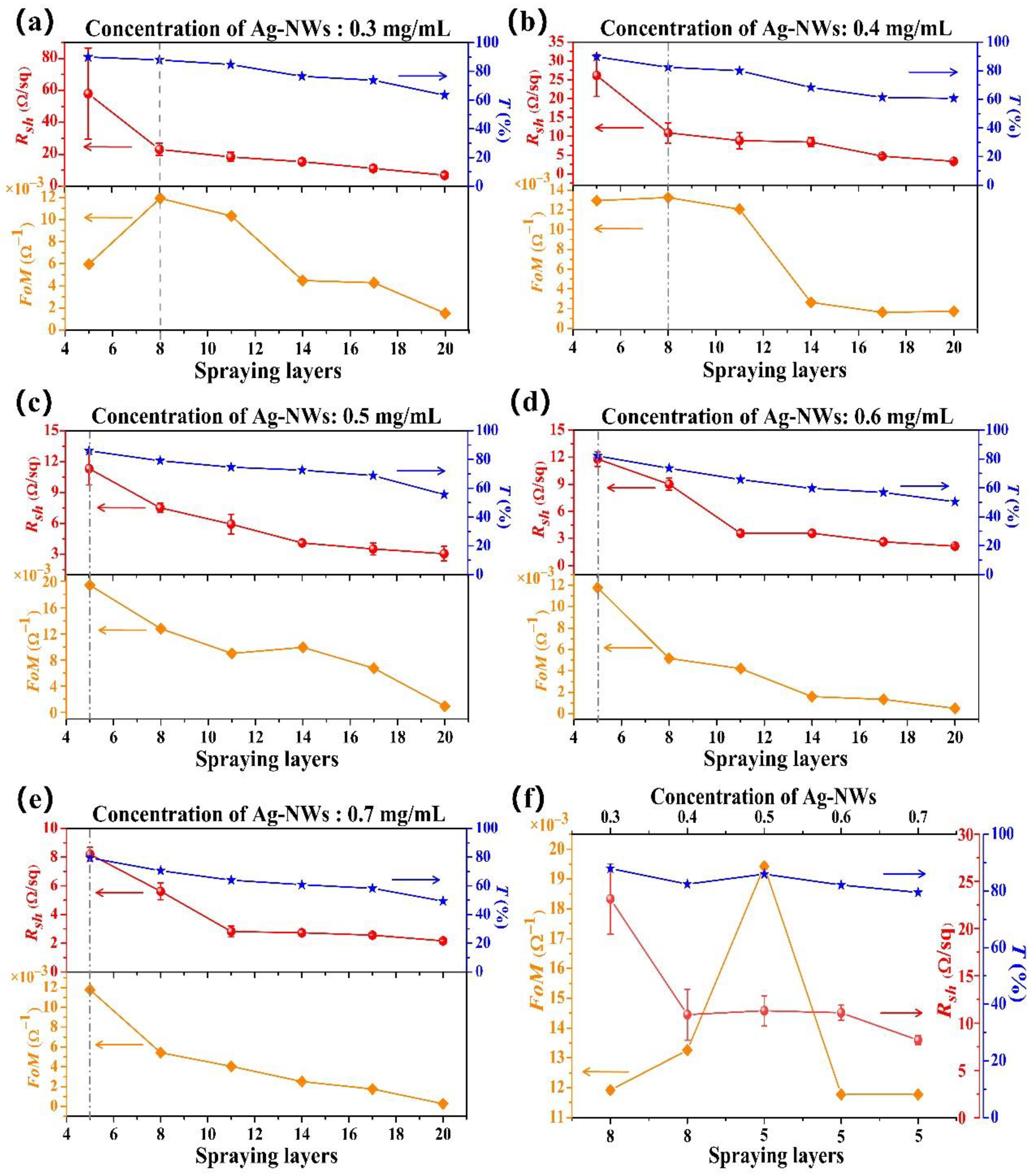
3.3. Synthesis Optimization of Ag-NWs/PMMA/PDMS FTEs

The criteria for high-quality FTEs consist of electrical conductivity and transmittance. The ideal FTEs should possess high conductivity, good transmittance, and durable flexibility. The transmittance was generally reduced as conductivity increased due to light scattering and absorption by the high concentration of Ag-NWs. Therefore, the balance between conductivity and transmittance should be maintained by optimizing the density of Ag-NWs on the PMMA film. The multiple-spraying strategy was therefore employed to control the density by two parameters, that is, the concentration of the Ag-NWs suspension and the number of spraying layers. To obtain a stable sheet resistance, the number of spraying layers was greater than five. Figure 4 shows the sheet resistances and transmittances of Ag-NWs/PMMA/PDMS FTEs under different suspension concentrations and spraying layers after laser nano-welding with 28.9 mJ/cm2 for 50 s. In Figure 4a–e, it can be clearly seen that the sheet resistance and transmittance were both decreased as the concentration and number of spraying layers increased. For the low concentration of 0.3 mg/mL, the sheet resistance was dramatically reduced when the number of spraying layers was eight, and then kept constant. Furthermore, the transmittance was linearly reduced from 89.9% to 63.4% as the number of spraying layers and concentration increased. The higher concentration could reduce the number of spraying layers down to five for the lowest sheet resistances. To evaluate the optimal performance in optical and electrical properties, the figure of merit (FoM) was employed as follows [40]:
F o M = T 10 R s h
where T is the transmittance at 550 nm and Rsh is the sheet resistance of the FTEs. The optimal FoMs under various suspension concentrations were extracted and are plotted in Figure 4f. The suspension concentration of 0.5 mg/mL with five spraying layers was selected for the highest FoM, where the transmittance was 85.9% and the sheet resistance was 11.3 Ω/sq. The performance was comparable with that obtained in previous works [27,28,29,30,31,32,33,34,35]. The advantages of the technique developed in this work are its facile fabrication method and the low cost of FTE synthesis.

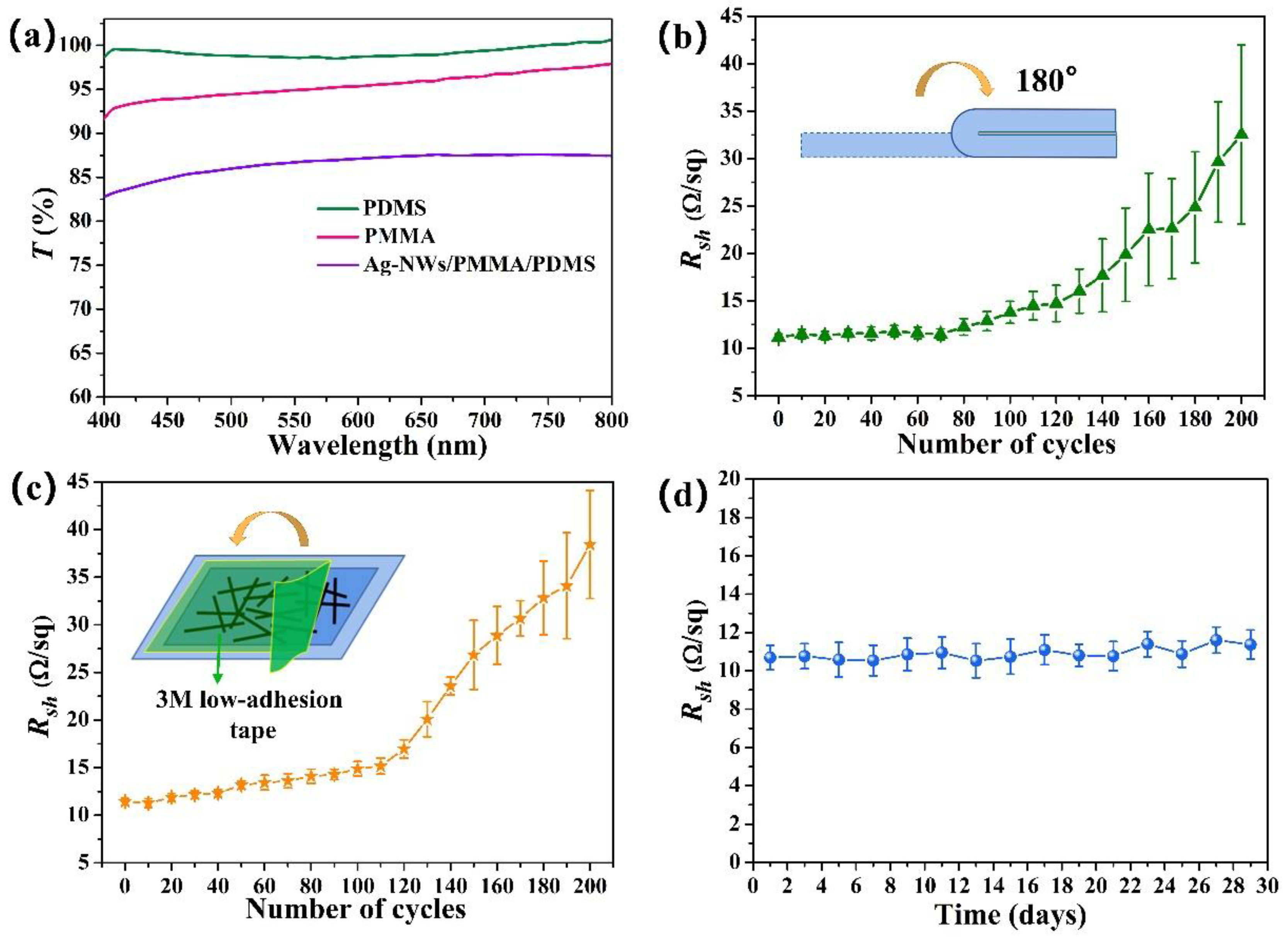
3.4. Durability of Ag-NWs/PMMA/PDMS FTEs

Figure 5a shows the transmittance spectra of PDMS, PMMA, and Ag-NWs/PMMA/PDMS FTEs in the visible band. Although the Ag-NWs slightly reduced the transmittance, the flat spectrum in the visible band indicated good transparency without wavelength selection, as shown in Figure 1c. The flexibility of Ag-NWs/PMMA/PDMS FTEs was examined by the fold-bending test. The fold-bending-induced strain (ε) was 75.6%, which was estimated by [41]
ε = t 2 R × 100 %
where t is the thickness of the FTE and R is the bending radius, which were 31.0 μm and 20.5 μm measured by the profilometer, respectively. Figure 5b shows the sheet resistance maintained for up to 100 cycles of fold-bending with high strain, and then increased due to the fatigue of Ag-NWs. In addition, the adhesion of Ag-NWs on the organic substrate was also investigated. The above-mentioned discussion indicates that the Ag-NW network was jointed onto the PMMA film during laser nano-welding, whereby the adhesion between Ag-NWs and substrate was significantly strengthened since the Ag-NWs were partially embedded in the PMMA film. The 3M low-adhesion tape was thereby used to carry out the Ag-NW adhesion test by pressing it onto the film and peeling it off. Figure 5c indicates that the sheet resistance could be kept constant for the peeling-off process for up to 110 cycles, confirming the good adhesion of Ag-NWs on the PMMA/PDMS film via laser nano-welding. Figure 5d exhibited the stability of the Ag-NWs/PMMA/PDMS FTEs in ambient atmospheric at room temperature, where the sheet resistances were constant for 1 month. The excellent durability, flexibility, adhesion, and period stability recommend the laser nano-welded Ag-NWs/PMMA/PDMS FTEs for wide application in future wearable devices.

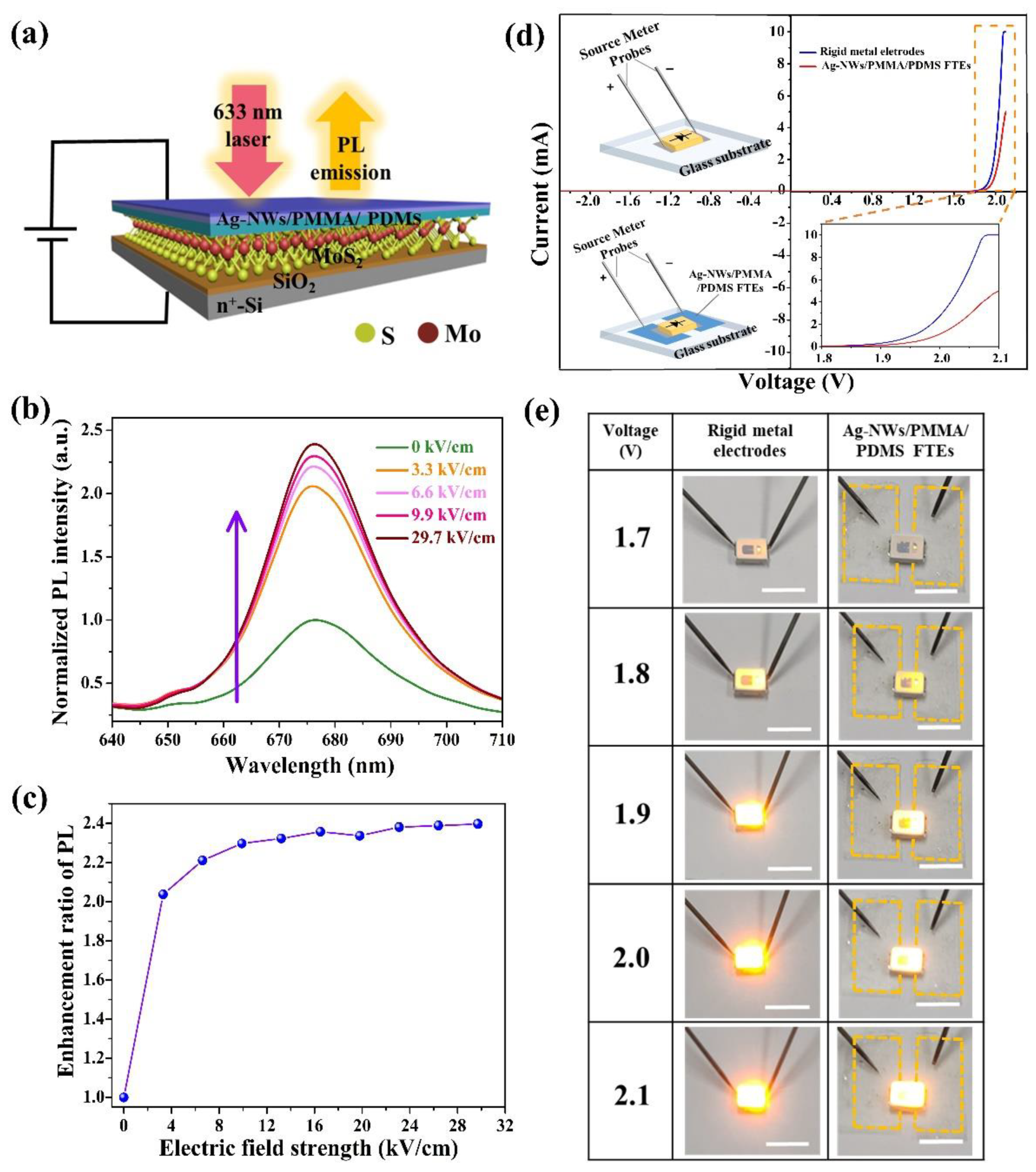
3.5. Applications of Ag-NWs/PMMA/PDMS Films as High-Performance FTEs

To demonstrate the performance of Ag-NWs/PMMA/PDMS FTEs, two typical configurations of wearable devices were employed and fabricated as shown in Figure 6. The applications of 2D materials in flexible electronic/optoelectronic components have been well-acknowledged [42]. For vertical device structures, FTEs became important for 2D material wearable designs. Figure 6a shows the typical sandwich structure for gate-controlled MoS2 luminescence, in which an Ag-NWs/PMMA/PDMS FTE covered an MoS2 monolayer, which was deposited on a 300 nm-thick SiO2 isolayer oxidized from an n+-Si substrate. The PMDS side was contacted with the MoS2 monolayer for applying the gate voltage, U, from the Ag-NW network to the n+-Si substrate. The generated electric field, E, was estimated by E = U/d, where d is the combined thickness of the PMMA, the PDMS, the MoS2 monolayer, and the SiO2 isolayer. The luminescence of the MoS2 monolayer is regulated by the gate voltage due to the interaction of excitons with charge carriers via the phase-space filling effect [43,44]. This optoelectronic property can be used to realize electro-optical modulators operating in the visible band. Owing to the high transparency and conductivity of Ag-NWs/PMMA/PDMS FTEs, the phenomenon was achieved by in-situ PL measurement, as shown in Figure 6b. The PL intensity from the MoS2 monolayer was significantly enhanced as the gate-voltage-induced electric field increased. The PL enhancement ratio was from 203.8% to 239.7% under the electric field intensity of 10.0–29.7 kV/cm, as demonstrated in Figure 6c, confirming the compatibility of Ag-NWs/PMMA/PDMS FTEs with 2D materials for electro-optical applications.
The Ag-NWs/PMMA/PDMS films can also be used as facile, high-performance conductive tapes for conventional electronic components, where the good ohmic contacts with the footprints can be achieved by van der Waals and static electrical forces instead of by soldering. Figure 6d shows the I–V characteristics of a commercial surface-mounted LED with rigid metal electrodes and FTEs, respectively. It can be clearly seen that the ohmic contacts between FTEs and LED footprints were achieved. The increased opening voltage threshold of the LED from 1.7 V to 1.8 V was attributed to the inserted resistance of the FTEs. However, the I–V curve using FTEs was very similar to that of rigid metal electrodes. The photographs of luminescence from the LEDs with various electrodes under different bias voltages are shown Figure 6e. Although the inserted resistance slightly reduced the efficiency of the LED, the luminescence behaviors suggested the superiority of FTEs over conventional metal electrodes in future flexible electronic devices.

4. Conclusions

In this work, high-performance Ag-NWs/PMMA/PDMS FTEs were fabricated by the nanosecond pulsed laser nano-welding of Ag-NWs on PMMA/PDMS flexible substrates. Compared with previous fabrication techniques, laser nano-welding provided a facile and time-saving approach to improve Ag-NW network formation and adhesion onto the flexible organic substrates. The stimulated localized surface plasmon resonances confined the incident laser energy into the cross junctions and gaps between Ag-NWs for selective melting. The Ag-NWs were therefore welded for resistance reduction and jointed with the PMMA film with high adhesive strength. The fabricated FTEs demonstrated a high transmittance of 85.9% in the visible band and a low sheet resistance of 11.3 Ω/sq, attributable to the small absorption cross section and high conductivity of the nano-welded Ag-NWs. The superior durability, high flexibility, strong adhesion, and period stability tolerance commended the FTEs for practical wearable applications, in pursuit of which two typical components in 2D material luminescence devices and LEDs were explored. The gate voltages for high electric fields for regulating the PL emission from an MoS2 monolayer was determined. The FTEs were also confirmed to be suitable for conventional electronic devices (i.e., LEDs), as a flexible-type electrode for wearable designs to replace rigid metal ones, since soldering between the FTEs and component footprints for ohmic contacts was avoided. The present work points a path forward in the development of high-performance FTEs for next-generation flexible electronic/optoelectronic devices with outstanding optical transmittance, high conductivity, and good durability.

Author Contributions

Conceptualization, Y.Y.; methodology, Y.Y. and T.W.; software, T.W. and J.H.; validation, T.W. and Y.Y.; formal analysis, T.W. and Y.Y.; investigation, T.W., Y.Y. and Y.W.; data curation, L.Z., Q.L., X.Z. (Xiaoxia Zhang), X.L., X.Z. (Xiaohua Zhang), and Y.P.; writing—original draft preparation, T.W.; writing—review and editing, Y.Y.; supervision, Y.Y. and Y.W.; project administration, Y.Y.; funding acquisition, Y.Y. All authors have read and agreed to the published version of the manuscript.

Funding

This research was funded by National Natural Science Foundation of China, grant number 12074019 and Key Program of Science and Technology Development Project of Beijing Municipal Education Commission, grant number KZ202110005002.

Data Availability Statement

The data presented in this study are available from the corresponding author.

Conflicts of Interest

The authors declare no conflict of interest.

References

  1. Chen, W.; Liu, L.X.; Zhang, H.B.; Yu, Z.Z. Flexible, Transparent, and Conductive Ti3C2Tx MXene-Silver Nanowire Films with Smart Acoustic Sensitivity for High-Performance Electromagnetic Interference Shielding. ACS Nano 2020, 14, 16643–16653. [Google Scholar] [CrossRef]
  2. Chen, X.; Xu, G.; Zeng, G.; Gu, H.; Chen, H.; Xu, H.; Yao, H.; Li, Y.; Hou, J.; Li, Y. Realizing Ultrahigh Mechanical Flexibility and >15% Efficiency of Flexible Organic Solar Cells via a “Welding” Flexible Transparent Electrode. Adv. Mater. 2020, 32, 1908478. [Google Scholar] [CrossRef]
  3. De Guzman, N.; Ramos, M., Jr.; Donnabelle Balela, M. Improvements in the electroless deposition of Ag nanowires in hot ethylene glycol for resistive touchscreen device. Mater. Res. Bull. 2018, 106, 446–454. [Google Scholar] [CrossRef]
  4. Sang, S.; Liu, L.; Jian, A.; Duan, Q.; Ji, J.; Zhang, Q.; Zhang, W. Highly sensitive wearable strain sensor based on silver nanowires and nanoparticles. Nanotechnology 2018, 29, 255202. [Google Scholar]
  5. Triambulo, R.E.; Kim, J.-H.; Park, J.-W. Highly flexible organic light-emitting diodes on patterned Ag nanowire network transparent electrodes. Org. Electron. 2019, 71, 220–226. [Google Scholar] [CrossRef]
  6. Hwang, Y.; Hwang, Y.H.; Choi, K.W.; Lee, S.; Kim, S.; Park, S.J.; Ju, B.-K. Highly stabilized flexible transparent capacitive photodetector based on silver nanowire/graphene hybrid electrodes. Sci. Rep. 2021, 11, 10499. [Google Scholar] [CrossRef]
  7. Ma, C.; Liu, H.; Teng, C.; Li, L.; Zhu, Y.; Yang, H.; Jiang, L. Wetting-Induced Fabrication of Graphene Hybrid with Conducting Polymers for High-Performance Flexible Transparent Electrodes. ACS Appl. Mater. Interfaces 2020, 12, 55372–55381. [Google Scholar] [CrossRef]
  8. Park, I.J.; Kim, T.I.; Yoon, T.; Kang, S.; Cho, H.; Cho, N.S.; Lee, J.I.; Kim, T.S.; Choi, S.Y. Flexible and Transparent Graphene Electrode Architecture with Selective Defect Decoration for Organic Light-Emitting Diodes. Adv. Funct. Mater. 2018, 28, 1704435. [Google Scholar] [CrossRef]
  9. Fang, Y.; Li, Y.; Wang, X.; Zhou, Z.; Zhang, K.; Zhou, J.; Hu, B. Cryo-Transferred Ultrathin and Stretchable Epidermal Electrodes. Small 2020, 16, 2000450. [Google Scholar] [CrossRef]
  10. Li, D.; Wang, L.; Ji, W.; Wang, H.; Yue, X.; Sun, Q.; Li, L.; Zhang, C.; Liu, J.; Lu, G.; et al. Embedding Silver Nanowires into a Hydroxypropyl Methyl Cellulose Film for Flexible Electrochromic Devices with High Electromechanical Stability. ACS Appl. Mater. Interfaces 2021, 13, 1735–1742. [Google Scholar] [CrossRef]
  11. Wang, S.; Wu, S.; Ling, Z.; Chen, H.; Lian, H.; Portier, X.; Gourbilleau, F.; Marszalek, T.; Zhu, F.; Wei, B.; et al. Mechanically and thermally stable, transparent electrodes with silver nanowires encapsulated by atomic layer deposited aluminium oxide for organic optoelectronic devices. Org. Electron. 2020, 78, 105593. [Google Scholar] [CrossRef] [Green Version]
  12. Zhang, Y.; Bai, S.; Chen, T.; Yang, H.; Guo, X. Facile preparation of flexible and highly stable graphene oxide-silver nanowire hybrid transparent conductive electrode. Mater. Res. Express 2020, 7, 016413. [Google Scholar] [CrossRef] [Green Version]
  13. Che, B.; Zhou, D.; Li, H.; He, C.; Liu, E.; Lu, X. A highly bendable transparent electrode for organic electrochromic devices. Org. Electron. 2019, 66, 86–93. [Google Scholar] [CrossRef]
  14. Jiang, S.; Hou, P.-X.; Chen, M.-L.; Wang, B.-W.; Sun, D.-M.; Tang, D.-M.; Jin, Q.; Guo, Q.-X.; Zhang, D.-D.; Du, J.-H.; et al. Ultrahigh-performance transparent conductive films of carbon-welded isolated single-wall carbon nanotubes. Sci. Adv. 2018, 4, eaap9264. [Google Scholar] [CrossRef] [Green Version]
  15. Khachatryan, H.; Kim, K.-B.; Kim, M. Fabrication of Flexible Carbon Nanotube Network on Paper Substrate: Effect of Post Treatment Temperature on Electrodes. J. Nanoelectron. Optoelecton. 2020, 15, 1442–1449. [Google Scholar] [CrossRef]
  16. Li, X.; Yu, S.; Zhao, L.; Wu, M.; Dong, H. Hybrid PEDOT:PSS to obtain high-performance Ag NW-based flexible transparent electrodes for transparent heaters. J. Mater. Sci. Mater. Electron. 2020, 31, 8106–8115. [Google Scholar] [CrossRef]
  17. Song, J.; Ma, G.; Qin, F.; Hu, L.; Luo, B.; Liu, T.; Yin, X.; Su, Z.; Zeng, Z.; Jiang, Y.; et al. High-Conductivity, Flexible and Transparent PEDOT:PSS Electrodes for High Performance Semi-Transparent Supercapacitors. Polymers 2020, 12, 450. [Google Scholar] [CrossRef] [Green Version]
  18. Yang, H.; Bai, S.; Chen, T.; Zhang, Y.; Wang, H.; Guo, X. Facile fabrication of large-scale silver nanowire-PEDOT:PSS composite flexible transparent electrodes for flexible touch panels. Mater. Res. Express 2019, 6, 086315. [Google Scholar] [CrossRef]
  19. Tan, D.; Jiang, C.; Li, Q.; Bi, S.; Song, J. Silver nanowire networks with preparations and applications: A review. J. Mater. Sci. Mater. Electron. 2020, 31, 15669–15696. [Google Scholar] [CrossRef]
  20. Park, J.; Hyun, B.G.; An, B.W.; Im, H.-G.; Park, Y.-G.; Jang, J.; Park, J.-U.; Bae, B.-S. Flexible Transparent Conductive Films with High Performance and Reliability Using Hybrid Structures of Continuous Metal Nanofiber Networks for Flexible Optoelectronics. ACS Appl. Mater. Interfaces 2017, 9, 20299–20305. [Google Scholar] [CrossRef] [PubMed]
  21. Kim, H.; Choi, S.-H.; Kim, M.; Park, J.-U.; Bae, J.; Park, J. Seed-mediated synthesis of ultra-long copper nanowires and their application as transparent conducting electrodes. Appl. Surf. Sci. 2017, 422, 731–737. [Google Scholar] [CrossRef]
  22. Ku, M.; Kim, J.; Won, J.-E.; Kang, W.; Park, Y.-G.; Park, J.; Lee, J.-H.; Cheon, J.; Lee, H.H.; Park, J.-U. Smart, soft contact lens for wireless immunosensing of cortisol. Sci. Adv. 2020, 6, eabb2891. [Google Scholar] [CrossRef]
  23. Kim, J.; Park, J.; Park, Y.-G.; Cha, E.; Ku, M.; An, H.S.; Lee, K.-P.; Huh, M.-I.; Kim, J.; Kim, T.-S.; et al. A soft and transparent contact lens for the wireless quantitative monitoring of intraocular pressure. Nat. Biomed. Eng. 2021, 5, 772–782. [Google Scholar] [CrossRef]
  24. Song, R.; Yao, S.; Liu, Y.; Wang, H.; Dong, J.; Zhu, Y.; O’Connor, B.T. Facile Approach to Fabricating Stretchable Organic Transistors with Laser-Patterned Ag Nanowire Electrodes. ACS Appl. Mater. Interfaces 2020, 12, 50675–50683. [Google Scholar] [CrossRef]
  25. Qiu, J.; Wang, X.; Ma, Y.; Yu, Z.; Li, T. Stretchable Transparent Conductive Films Based on Ag Nanowires for Flexible Circuits and Tension Sensors. ACS Appl. Nano Mater. 2021, 4, 3760–3766. [Google Scholar] [CrossRef]
  26. Giusti, G.; Langley, D.P.; Lagrange, M.; Collins, R.; Jimenez, C.; Brechet, Y.; Bellet, D. Thermal annealing effects on silver nanowire networks. Int. J. Nanotechnol. 2014, 11, 785–795. [Google Scholar] [CrossRef]
  27. Oh, J.S.; Oh, J.S.; Yeom, G.Y. Invisible Silver Nanomesh Skin Electrode via Mechanical Press Welding. Nanomaterials 2020, 10, 633. [Google Scholar] [CrossRef] [PubMed] [Green Version]
  28. Liu, Y.; Zhang, J.; Gao, H.; Wang, Y.; Liu, Q.; Huang, S.; Guo, C.F.; Ren, Z. Capillary-Force-Induced Cold Welding in Silver-Nanowire-Based Flexible Transparent Electrodes. Nano Lett. 2017, 17, 1090–1096. [Google Scholar] [CrossRef]
  29. Yan, X.; Li, X.; Zhou, L.; Chu, X.; Yang, F.; Chi, Y.; Yang, X. Electrically sintered silver nanowire networks for use as transparent electrodes and heaters. Mater. Res. Express 2019, 6, 116316. [Google Scholar] [CrossRef]
  30. Hong, C.H.; Oh, S.K.; Kim, T.K.; Cha, Y.J.; Kwak, J.S.; Shin, J.H.; Ju, B.K.; Cheong, W.S. Electron beam irradiated silver nanowires for a highly transparent heater. Sci. Rep. 2015, 5, 17716. [Google Scholar] [CrossRef] [Green Version]
  31. Liang, X.; Lu, J.; Zhao, T.; Yu, X.; Jiang, Q.; Hu, Y.; Zhu, P.; Sun, R.; Wong, C.-P. Facile and Efficient Welding of Silver Nanowires Based on UVA-Induced Nanoscale Photothermal Process for Roll-to-Roll Manufacturing of High-Performance Transparent Conducting Films. Adv. Mater. Interfaces 2019, 6, 1801635. [Google Scholar] [CrossRef]
  32. Hu, Y.; Liang, C.; Sun, X.; Zheng, J.; Duan, J.A.; Zhuang, X. Enhancement of the Conductivity and Uniformity of Silver Nanowire Flexible Transparent Conductive Films by Femtosecond Laser-Induced Nanowelding. Nanomaterials 2019, 9, 673. [Google Scholar] [CrossRef] [PubMed] [Green Version]
  33. Lee, P.; Kwon, J.; Lee, J.; Lee, H.; Suh, Y.D.; Hong, S.; Yeo, J. Rapid and Effective Electrical Conductivity Improvement of the Ag NW-Based Conductor by Using the Laser-Induced Nano-Welding Process. Micromachines 2017, 8, 164. [Google Scholar] [CrossRef] [Green Version]
  34. Liu, L.; Peng, P.; Hu, A.; Zou, G.; Duley, W.W.; Zhou, Y.N. Highly localized heat generation by femtosecond laser induced plasmon excitation in Ag nanowires. Appl. Phys. Lett. 2013, 102, 073107. [Google Scholar] [CrossRef] [Green Version]
  35. Nian, Q.; Saei, M.; Xu, Y.; Sabyasachi, G.; Deng, B.; Chen, Y.P.; Cheng, G.J. Crystalline Nanojoining Silver Nanowire Percolated Networks on Flexible Substrate. ACS Nano 2015, 9, 10018–10031. [Google Scholar] [CrossRef]
  36. Bell, A.R.; Fairfield, J.A.; McCarthy, E.K.; Mills, S.; Boland, J.J.; Baffou, G.; McCloskey, D. Quantitative Study of the Photothermal Properties of Metallic Nanowire Networks. ACS Nano 2015, 9, 5551–5558. [Google Scholar] [CrossRef]
  37. Kang, T.; Yoon, I.; Jeon, K.-S.; Choi, W.; Lee, Y.; Seo, K.; Yoo, Y.; Park, Q.H.; Ihee, H.; Suh, Y.D.; et al. Creating Well-Defined Hot Spots for Surface-Enhanced Raman Scattering by Single-Crystalline Noble Metal Nanowire Pairs. J. Phys. Chem. C 2009, 113, 7492–7496. [Google Scholar] [CrossRef] [Green Version]
  38. Prokes, S.M.; Alexson, D.A.; Glembocki, O.J.; Park, H.D.; Rendell, R.W. Effect of crossing geometry on the plasmonic behavior of dielectric core/metal sheath nanowires. Appl. Phys. Lett. 2009, 94, 093105. [Google Scholar] [CrossRef] [Green Version]
  39. Lei, D.Y.; Aubry, A.; Maier, S.A.; Pendry, J.B. Broadband nano-focusing of light using kissing nanowires. New J. Phys. 2010, 12, 093030. [Google Scholar] [CrossRef]
  40. Haacke, G. New figure of merit for transparent conductors. J. Appl. Phys. 1976, 47, 4086–4089. [Google Scholar] [CrossRef]
  41. Park, Y.-G.; Kim, H.; Park, S.-Y.; Kim, J.-Y.; Park, J.-U. Instantaneous and Repeatable Self-Healing of Fully Metallic Electrodes at Ambient Conditions. ACS Appl. Mater. Interfaces 2019, 11, 41497–41505. [Google Scholar] [CrossRef]
  42. Samy, O.; Zeng, S.; Birowosuto, M.D.; El Moutaouakil, A. A Review on MoS2 Properties, Synthesis, Sensing Applications and Challenges. Crystals 2021, 11, 355. [Google Scholar] [CrossRef]
  43. Newaz, A.K.M.; Prasai, D.; Ziegler, J.I.; Caudel, D.; Robinson, S.; Haglund, R.F., Jr.; Bolotin, K.I. Electrical control of optical properties of monolayer MoS2. Solid State Commun. 2013, 155, 49–52. [Google Scholar] [CrossRef] [Green Version]
  44. Yi, H.T.; Rangan, S.; Tang, B.; Frisbie, C.D.; Bartynski, R.A.; Gartstein, Y.N.; Podzorov, V. Electric-field effect on photoluminescence of lead-halide perovskites. Mater. Today 2019, 28, 31–39. [Google Scholar] [CrossRef]
Figure 1. Fabrication of Ag-NWs/PMMA/PDMS FTEs. (a) Schematic of synthesis procedure. (b) Cross-section schematic of the FTEs. (c) Mechanical and optical properties of the FTEs.
Crystals 11 00996 g001
Figure 2. Morphologies and electrical properties of Ag-NWs/PMMA/PMMA FTEs via ns-pulsed laser nano-welding under various process parameters. (a) SEM images. (b) Close-up view of as-deposited Ag-NWs before nano-welding. (cf) Laser nano-welding of Ag-NWs under laser fluence of (c) 10.0 mJ/cm2, (d) 17.4 mJ/cm2, (e) 27.9 mJ/cm2, and (f) 37.9 mJ/cm2 at irradiation time of 50 s. (g,h) TEM images of (g) as-deposited and (h) laser nano-welded Ag-NWs. (i) Evolution of sheet resistance with laser fluence and irradiation time.
Crystals 11 00996 g002
Figure 3. Numerical simulation of laser nano-welding of Ag-NWs and validation of Ag-NWs jointing with PMMA substrates. (a) Cross junction. (b) Head-to-head configurations for simulation. (c,d) Electric field distributions and intensities (c) near the cross junction between Ag-NWs and (d) near the gap of head-to-head Ag-NWs. (e,f) Removal experiments using 3M low-adhesion tapes for (e) as-deposited and (f) laser nano-welded Ag-NWs on PMMA film.
Crystals 11 00996 g003
Figure 4. Evolution of transmittance and sheet resistance of Ag-NWs/PMMA/PDMS FTEs with the number of spraying layers using Ag-NW suspension concentrations of (a) 0.3 mg/mL, (b) 0.4 mg/mL, (c) 0.5 mg/mL, (d) 0.6 mg/mL, and (e) 0.7 mg/mL, as well as the calculated FoMs. (f) Optimization from various suspension concentration and spraying layer parameter sets.
Crystals 11 00996 g004
Figure 5. Durability of Ag-NWs/PMMA/PDMS FTEs. (a) Transmittance spectra in the visible band. (bd) Durability tests for (b) flexibility, (c) adhesion, and (d) period stability.
Crystals 11 00996 g005
Figure 6. Applications of Ag-NWs/PMMA/PDMS FTEs. (a) Sandwich structure for gate-controlled PL emission from MoS2 monolayer. (b) PL spectra of MoS2 monolayer under various gate-voltage-induced electric field strengths. (c) Evaluation of PL enhancement ratio with electric field strength. (d) I–V curves of commercial LEDs with rigid metal electrodes and FTEs, where the insets demonstrate the experimental setups. (e) Photographs of luminescence from the LEDs under various bias voltages through different electrodes.
Crystals 11 00996 g006
Publisher’s Note: MDPI stays neutral with regard to jurisdictional claims in published maps and institutional affiliations.

