Article

Ultra-Fast Laser Fabrication of Alumina Micro-Sample Array and High-Throughput Characterization of Microstructure and Hardness

1
Department of Materials Science and Engineering, Clemson University, Clemson, SC 29634, USA
2
Department of Electrical and Computer Engineering, Clemson University, Clemson, SC 29634, USA
3
Center for Optical Materials Science and Engineering Technologies (COMSET), Clemson University, Anderson, SC 29625, USA
4
Advanced Manufacturing LLC, East Hartford, CT 06108, USA
*
Authors to whom correspondence should be addressed.
Crystals 2021, 11(8), 890; https://doi.org/10.3390/cryst11080890
Submission received: 31 May 2021 / Revised: 17 July 2021 / Accepted: 29 July 2021 / Published: 30 July 2021
(This article belongs to the Special Issue Grain Size Control in the Processing of Poly-Crystalline Materials)

Abstract

:
In the light of recent advances in material informatics, there is a great demand for high-throughput approaches of sample fabrication and property characterization. Currently, no high-throughput approach has been demonstrated for the fast sampling of the microstructure and the correlated properties. In this paper, we demonstrate the ultra-fast fabrication of an alumina sample array and the high-throughput hardness characterization of these sample units. The alumina sample array was fabricated using picosecond (PS) laser micromachining and CO2 laser sintering within a short time (i.e., less than a few minutes). After laser sintering, the hardness of these sample units was characterized using micro-indentation, and the microstructure was observed using scanning electron microscopy (SEM). In each sample unit, the microstructure was uniform for the entire top surface and within about 20 µm depth from the top surface. The relative density (RD) and corresponding micro-hardness of the sample units was found to continuously vary over a wide range from 89% RD with 600 kgf/mm2 hardness to 99% RD with 1609 kgf/mm2 hardness. For these laser-sintered samples, the correlation of hardness and relative density of the alumina matched well with the literature reports on sintered alumina obtained using conventional low-throughput furnace sintering experiments.

1. Introduction

The correlation between microstructure and properties of ceramics has been studied for years. This is because the microstructure has a strong and deterministic effect on certain material properties [1,2,3]. For example, the grain size distribution strongly affects the conductivity of ceramic electrolyte [4,5,6] and the hardness of ceramics [7,8]. The porosity is an important factor that affects the elastic properties and hardness of ceramics [9,10] and the catalytical performance and conductivity of ceramic electrodes [11,12].
Recently, machine learning (ML)-guided materials design and prediction has attracted great attention [13,14,15,16,17,18,19,20,21,22]. For example, in our previous study, we demonstrate an ML algorithm that can predict alumina’s microstructure based on the input of processing parameters [23]. One of the greatest challenges in the ML-guided materials design and prediction is the lack of consistent material’s databases that contain a large quantity of data for ML training. Normally, ceramic samples are sintered in a furnace under a predetermined thermal cycle. The complete heat treatment, including heating up, isothermal soaking, and cooling down, takes several hours. Typically, each heat treatment cycle results in one unique data point in terms of the microstructure. If we want to explore a wide range of microstructures and the resultant properties, conventional furnace heat treatment is inefficient.
To effectively establish a material’s database, high-throughput sample fabrication and characterization are desired. Many previous high-throughput ceramic sample fabrication methods have been demonstrated based on the combinatorial methods [24,25,26,27]. In these studies, the focus was to vary the compositions, not the microstructures, of the samples in a sample array. The sample array was typically sintered in a furnace that would take many hours. Typically, these high-throughput studies are focused on the materials whose properties are sensitive to the compositions, e.g., piezoelectric ceramics [24,25].
A high-throughput method that focuses on fast sampling in the space of microstructure has not yet been demonstrated. In our previous study, we reported the ultra-fast, selective laser sintering of alumina [28]. Due to the Gaussian distribution of the laser beam intensity, the laser-sintered alumina had a highly heterogeneous microstructure depending on the position of alumina relative to the laser beam [28]. At the center of the laser beam track, the material was sintered to a high density, and away from the center, the alumina was sintered to a relatively low density. Using this important observation of Ref. [28], in this paper, we demonstrate an experimental approach that fabricates an alumina sample array with a broad range of microstructures through picosecond (PS) laser micromachining and CO2 laser sintering. With this approach, hundreds of samples can be quickly heat treated (i.e., within about one minute). After laser sintering, the hardness and microstructure of each sample unit were characterized using micro-indentation and scanning electron microscopy (SEM). We can effectively establish a database of a wide range of microstructures from ~80 samples and their corresponding hardness. Due to the strong correlation between the hardness and the relative density of alumina [29,30], we characterized the relative densities of the laser-sintered alumina, based on the SEM micrographs. The correlation between the hardness and relative density agrees well with the literature. This validates our high-throughput approach of establishing the database of hardness and microstructure for laser-sintered alumina.

2. Materials and Methods

2.1. Green Alumina Paste Casting

Alumina paste was prepared by mixing 79.75 wt.% Al2O3 powder (Almatis A152SG, d50 = 1.2 μm, Purity: 99.8%, with 0.07% MgO as the sintering aid, the rest of the impurities are: 0.04% SiO2, 0.06% Na2O, 0.02% Fe2O3, and 0.05% CaO) with 0.1 wt.% dispersant (Darvan 821A) and 20.0 wt.% DI water. The suspension was ball milled for 48 h, and 0.15 wt.% binder (hydroxypropyl) methyl cellulose (HPMC) was added slowly. Finally, the mixture was mechanically blended in vacuum for 1 h to obtain the alumina paste. The alumina paste was deposited on a silica substrate with ~500 µm thickness, using a doctor blade. The deposited alumina paste was dried at room temperature in air for 24 h to create the green tape.

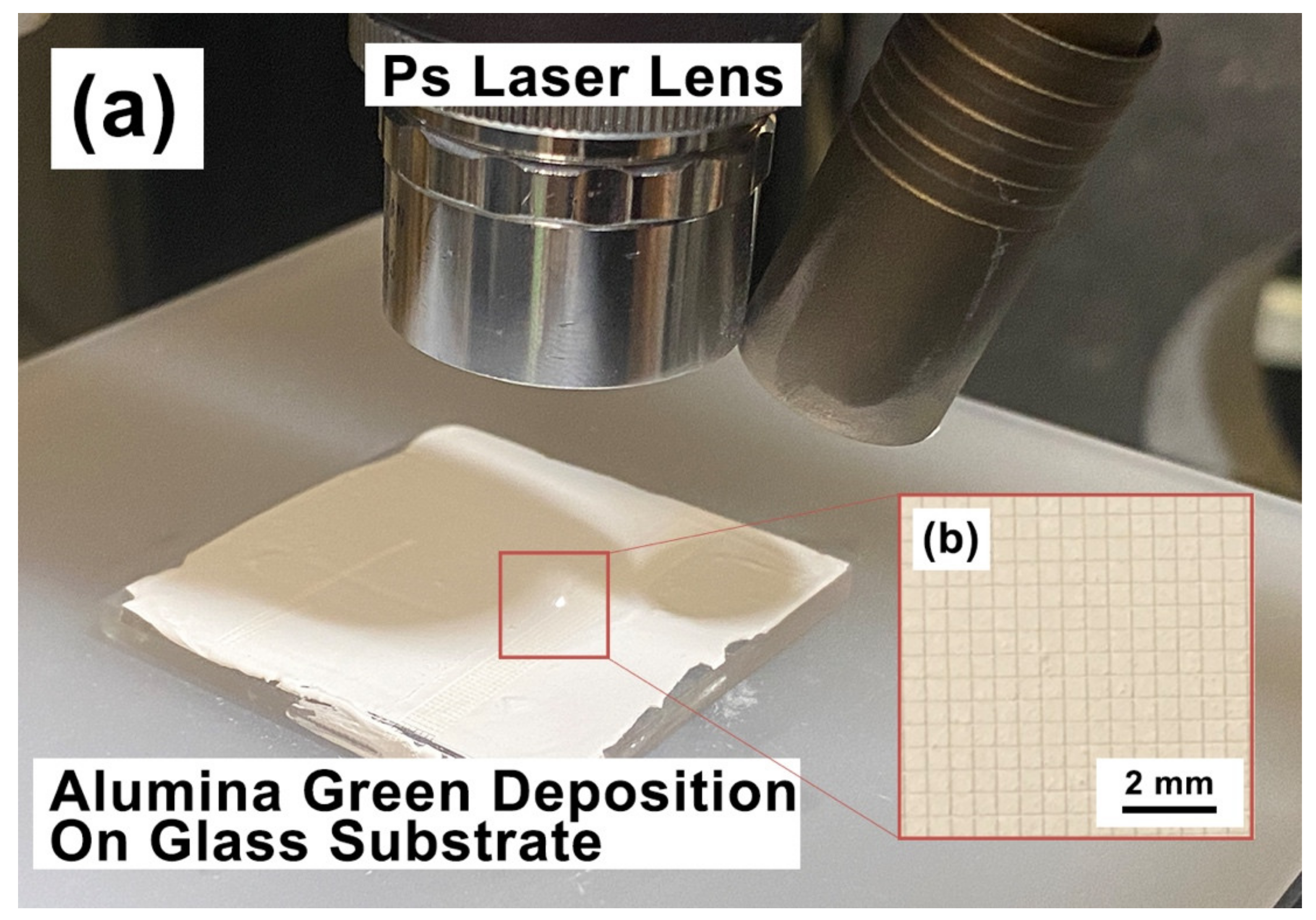
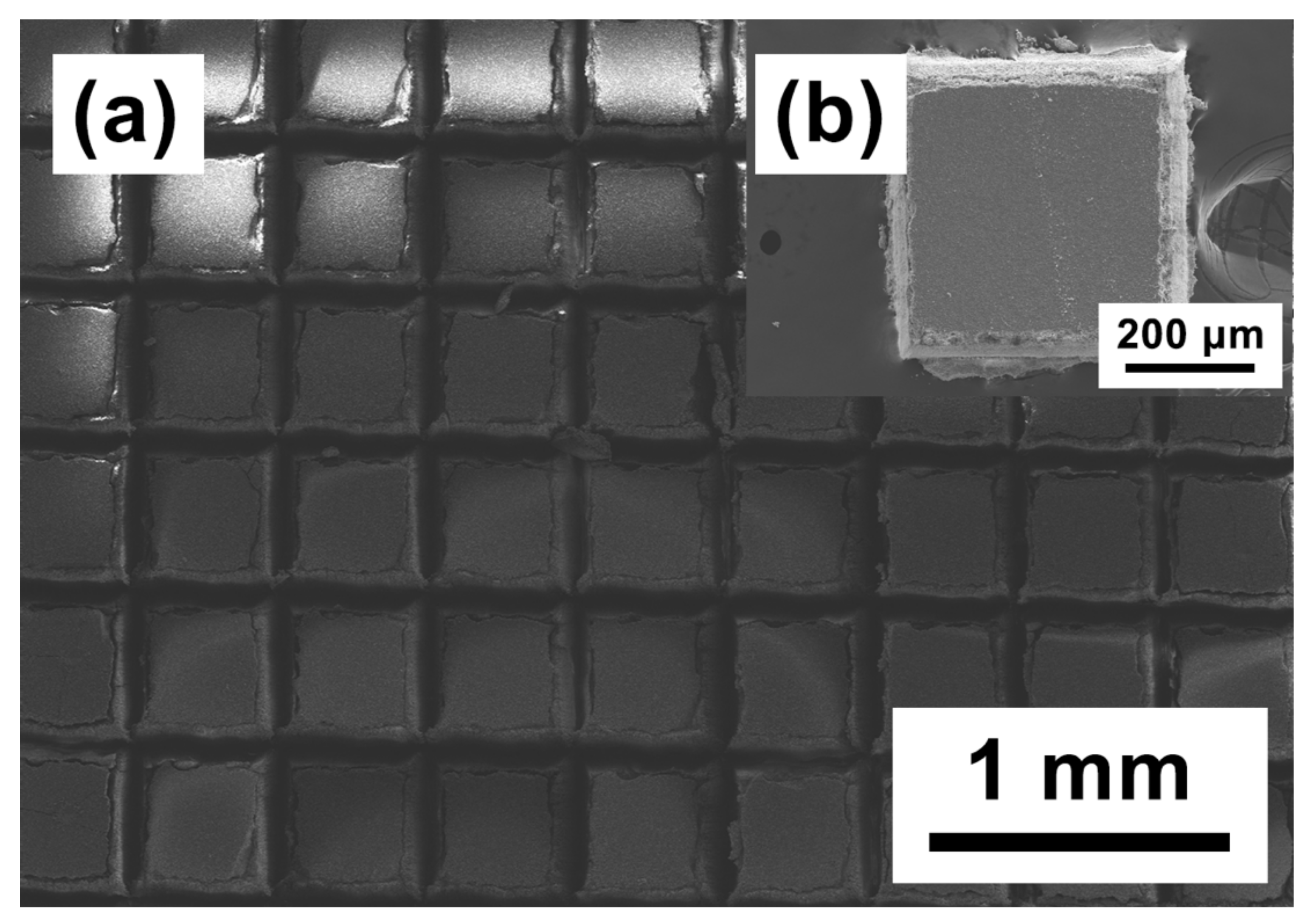
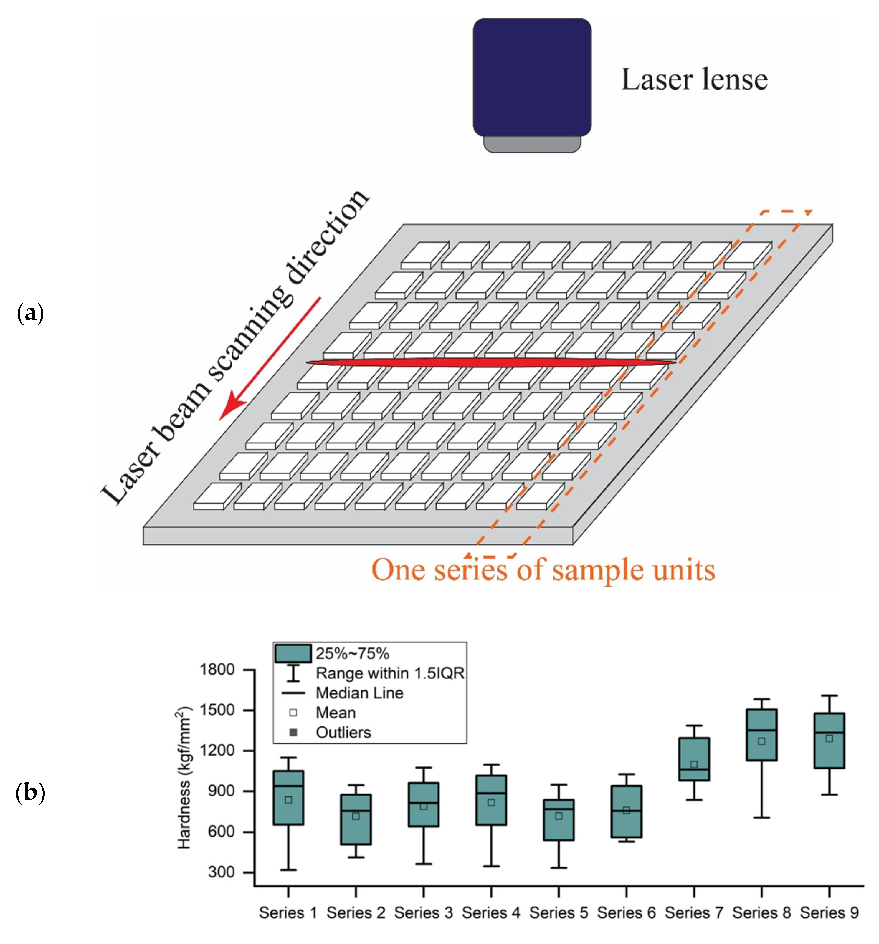
2.2. High-Throughput Ceramic Sample Fabrication

A Picosecond Laser (PXxxx-1, wavelength 1048 µm, EdgeWave, Inc., San Diego, CA, USA) was used to micromachine the green alumina deposition into square arrays with each unit of 450 µm × 450 µm size, shown in Figure 1. The repetition rate was set to 10 kHz, laser energy was 1.35 W, and the scanning speed was 5 mm/s. The PS laser setup was the same as the setup in our previous paper [31]. In order to cut through the alumina green tape, the PS laser scanning was repeated five times. The laser micro-cutting penetrated the entire depth of alumina pastes, such that the alumina sample units were not touching each other.
This micro-machined green alumna sample array was scanned using a CO2 laser (Firestar v20, wavelength 10.6 μm, SYNRAD, Inc., Mukilteo, WA, USA), with a cylindrical lens (focal length = 1 inch, diameter 19.05 mm, Laser Mechanisms, Inc., Novi, MA, USA). The cylindrical lens resulted in a line-shaped laser beam, such that the width of the laser beam (~8 mm long) covered the entire area of the sample array when the laser scanned along the sample length of the array. The laser power was 64.5 W, and the laser scanning rate was 0.1 mm/s. These parameters were the same as those used in Ref. [28], where they were presented in detail. These parameters were shown to result in desired sintering behavior for alumina. Using this method, about one hundred alumina samples were sintered in one experiment with laser scanning. The low magnification SEM of the sample array is shown in Figure 2. After sintering, top surface of each sample was ~400 µm × 400 µm.
The absorptivity of alumina for the PS laser at a wavelength of 1064 nm is 3%, and for the CO2 laser at a wavelength of 10.6 µm, it is 96% [32]. Although, alumina has low absorptivity for the PS laser, the micromachining of alumina paste using the PS laser can be well controlled, as discussed in our previous paper [31]. This is probably because the alumina paste was not sintered and was only powder compact when PS laser micromachining was conducted. Due to the good absorptivity at the CO2 laser wavelength, the alumina was sintered quite effectively

2.3. Hardness and Microstructure Characterization

The microstructure was characterized using the SEM (Hitachi S4800, Hitachi, Ltd., Tokyo, Japan and Hitachi S6600, Hitachi, Ltd., Tokyo, Japan). The microhardness of laser-sintered alumina arrays was characterized using a microhardness tester (MHT-210 micro hardness tester, LECO Corporation, St. Joseph, MI, USA). Vickers indentation was introduced on the sample surface, and its size was measured on SEM-generated micrographs. A typical micro-indentation is shown in Figure 3.
According to the definition of hardness and geometry of Vickers indentation, the Vickers hardness can be calculated as [33]:
H V =   F A 1.8544 F d 2  
where HV is Vickers hardness in kgf/mm2 [34], F is the applied force in kgf, A is the surface area of the resulting indentation in square millimeters, and d is the average length of the diagonal left by the indenter in millimeters. The applied force and loading time were set as 500 gf for 30 s.
Three indentation measurements were carried out for each sample unit. The hardness value of a sample unit was the average of the three measurements. Normally these three measurements were very close to each other (within 5% error). For rare cases, there was a failed indentation on one sample unit. For example, there was a crack in the indent and the measurement was not accurate. Then, the reported hardness for that sample unit was calculated based on the two successful measurements.
The detailed procedure of analyzing SEM micrographs to obtain the relative density of laser-sintered alumina is presented in our previous work [28]. Briefly, to calculate the relative density of each laser-sintered alumina sample, the pore area in the SEM image of the given microstructure was darkened and then analyzed using image processing software (ImageJ from NIH [35]). The SEM-based relative density was then calibrated with the Archimedes density on furnace-sintered alumina samples.

3. Results and Discussion

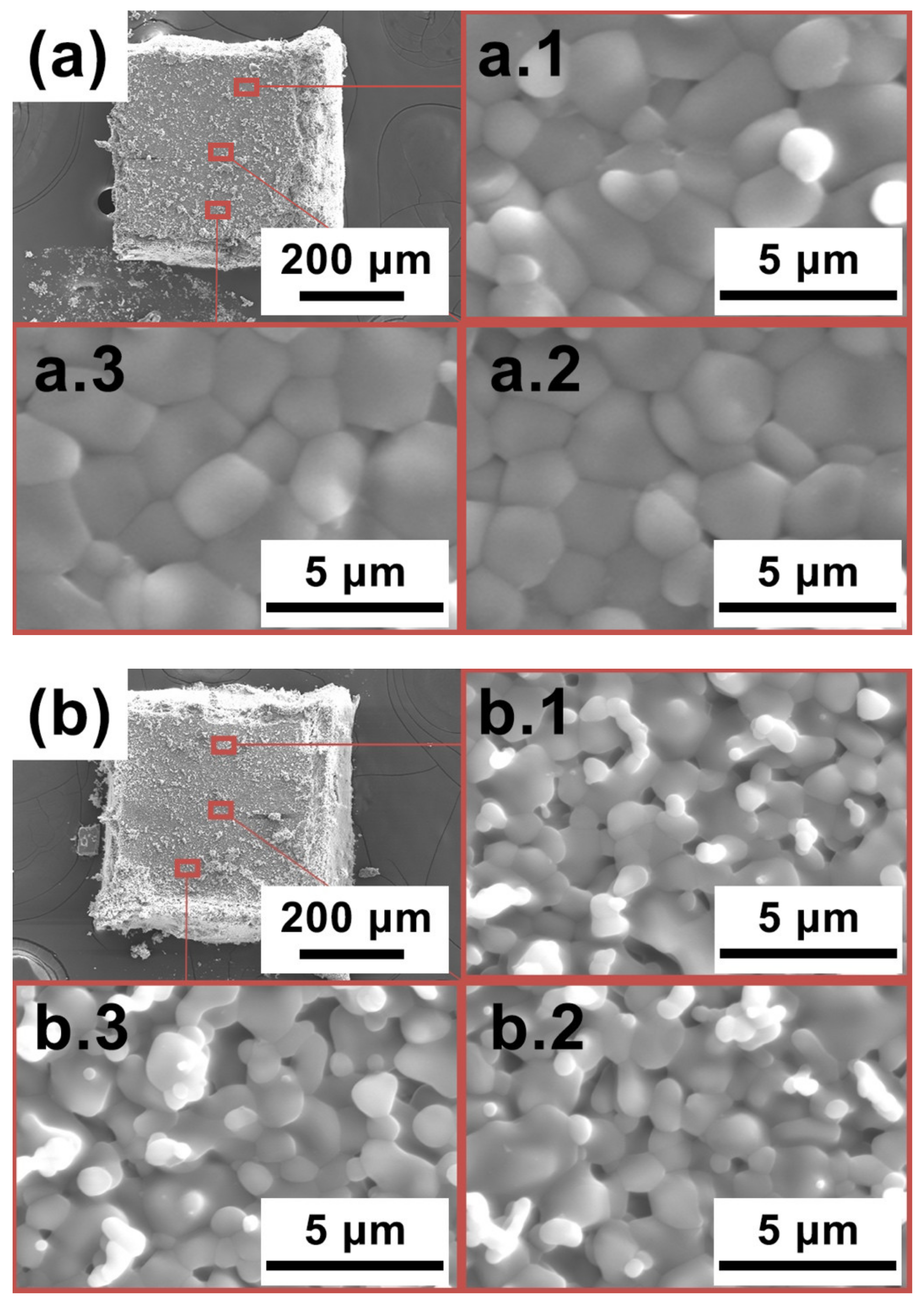
3.1. Microstructure Uniformity of Micro-Sample Units

After laser sintering, different microstructures were obtained for different sample units in the array. As shown in Figure 4, high and low relative densities were observed for different units. We examined different locations within sample units from the top-view, and found that within one sample unit, the microstructure is always uniform, in terms of grain size and relative density. As shown in Figure 4, we randomly picked three different locations in a sample unit and observed with high-magnification SEM. Typically, one location was in the center of the sample unit (e.g., Figure 4(a.2,b.2)) and the other two were close to the different sides of the unit (e.g., Figure 4(a.1,a.3,b.1,b.3)). For all the sample units we observed, no matter the relative density low or high, all these three locations had similar grain morphologies, grain sizes, and porosities. In summary, the surface microstructure of laser-sintered alumina sample units was different between units but the same within the unit.
The microstructure uniformity along the depth direction was also examined. We observed the cross-section view of the sample units, as shown in Figure 5. The microstructure of the sample units was not homogeneous along the Z-direction. This is typical for the laser sintering of alumina since most of the laser power was absorbed on the top surface, leading to a temperature gradient along the Z-direction (thickness). Compared to the bottom part of the alumina sample unit, the top surface part had a larger grain size and a higher relative density.
However, we examined the cross-sections of the sample units and found that within at least 20 µm from the top surface, the microstructure was uniform, as shown in similar relative density according to the Figure 5a,b. Considering the geometry of Vickers indenter, the depth of indentation, t, can be calculated as [36]:
t = d 2 2 t a n θ 2 d 7.0006    
where d is the average length of the diagonal left by the indenter and θ is the included angle between plane faces of the indenter tip. Here, 136° was used for Vickers indenter. Using the typical Vickers indentation diameter from Figure 3 (around 35 µm) and using Equation (2), the typical indentation depth is calculated to be ~5 µm), which is much smaller than 20 µm (the estimated depth of uniform microstructure). Although the overall cross-section had a nonuniform microstructure, the top zone, probed by the Vickers indenter, had a uniform microstructure that ensures that each hardness measurement is on samples with uniform microstructures.

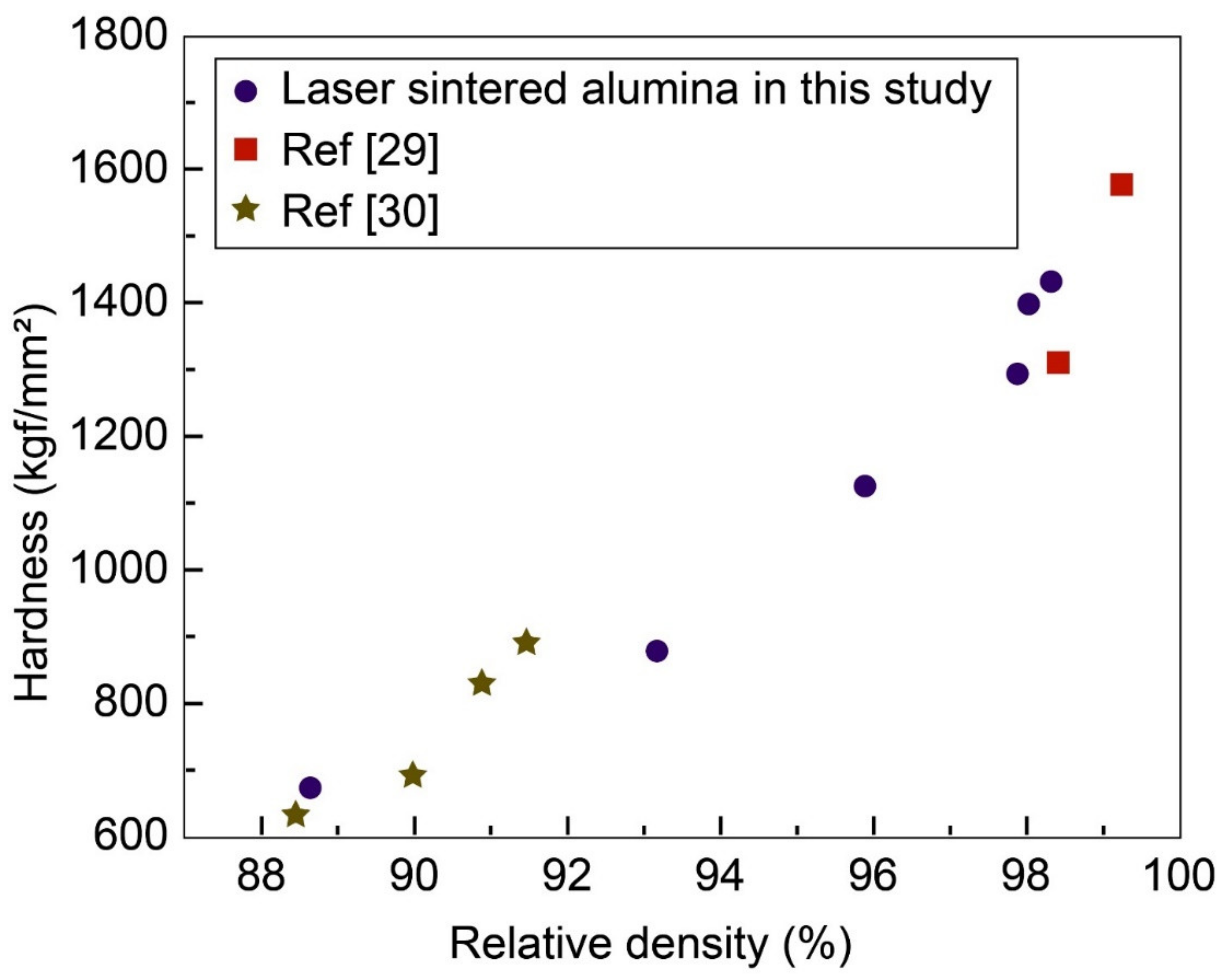
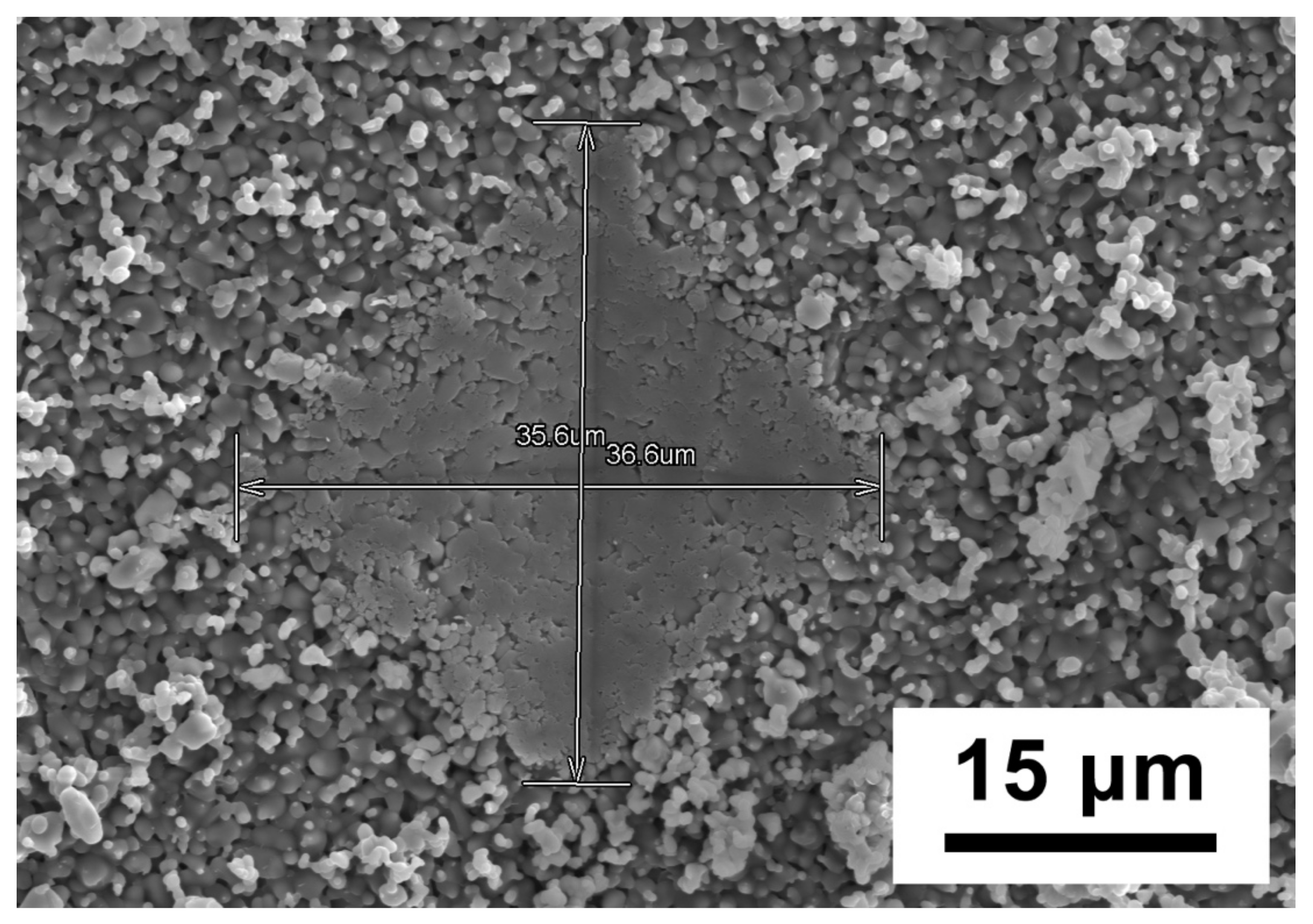
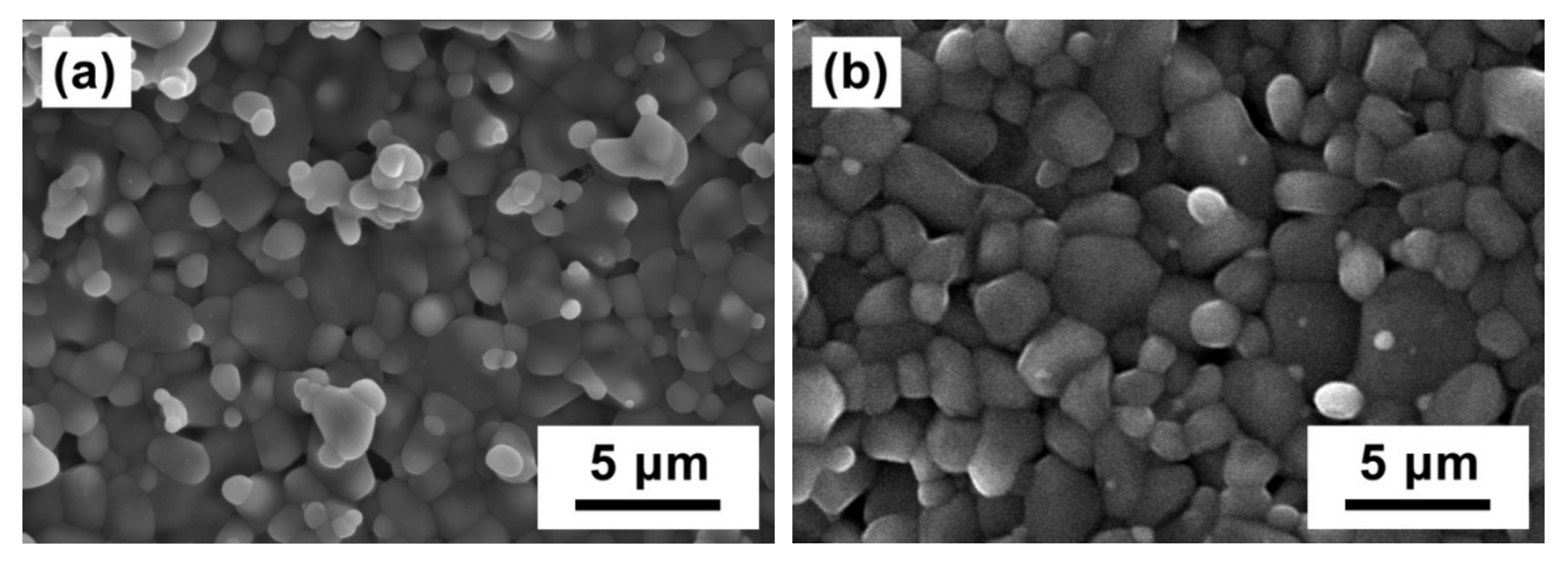
3.2. Distributions of Microhardness and the Corresponding Microstructure

The micro-indentation can be carried out for all the sample units. Since each sample unit is about 400 µm × 400 µm, and the size of the indent is about 40 µm along the diagonal direction, we took three independent indents on each sample unit. Then, the sizes of the indents of all the sample units were characterized under SEM.
As shown in Figure 6, along the laser scanning direction, we expect the microstructure, and the corresponding microhardness of the sample units are close, because these samples were irradiated under the similar laser power intensity. We group the sample units along the laser scanning direction as one series of samples. Each series contains nine individual units. As shown in Figure 6b, statistically the hardness varied between series. For example, Series 8 and 9 had an average hardness above 1200 kgf/mm2, while Series 2 and 6 had an average hardness below 900 kgf/mm2.
The laser power and scanning speed were kept constant during sintering. Under ideal conditions, the constant processing parameters would imply that the hardness of sample units in each of these series would be constant. However, as can be seen from Figure 6b, this is not the case. We believe that this is due to the inherent fluctuation of laser power and the difference between the boundary conditions of each sample unit. This is the reason that we need to correlate the hardness with microstructure, and not the locations of the sample in this study. This has been done in the following sections.

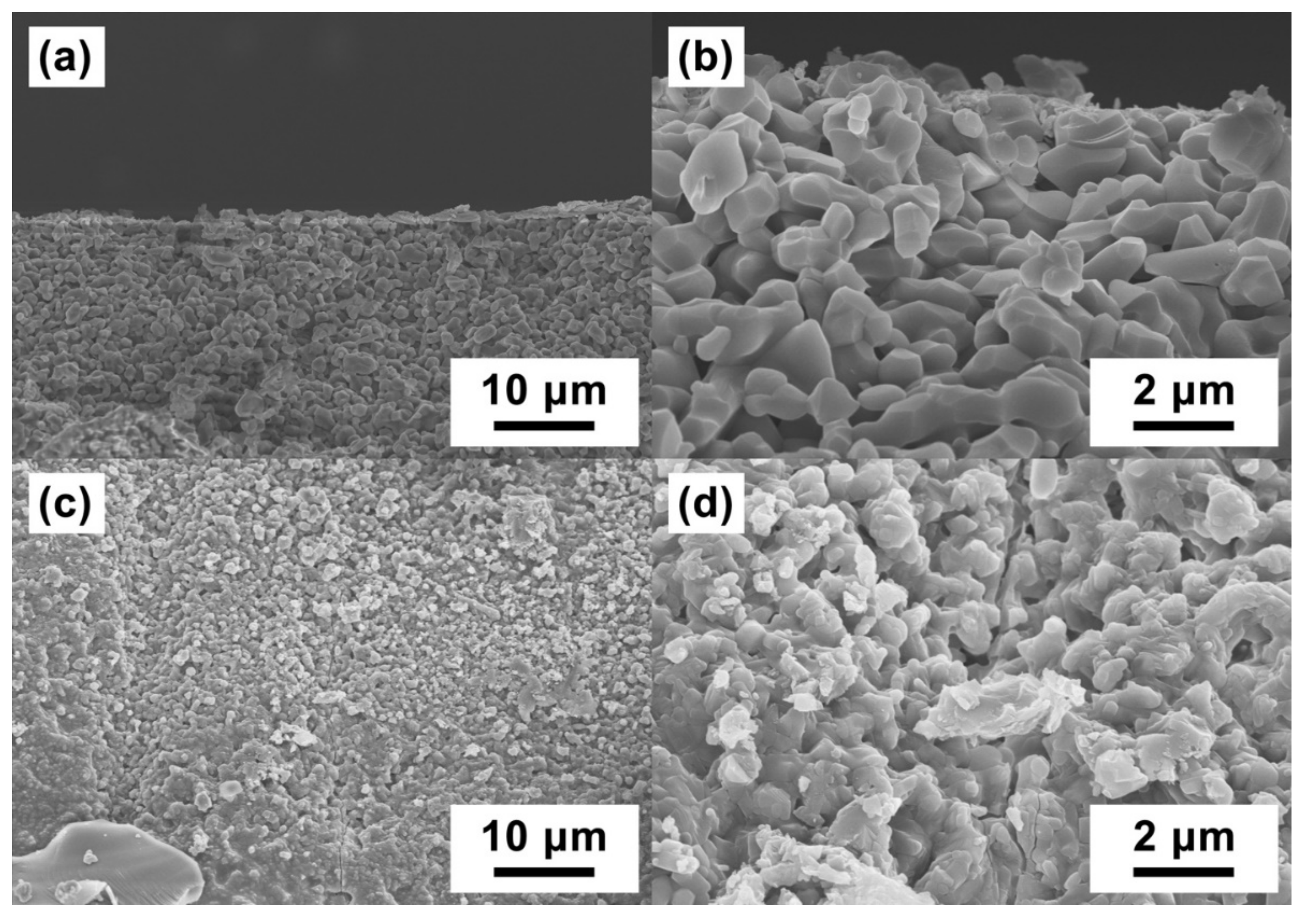
3.3. Quantitative Characterization of Relative Density from SEM Micrographs

The hardness of sintered alumina is strongly influenced by the microstructure features, such grain size and especially relative density [7,8,29,30]. Studies show that higher relative density corresponds to higher hardness [29,30].
The challenge to quantitatively characterize the relative density of laser-sintered alumina is that each sample unit is very small (i.e., ~400 µm × 400 µm), and the microstructural uniform region is limited to a depth of ~20 µm from the top surface. Therefore, we cannot use the Archimedes method to measure the relative density. To quantitatively characterize the relative density from SEM micrographs, we developed a benchmarking method [28]. In this method, the pore areal fraction of the SEM from laser-sintered alumina is compared with that from the furnace-sintered alumina. When the two fractions match, we consider the laser-sintered alumina to have the same relative density as furnace-sintered alumina. The relative density of furnace-sintered alumina can be characterized using Archimedes’ method. For example, as shown in Figure 7, the laser-sintered alumina has the same relative density as furnace-sintered alumina (relative density = 98%). Ideally, a polished surface should be used to characterize the microstructure features. However, the homogeneous layer of the laser-sintered layer was very thin (~20 µm). This part of the sample would be very easily ground off during polishing.

3.4. High-Throughput Database of Hardness and Corresponding Microstructure

We rearranged the samples’ indices based on their hardness from low to high. Then, all the hardness results above 600 kgf/mm2 can be rearranged from the lowest to the largest, as shown in Figure 8. The hardness of the microsamples continuously varied from 600 to 1609 kgf/mm2. A wide range of hardness values were represented in these sample units. Correspondingly, these samples also demonstrated continuously varying, vastly different microstructures. The relative densities of the micro sample units continuously varied from 88% to ~100%.
The correlation between the hardness and relative density of high-throughput samples is shown in Figure 9. Hardness increased monotonically with the increase in the relative density. The data points also agree well with the literature [29,30]. Since calculating relative density from SEM micrographs is time consuming, we did not plot all the relative densities from the sample array in Figure 9. In the future, ML algorithms will be developed to predict the microstructure from the hardness values, similar to our previous work [23]. Since the hardness measurement is much faster than microstructural characterization, we can conveniently predict the material’s microstructure based on the hardness measurement.
The hardness-relative density correlation, shown in Figure 9, was not solely caused by the relative density, but a combined effect of relative density and grain size. However, the relative density is the dominant factor for the density range investigated in this paper. In the literature, grain size has also been shown to be an important microstructural variable that controls the hardness, especially for the fully dense alumina. For example, a previous study found that submicrometer alumina had much higher hardness than the micrometer grain-sized alumina, when the density was about the same (99.2 ± 0.4%) [37]. In general, the smaller grain size correlates to the higher hardness for sintered alumina. In laser-sintered alumina, there is a direct correlation between the grain size and density, as reported in our previous study [28]. A larger relative density corresponds to larger grain sizes. If the grain size were the dominate factor, we would have observed lower hardness for a higher relative density.

4. Conclusions

In this paper, we reported a novel approach for high-throughput alumina sample fabrication and characterization. Using PS laser prior micromachining and CO2 laser sintering, an alumina sample array was obtained that contained ~80 small sample units of 400 µm × 400 µm size. The laser fabrication was very fast (e.g., <1 min) compared to the conventional furnace sintering (e.g., hours to days). Due to the heterogenous temperature distribution during laser sintering, the microstructure and hardness of the sample units varied greatly. For each individual sample unit, the microstructure was uniform over the entire top surface and within about 20 µm depth from the top surface. Three micro-indentation measurements were carried out for each sample unit. The hardness of the sample units continuously varied from 600 to 1609 kgf/mm2, with a relative density ranging from 88% to nearly 100%. The hardness of each units showed a strong correlation with their relative density. This microstructure–hardness correlation matches the literature reports quite well. The database of the microstructure and hardness of laser-sintered alumina can be efficiently established through this high-throughput laser sintering approach.

Author Contributions

Conceptualization, F.P., R.K.B. and D.L.; methodology, X.G., B.S., S.S.; validation, J.T. (Jianan Tang); formal analysis, X.G.; investigation, F.P., R.K.B. and D.L.; resources, H.X.; data curation, X.G.; writing—original draft preparation, X.G. and F.P.; writing—review and editing, R.K.B.; visualization, X.G.; supervision, F.P.; project administration, F.P.; funding acquisition, H.X. and J.T. (Jianhua Tong). All authors have read and agreed to the published version of the manuscript.

Funding

This research was funded by DOE/NETL (DE-FE0031826) and DOE/EERE (DE-EE0008428).

Conflicts of Interest

The authors declare no conflict of interest. The funders had no role in the design of the study; in the collection, analyses, or interpretation of data; in the writing of the manuscript, or in the decision to publish the results.

References

  1. Cook, R.F.; Lawn, B.R.; Fairbanks, C.J. Microstructure-strength properties in ceramics: I, effect of crack size on toughness. J. Am. Ceram. Soc. 1985, 68, 604–615. [Google Scholar] [CrossRef]
  2. Fernández, J.M.; Munoz, A.; López, A.R.D.A.; Feria, F.V.; Dominguez-Rodriguez, A.; Singh, M. Microstructure–mechanical properties correlation in siliconized silicon carbide ceramics. Acta Mater. 2003, 51, 3259–3275. [Google Scholar] [CrossRef]
  3. Gupta, A.; Cecen, A.; Goyal, S.; Singh, A.K.; Kalidindi, S.R. Structure–property linkages using a data science approach: Application to a non-metallic inclusion/steel composite system. Acta Mater. 2015, 91, 239–254. [Google Scholar] [CrossRef]
  4. Christie, G.M.; Van Berkel, F.P.F. Microstructure–ionic conductivity relationships in ceria-gadolinia electrolytes. Solid State Ion. 1996, 83, 17–27. [Google Scholar] [CrossRef]
  5. Ioffe, A.I.; Inozemtsev, M.V.; Lipilin, A.S.; Perfilev, M.V.; Karpachov, S.V. Effect of the grain size on the conductivity of high-purity pore-free ceramics Y2O8–ZrO2. Phys. Status Solidi 1975, 30, 87–95. [Google Scholar] [CrossRef]
  6. Tschöpe, A. Grain size-dependent electrical conductivity of polycrystalline cerium oxide II: Space charge model. Solid State Ion. 2001, 139, 267–280. [Google Scholar] [CrossRef]
  7. Ryou, H.; Drazin, J.W.; Wahl, K.J.; Qadri, S.B.; Gorzkowski, E.P.; Feigelson, B.N.; Wollmershauser, J.A. Below the Hall–Petch Limit in Nanocrystalline Ceramics. ACS Nano 2018, 12, 3083–3094. [Google Scholar] [CrossRef] [PubMed]
  8. Wang, H.; Lu, Z.; Huang, Z.; Cedelle, J.; Wang, Q. Size effect on hardness for micro-sized and nano-sized YAG transparent ceramics. Ceram. Int. 2018, 44, 12472–12476. [Google Scholar] [CrossRef]
  9. Pabst, W.; Gregorová, E.; Tichá, G. Elasticity of porous ceramics—A critical study of modulus–porosity relations. J. Eur. Ceram. Soc. 2006, 26, 1085–1097. [Google Scholar] [CrossRef]
  10. Asmani, M.; Kermel, C.; Leriche, A.; Ourak, M. Influence of porosity on Young’s modulus and Poisson’s ratio in alumina ceramics. J. Eur. Ceram. Soc. 2001, 21, 1081–1086. [Google Scholar] [CrossRef]
  11. Santoro, C.; Agrios, A.; Pasaogullari, U.; Li, B. Effects of gas diffusion layer (GDL) and micro porous layer (MPL) on cathode performance in microbial fuel cells (MFCs). Int. J. Hydrogen Energy 2011, 36, 13096–13104. [Google Scholar] [CrossRef]
  12. Zhang, F.; Pant, D.; Logan, B.E. Long-term performance of activated carbon air cathodes with different diffusion layer porosities in microbial fuel cells. Biosens. Bioelectron. 2011, 30, 49–55. [Google Scholar] [CrossRef]
  13. Schmidt, J.; Marques, M.R.; Botti, S.; Marques, M.A. Recent advances and applications of machine learning in solid-state materials science. NPJ Comput. Mater. 2019, 5, 1–36. [Google Scholar]
  14. Goodfellow, I.; Pouget-Abadie, J.; Mirza, M.; Xu, B.; Warde-Farley, D.; Ozair, S.; Courville, A.; Bengio, Y. Generative adversarial networks. Commun. ACM 2020, 63, 139–144. [Google Scholar] [CrossRef]
  15. Kim, T.; Cha, M.; Kim, H.; Lee, J.K.; Kim, J. Learning to discover cross-domain relations with generative adversarial networks. In Proceedings of the International Conference on Machine Learning, Sydney, Australia, 6–11 August 2017; pp. 1857–1865. [Google Scholar]
  16. Wang, X.; Yu, K.; Wu, S.; Gu, J.; Liu, Y.; Dong, C.; Qiao, Y.; Change Loy, C. Esrgan: Enhanced super-resolution generative adversarial networks. In Proceedings of the European Conference on Computer Vision (ECCV) Workshops, Munich, Germany, 8–14 September 2018. [Google Scholar]
  17. Gupta, A.; Johnson, J.; Fei-Fei, L.; Savarese, S.; Alahi, A. Social GAN: Socially acceptable trajectories with generative adversarial networks. In Proceedings of the IEEE Conference on Computer Vision and Pattern Recognition, Salt Lake City, UT, USA, 18–23 June 2018; pp. 2255–2264. [Google Scholar]
  18. Mosser, L.; Dubrule, O.; Blunt, M.J. Reconstruction of three-dimensional porous media using generative adversarial neural networks. Phys. Rev. E 2017, 96, 043309. [Google Scholar] [CrossRef] [Green Version]
  19. Mosser, L.; Dubrule, O.; Blunt, M.J. Stochastic Reconstruction of an Oolitic Limestone by Generative Adversarial Networks. Transp. Porous Media 2018, 125, 81–103. [Google Scholar] [CrossRef] [Green Version]
  20. Li, X.; Yang, Z.; Brinson, L.C.; Choudhary, A.; Agrawal, A.; Chen, W. A deep adversarial learning methodology for designing microstructural material systems. In Proceedings of the ASME 2018 International Design Engineering Technical Conferences and Computers and Information in Engineering Conference, Quebec City, QC, Canada, 26–29 August 2018. [Google Scholar]
  21. Pokuri, B.S.S.; Ghosal, S.; Kokate, A.; Sarkar, S.; Ganapathysubramanian, B. Interpretable deep learning for guided microstructure-property explorations in photovoltaics. NPJ Comput. Mater. 2019, 5, 1–11. [Google Scholar] [CrossRef] [Green Version]
  22. Iyer, A.; Dey, B.; Dasgupta, A.; Chen, W.; Chakraborty, A. A Conditional Generative Model for Predicting Material Microstructures from Processing Methods. arXiv 2019, arXiv:1910.02133. [Google Scholar]
  23. Tang, J.; Geng, X.; Li, D.; Shi, Y.; Tong, J.; Xiao, H.; Peng, F. Machine learning-based microstructure prediction during laser sintering of alumina. Sci. Rep. 2021, 11, 10724. [Google Scholar] [CrossRef]
  24. Hu, W.; Tan, X.; Rajan, K. Combinatorial processing libraries for bulk BiFeO3–PbTiO3 piezoelectric ceramics. Appl. Phys. A 2010, 99, 427–431. [Google Scholar] [CrossRef]
  25. Cardin, A.; Wessler, B.; Schuh, C.; Steinkopff, T.; Maier, W.F. High throughput experimentation for the development of new piezoelectric ceramics. J. Electroceram. 2007, 19, 267–272. [Google Scholar] [CrossRef]
  26. Wang, J.; Evans, J.R.G. London University Search Instrument: A Combinatorial Robot for High-Throughput Methods in Ceramic Science. J. Comb. Chem. 2005, 7, 665–672. [Google Scholar] [CrossRef] [PubMed]
  27. Frandsen, H.L.; Curran, D.J.; Rasmussen, S.; Hendriksen, P.V. High throughput measurement of high temperature strength of ceramics in controlled atmosphere and its use on solid oxide fuel cell anode supports. J. Power Sources 2014, 258, 195–203. [Google Scholar] [CrossRef]
  28. Geng, X.; Hong, Y.; Lei, J.; Ma, J.; Chen, J.; Xiao, H.; Tong, J.; Bordia, R.K.; Peng, F. Ultra-fast, selective, non-melting, laser sintering of alumina with anisotropic and size-suppressed grains. J. Am. Ceram. Soc. 2021, 104, 1997–2006. [Google Scholar] [CrossRef]
  29. Sarikaya, O. Effect of some parameters on microstructure and hardness of alumina coatings prepared by the air plasma spraying process. Surf. Coat. Technol. 2005, 190, 388–393. [Google Scholar] [CrossRef]
  30. Munro, M. Evaluated Material Properties for a Sintered α-Alumina. J. Am. Ceram. Soc. 2005, 80, 1919–1928. [Google Scholar] [CrossRef]
  31. Hong, Y.; Lei, J.; Heim, M.; Song, Y.; Yuan, L.; Mu, S.; Bordia, R.K.; Xiao, H.; Tong, J.; Peng, F. Fabricating ceramics with embedded microchan-nels using an integrated additive manufacturing and laser machining method. J. Am. Ceram. Soc. 2019, 102, 1071–1082. [Google Scholar] [CrossRef]
  32. Kruth, J.P.; Wang, X.; Laoui, T.; Froyen, L. Lasers and materials in selective laser sintering. Assem. Autom. 2003, 23, 357–371. [Google Scholar] [CrossRef]
  33. ASTM E384—10e2: Standard Test Method for Knoop and Vickers Hardness of Materials. Available online: https://www.astm.org/DATABASE.CART/HISTORICAL/E384-10E2.htm (accessed on 30 June 2021).
  34. Sudiana, I.N.; Mitsudo, S.; Firihu, M.Z.; Aripin, H. Effect of High-Frequency Microwaves on the Microhardness of Alumina Ceramic. In Materials Science Forum; Trans Tech Publications Ltd.: Bäch SZ, Switzerland, 2016; pp. 114–117. [Google Scholar]
  35. ImageJ from NIH. Available online: https://imagej.nih.gov/ij/index.html (accessed on 30 June 2021).
  36. Nix, W.D.; Gao, H. Indentation size effects in crystalline materials: A law for strain gradient plasticity. J. Mech. Phys. Solids 1998, 46, 411–425. [Google Scholar] [CrossRef]
  37. Krell, A.; Blank, P. Grain Size Dependence of Hardness in Dense Submicrometer Alumina. J. Am. Ceram. Soc. 1995, 78, 1118–1120. [Google Scholar] [CrossRef]
Figure 1. PS laser micromachined green alumina arrays. (a): PS laser micromachining processing; (b): the alumina layer after PS laser micromachining, showing the sample array structure.
Crystals 11 00890 g001
Figure 2. SEM micrographs of (a): laser-fabricated alumina sample arrays; (b): a single alumina sample unit from the array.
Crystals 11 00890 g002
Figure 3. Vickers indentation size measurement from SEM micrograph.
Crystals 11 00890 g003
Figure 4. Laser-fabricated alumina sample units from the same arrays. These sample units had different microstructures: (a): high relative density unit. (a.13) are high-magnification images from different marked locations. These micrographs show a uniform microstructure within one sample unit. (b): lower relative density unit. (b.13) are high-magnification images from different marked locations within one unit and show a uniform microstructure in one sample unit.
Crystals 11 00890 g004
Figure 5. The cross-section view of one laser-fabricated alumina unit from different locations: (a) and (b): close to the top surface; (c) and (d): close to the bottom of the sample unit.
Crystals 11 00890 g005
Figure 6. (a): Illustration of the laser sintering of an alumina sample array. (b): Hardness distributions of the sample series.
Crystals 11 00890 g006
Figure 7. Quantitatively characterize the relative densities of sample units. (a): SEM micrograph of laser-sintered alumina. (b): Furnace-sintered alumina with a relative density of 98%.
Crystals 11 00890 g007
Figure 8. The sample units were continuously varying, showing a wide range of values of hardness and microstructure.
Crystals 11 00890 g008
Figure 9. The correlation between the relative density and hardness of laser-sintered alumina sample units.
Crystals 11 00890 g009
Publisher’s Note: MDPI stays neutral with regard to jurisdictional claims in published maps and institutional affiliations.

