Abstract
A new way of preparing W–Cu functional gradient materials (FGM) with molten salts electrodeposition is studied. The results show that, with the conditions of current density 70 mA·cm−2, electrodeposition temperature 700 °C and bidirectional pulse electrodepositing for 30 minutes (min), the Cu–Ni gradient layer prepared under this condition is widely used dense and smooth. Fundamental to the preparation of Cu–Ni functional gradient layer, Cu–Ni is used as a cathode to deposit W. Under the current density of 50 mA·cm−2, the time of 20 min, with bidirectional pulse electrodeposition, the Cu+Ni+W gradient layer has uniform composition gradient change and larger thickness. The W–Cu gradient materials prepared in this study have good cohesiveness. The addition of Ni would promote the inter-diffusion of Cu and W, and increase the diffusion coefficient significantly.
1. Introduction
As it can alleviate the thermal stress caused by the mismatch of the thermal properties of tungsten and copper, W–Cu FGM can obtain better comprehensive properties, such as better mechanical properties, corrosion resistance, and thermal shock resistance. These properties enable W–Cu FGM to be better used in many special environments, such as aerospace, nuclear industry, and other high-tech fields. Since tungsten and copper neither chemically react nor dissolve each other, and both have low wettability, the preparation of W/Cu composite materials is difficult. Some researchers have successfully prepared ablative and thermal-shock-resistant W–Cu Functional Graded Material [1]. The research of W–Cu Functional Gradient Materials (FGM) will become the focus of research on functionally graded materials by plasma spraying [2,3,4,5]. There are many methods to prepare the W–Cu composite materials with molten salt electrodeposition. With WF6 as the raw materials, Senderoff [6] studied the theory and process of molten salts electrodeposition of tungsten and obtained a dense tungsten gradient layer with good adhesion. Based on the ZnCl2–NaCl (60:40) and ZnBr2–NaBr (60:40) system, Katagiri A obtained a tungsten deposition layer with a smooth surface, high density, good adhesion, and a slightly metallic luster. To improve the quality of the gradient layer, the reverse cycle electrodeposition technique has been adopted [7]. Pavlovskii VA [8,9] obtained a thickness of 15 ~ 60 μm tungsten coating through NaF: NaCl: WO3 = 3: 12: 5 (mass ratio) molten salt system. K Koyama [10] obtained a thickness of 100 μm tungsten deposition coating from KF–B2O3–WO3 molten salt system. K Nitta [11] obtained a thickness of 13 μm tungsten coating of W–Cu–W material based on a molten salt system of molar ratio of KF: B2O3: WO3 = 67: 26: 7.
The physical properties of tungsten and copper are significantly different [12,13,14,15,16,17]. Cracks occur on the W-side or the combination surface of W and Cu, making the materials useless [18,19]. There are still some deficiencies in the electrode-position process and the electrolyte system of the tungsten deposition, which is needed to be further studied and improved [20].
Because Cu and Ni can be completely soluble in each other, Ni and W alloys can be obtained by electrodeposition. The method of molten salt electrodeposition was applied to prepare W–Cu FGM, where nickel was used as a bridge of connection between tungsten and copper. Firstly, Cu–Ni gradient materials in the NaCl-KCl-NaF-NiO molten salt system was prepared. Then, Cu–Ni gradient materials, as a cathode to electrodeposit W, were made in the NaCl–KCl–NaF–WO3 molten salt system. Finally, the W–Cu FGM was prepared with changes from Cu to (Cu + Ni+ W) to W.
2. Materials and Methods
The reagents used in the experiment were all analytically pure. The reagents were dried at 200 °C for 8 h to completely remove the adsorbed water and then put in a dry dish for use after cooling and grinding. The electrolytic cell used in this study was a corundum crucible as a molten pool, and a stainless steel electrode was used as a cathode and graphite as an anode. At the same time, the NaCl–KCl–NaF molten salt system was used, argon was used as the protective gas, and the electrolyte mass volume was 200 g. Electrode sheet uses stainless steel rod was used as suspension carrier. Electrode sheet with a stainless steel rod as suspension carrier was used. The size of cathode used in the experiment was 20 mm × 20 mm × 1 mm. The samples were polished with an 800# abrasive paper to remove the rust on the substrate surface and then were polished with 1 ~ 3# metallographic abrasive paper. The samples were soaked in NaOH aqueous solutions for 10 min and then were cleaned thoroughly and dry.
2.1. The Preparation of Cu–Ni Gradient Materials
The experimental results showed that the reagents mixed with the molar ratio of NaCl: KCl: NaF: NiO = 0.36: 0.36: 0.25: 0.02 could achieve a better deposited coating, and they were put into a graphite crucible for the experiment [21]. The experiment was performed in a resistance furnace, ventilating with argon gas. The samples were heated and kept at constant preset temperature for 9 h to dissolve NiO. Then, the prefabricated nickel anode sheet (20 mm × 50 mm × 3 mm) and copper cathode sheet (20 mm × 20 mm × 1 mm) were put into the crucible, and a bidirectional pulse was energized (pulse cycle: T = 1000 ms; the forward and reverse current ratio: if/ir = 6:1; the forward and reverse time ratio: tf/tr = 3:1). The following parameters were also used: the current density, 70 mA·cm−2; electrodeposition temperature, 700 °C; electrodeposition time, 10–50 min. After the electrodeposition, the cathode copper was lifted rapidly, and the samples were regenerated into the boiled distilled water to remove the molten salt on the sheet.
2.2. The Ni-W Gradient Layer Material Preparation
To get the better deposited coating, the reagents were mixed with the molar ratio of NaCl: KCl: NaF: WO3 = 0.3385: 0.3385: 0.25: 0.073 and then were put into graphite crucible for the experiment [21]. The experiment was also performed in the resistance furnace ventilating with argon gas. The samples were heated and kept at 700 °C for 6 hours to dissolve WO3. For electrodeposition, a nickel sheet (20 mm × 20 mm × 1 mm) was used as a cathode and a tungsten sheet (20 mm × 50 mm × 3 mm) as an anode. Pulse period T = 1000ms; the forward and reverse current ratio: if/ir = 6:1; the forward and reverse time ratio: tf/tr = 3:1, molten salt temperature 700 °C, current density 50mA·cm−2, and electrodeposition time = 10 min.
2.3. Preparation of Cu–Ni–W Gradient Layer Materials
The Cu–Ni gradient material obtained in the experiment was used as cathode in the molten salt system and a pure tungsten sheet (20 mm × 50 mm × 3 mm) as anode. The electrodeposition conditions of the experiment were adopted as 1.2, and the deposition time was 20 min. After the electrodeposition was over, the cathode copper plate was quickly lifted out, put into pre-boiled distilled water to remove the molten salt attached to the cathode substrate, rinsed, and dried for later use. The resistance furnace was used for heating, which was controlled by AI (artificial intelligence) regulator (AI-808p), the temperature measuring thermocouple was a platinum–platinum–rhodium thermocouple, and the electrodeposition power supply was an intelligent multi-group commutation pulse electroplating power supply (Handan Daysun Electroplating Equipment Co., Ltd., Handan, China). Quanta 650 field emission scanning electron microscope (FEI company, Waltham, USA) was used to analyze the microscopic surface morphology and cross-sectional morphology of the sample and the energy spectrum components. GDA750 glow discharge instrument was used to analyze the variation of Cu and Ni content with depth in the cross-section of the sample.
3. Results
3.1. Analysis of Cu–Ni Gradient Layer Formation Mechanism
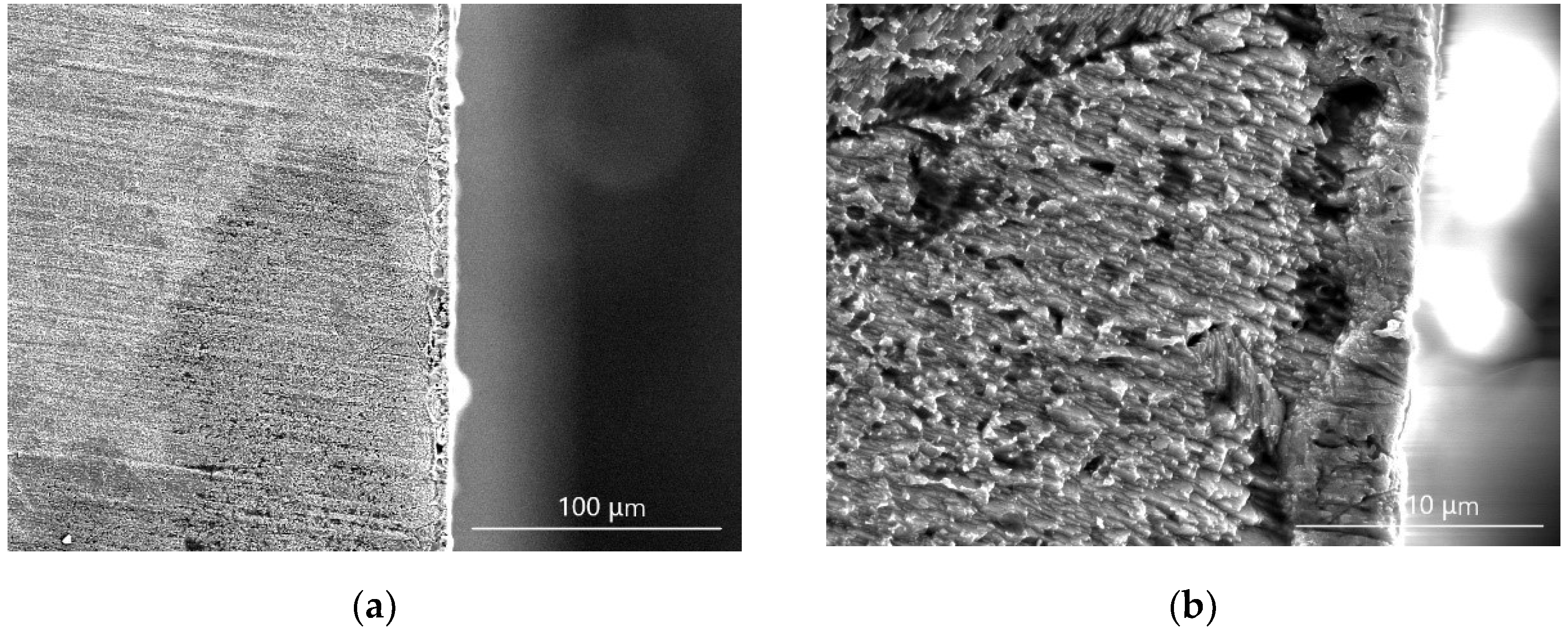
As shown in Figure 1, the content of Ni on the surface of the gradient layer was 27.73%. The surface content of the sample was plated with Ni compared with the surface of pure copper. Figure 2 shows the SEM image of the sample section morphology. As indicated in Figure 2, the Cu–Ni gradient layer is was uniform and had a thickness of about 6 μm. In addition, there was better metallurgical bonding between the plating layer and the substrate. This is because Cu and Ni can form a solid solution, and a gradient layer with a certain thickness can be formed at the interface. This is because, during the process of Ni electrodeposition, the nickel ions in the molten salt migrated to the surface of the cathode copper sheet under the action of an electric field, were reduced to nickel by the electrons, and adhered to the surface of the copper sheet. The nickel then proceeded from the surface to the inside of the copper sheet. Finally, a diffusion layer with a certain nickel content is formed. The process of this diffusion layer is as follows: the nickel ions diffuse from the molten salt to the interface of the copper sheet, then diffuse between the electrical double layers of the interface of electrons participating in the reaction, and then diffuse to the interface into the solid interior.

Figure 1.
Images (left) and spectra (right) of sample surface morphology: (a) image of Cu, (b) spectra of Cu, (c) image of Cu–Ni, (d) spectra of Cu–Ni.
Figure 2.
SEM image of sample section morphology (a) low magnification (b) high magnification.
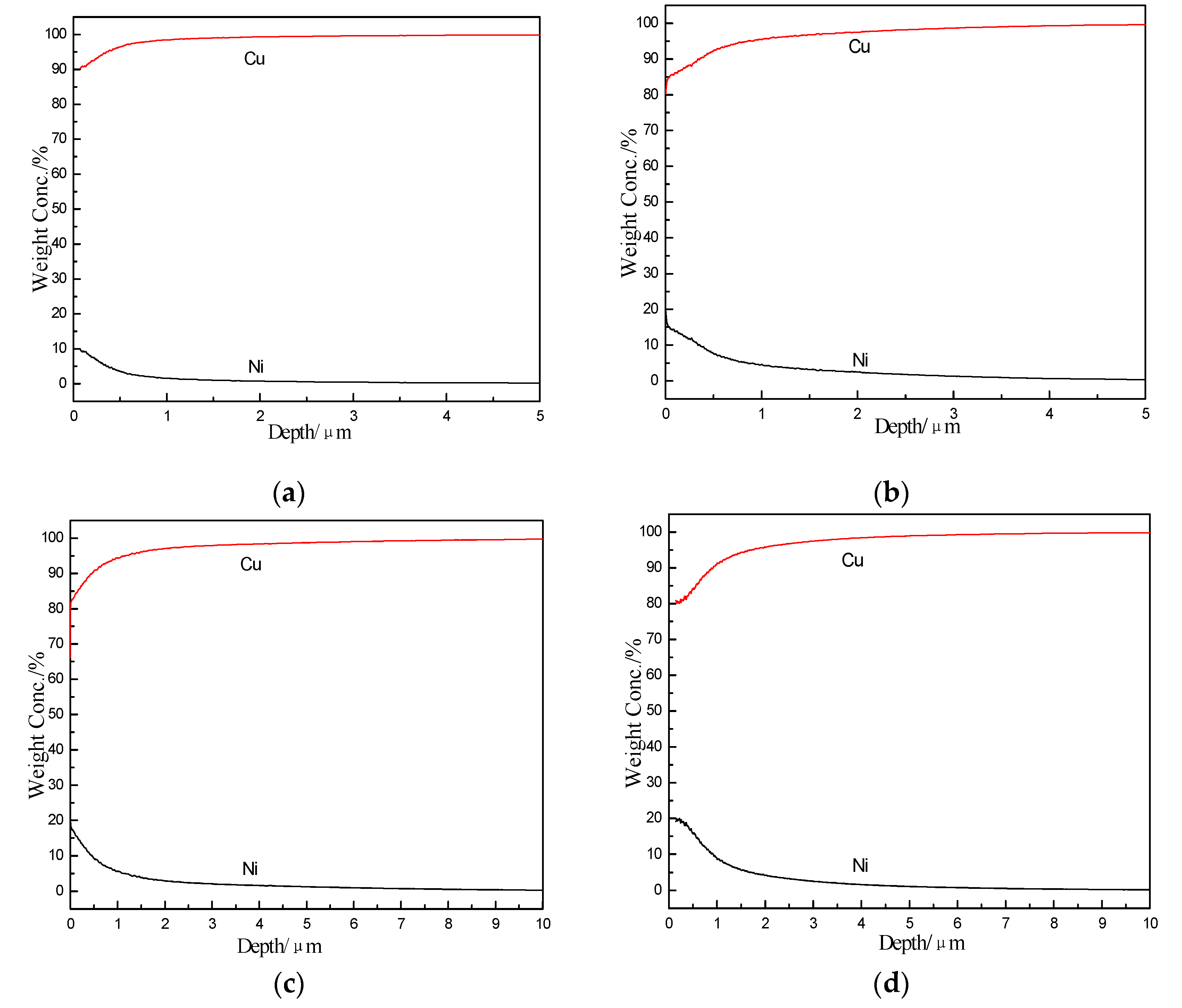
Figure 3 shows the content distribution of Cu, Ni. When the time was at 10 min, the thickness is less than 2 µm. When the time is at 50 min, the thickness was close to 9 µm. As the time increased, the Ni content on the deposition layer presented a growth trend. However, from 30 min to 50 min, the Ni content stayed still. The reason for this phenomenon is that Ni continuously gains electrons to be deposited on the surface of the copper sheet as time goes on in the electrodeposition process. Since the two elements Cu and Ni are completely miscible, the deposited Ni and Cu are solid-state interdiffusion. On the side close to the Cu substrate, the Ni content gradually decreased and had a gradient distribution. The nickel ions on the surface of the copper sheet were gradually consumed as the deposition progresses. The nickel ions in the molten salt needed to be supplemented by diffusion and mass transfer to the cathode copper surface. When the diffusion and mass transfer speed in the molten salt was lower than the electron speed obtained by electrodeposition, the deposition rate was affected due to the diffusion control rate. At the same time, when the inter-diffusion rate of Ni and Cu was much greater than the electrodeposition rate of Ni, Ni continued to diffuse into the Cu substrate, so no pure Ni layer was formed on the surface of the Cu substrate. Solid-state diffusion relies on thermal activation of the atom. Increasing the diffusion rate could not increase the thickness of the graded layer. The probability of atom migration increases with the increase in the transition temperature, and the distance of atom migration increases with the increase in the transition time.
Figure 3.
The content distributing of Cu, Ni at different times: (a) 10 min (b) 20 min (c) 30 min (d) 50 min.
Cu and Ni contact each other to form a Cu/Ni interface, and diffusion occurs at the phase interface during heating. The diffusion behavior of Cu and Ni atoms is different under the same temperature. As the melting point and binding energy of Cu are lower than those of Ni, the temperature during electrodeposition at 700 °C reached 0.65 times the melting point of Cu, so Cu atoms were first thermally activated and began to diffuse; while 700 °C only has the melting point 0.48 times higher than that of Ni, most of the Ni atoms cannot be thermally activated and diffused, and only a very small number of Ni atoms at the lattice distortion defect are thermally activated and diffused. Since the Cu–Ni alloy is a replacement solid solution, the diffusion mechanism is a vacancy diffusion mechanism [22]. At this time, a large number of Cu atoms cross the Cu/Ni interface and migrate to the side of Ni through the vacancy diffusion mechanism, while only a very small number of Ni atoms diffuse and migrate to the side of the Cu.
3.2. The Feature of Ni-W Gradient Layer
The experimental results of depositing W on Ni cathode were analyzed to determine the feasibility of Ni as a connecting metal.
3.2.1. The Analysis of the Constituents
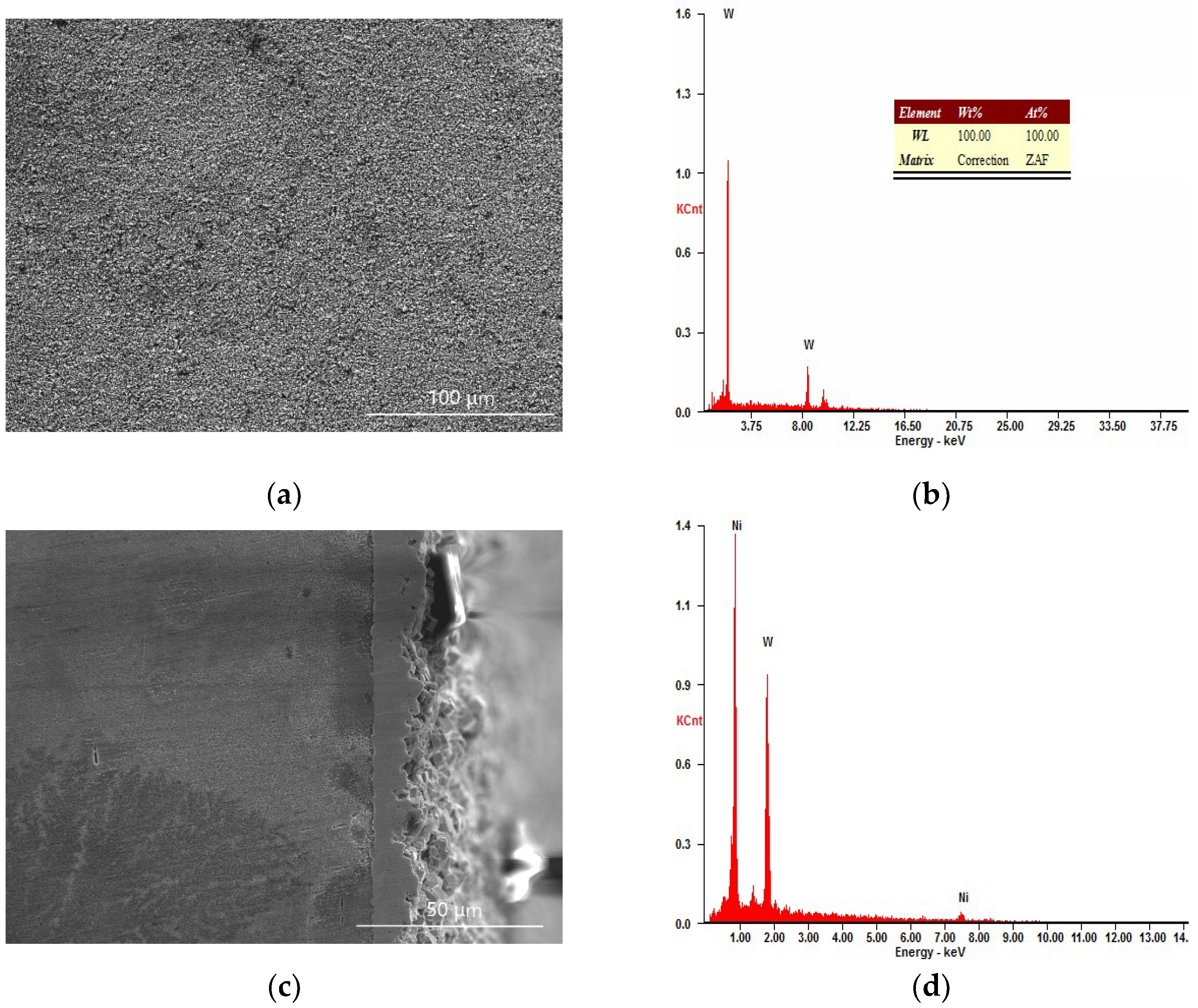
Figure 4 shows the SEM images and EDS spectra of sample surface morphology and section morphology. As indicated in Figure 4, the surface of Ni–W gradient layers is pure W, while both Ni and W are distributed on the cross-section.
Figure 4.
SEM images (left) and EDS spectra (right) of sample: (a) surface SEM images, (b) surface EDS spectra, (c) section SEM images, (d) section EDS spectra.
3.2.2. The Analysis of Sample Cross-section
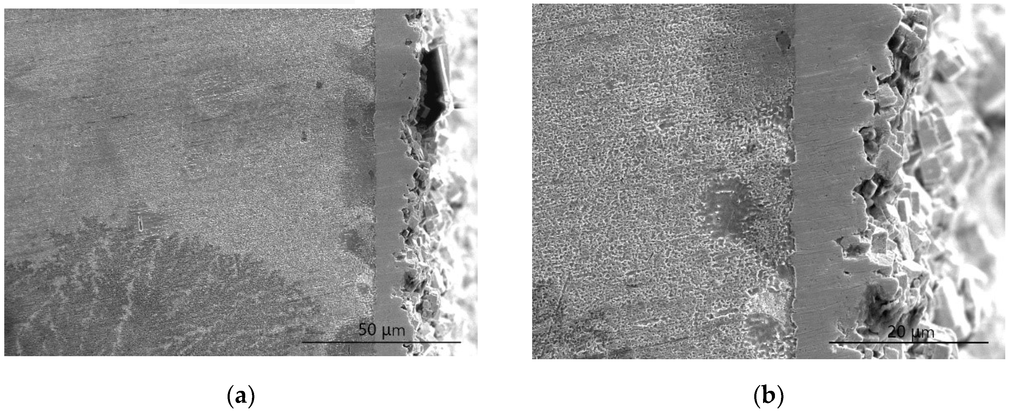
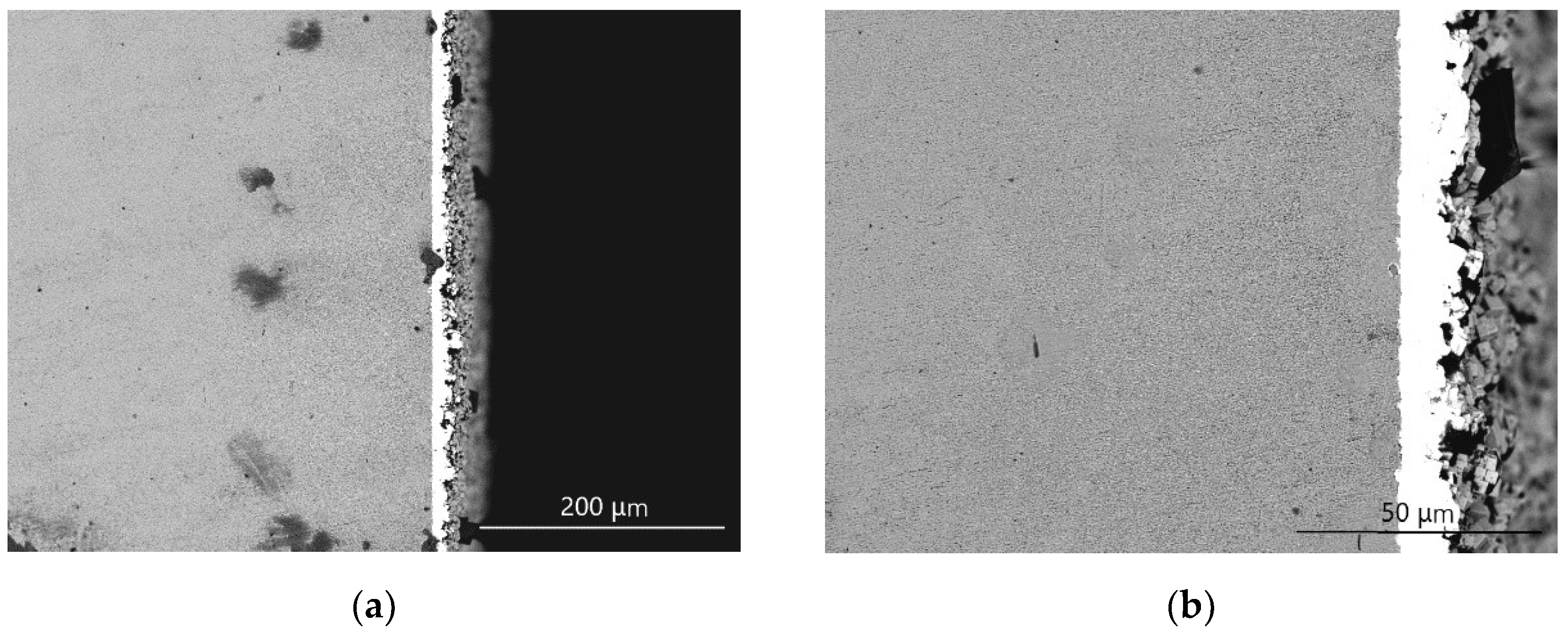
Figure 5 shows an electron microscope photo of the sample cross-section at low and high magnification. It can be seen that the thickness of the coating is uniform at about 10 μm, and the coating is tightly bonded to the substrate. Figure 6 shows the backscattered electron image of sample section morphology. As the principle of Back-Scattered Electron Imaging (BSE) indicates, the coefficient of material of atoms is smaller if the image is darker, whereas the atomic coefficient is larger with a brighter image. Combining this information with that of Figure 5, because there are Ni and W on the cross-section and different back-scattered contrast atoms shows different lightness, the section morphology can be divided into two colors: gray and white. Since the atomic coefficient of W is larger than that of Ni, the white morphology is W, and the gray is Ni. It can also be seen from the figure that the substrate is mainly Ni, and the plating layer obtained by electrodeposition is mainly W. The deposition layer is not only uniform but also well combined with the substrate.
Figure 5.
SEM image of sample section morphology: (a) low magnification (b) high magnification.
Figure 6.
The backscattered electron image of sample section morphology: (a) low magnification (b) high magnification.
From the above analysis, it can be inferred that the Ni–W gradient layer can be obtained in the NaCl–KCl–NaF–WO3 molten salt system. Ni is feasible as a connecting metal of Cu and W.
3.3. The Characteristics of Cu–Ni–W Gradient Layer
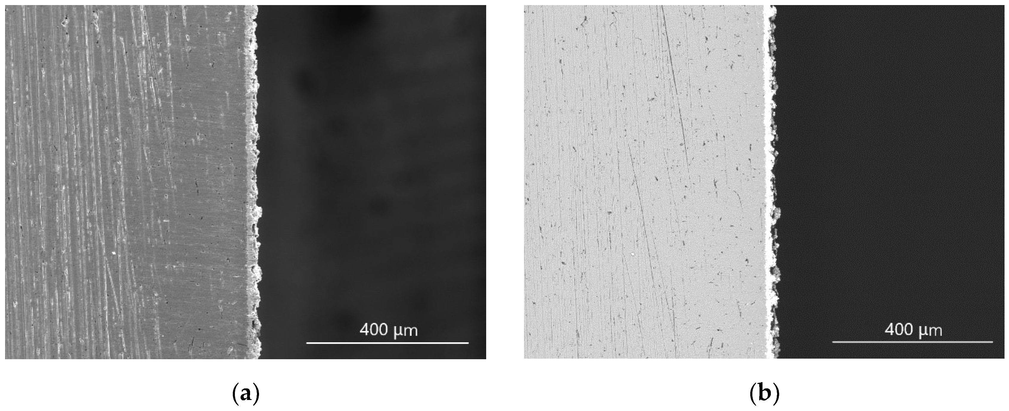
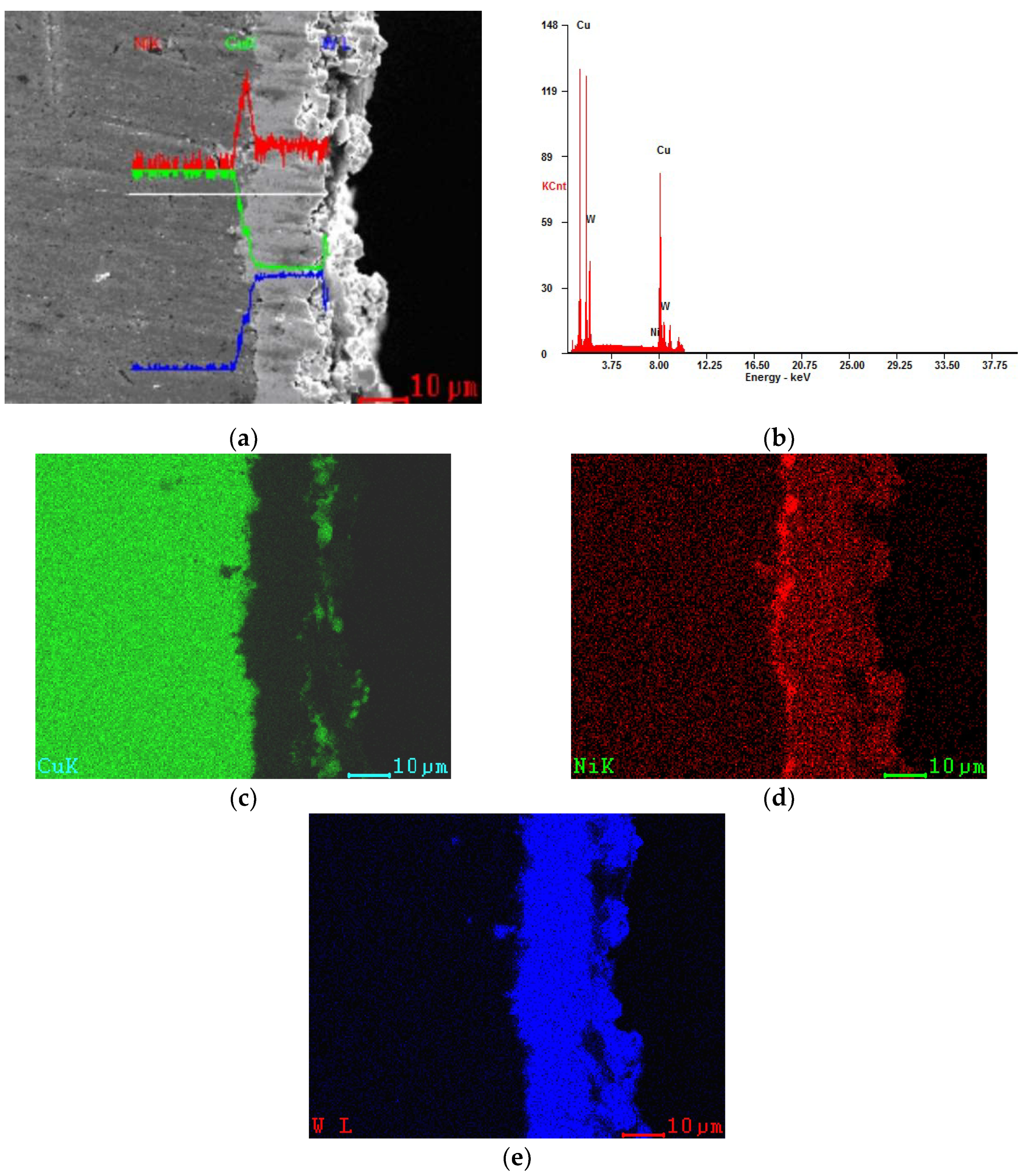
As shown in Figure 7a, the cohesion between the electrodeposition layer and the substrate is close and complete, and there are no cracks and holes. There is also a relatively close cohesion between the electrodeposited layers. Figure 7b shows a backscattered electron image of sample section morphology. Because the atomic coefficient of W is larger than that of Cu and Ni, the white morphology is W. Figure 8 is the EDS surface scanning of the element distribution of Cu, Ni, and W of the sample cross-section. The elements contained in the cross-section of the sample are Cu, Ni, W, and the order of the distribution from the substrate to the outer surface is Cu→Cu + Ni + W→W, where Cu, Ni, and W present a gradient distribution.
Figure 7.
SEM image and backscattered electron image of sample section morphology: (a) SEM (b) backscattered electron image.
Figure 8.
The Cu, Ni, and W element distribution map of sample section EDS surface scanning: (a) SEM, (b) EDS, (c) Cu, (d) Ni, (e) W.
3.4. The Role of Ni to Cu–W Gradient Layer’s Formation
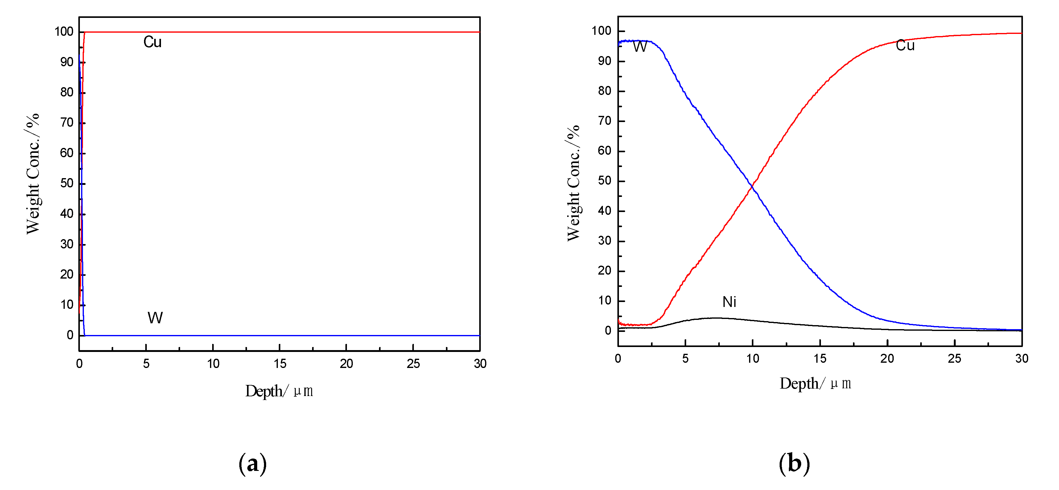
As the bridge between W and Cu, it is easy for Ni to form a solid solution with Cu, and it is easy to form a solid solution of inter-metallic compound with W, which makes W and Cu achieve good properties. This solves the miscibility problem of W and Cu and increases the thickness of the Cu–W gradient layer. Figure 9 shows the content distribution of Cu and W: (a) Cu–W, and (b) Cu–Ni–W. On electrodepositing W, the preparation condition of Cu–Ni–W is the same as that of Cu–W: directional pulse, temperature 700 °C, current density 50 mA·cm−2, and electrodeposition time 10 min. Figure 9 indicates that the thickness of Cu–W gradient layer is 0.5 µm, which can be ignored. The thickness of Cu–Ni–W gradient layer is 12 µm.
Figure 9.
The content distributing of Cu and W: (a) Cu–W and (b) Cu–Ni–W.
At the condition of current density of 50 mA·cm−2, electrodeposition time 10 min, the thickness of Cu–Ni–W gradient layer prepared at the temperature of 700–800 °C is shown in Table 1. Because there is little Ni in the layer, the study only considers the inter-diffusion between Cu and W.
Table 1.
Relationship of the temperature and gradient layer thickness.
Diffusion coefficient and temperature can be expressed as the Arrhenius equation:
where D0 is diffusion coefficient (m2·s−1), Q is diffusion activation energy (J·mol−1), R is gas constant (J·mol−1·K−1), and T is the absolute temperature (K). With the Arrhenius equation and the relationship of permeability thickness and diffusion coefficient, the following equation can be derived [23]:
where δ is the average permeability thickness (m), t is the holding time (s). By taking the logarithm in both sides of the equation, the following equation can be derived:
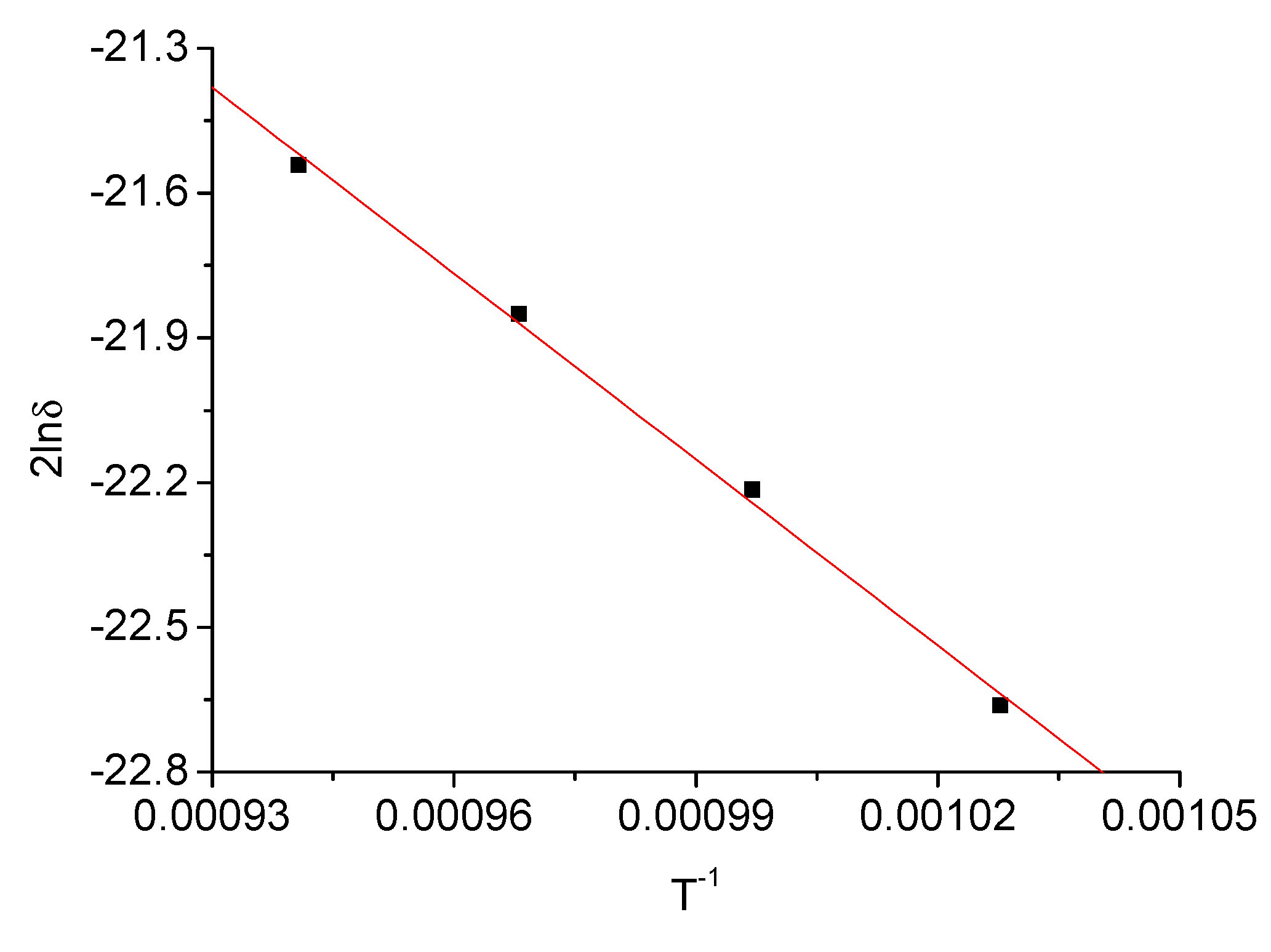
According to the data in Table 1, a scatter diagram was made, which is shown in Figure 10. Fitting a straight line, we get D0 = 1.34 × 10⁻⁷ m2·s−1, Q = 106,880.51 J·mol−1. Substituting D0 and Q into formula (1), the mutual diffusion coefficient at 700 °C is calculated as D = 2.45 × 10⁻¹³ m2·s−1. It can be seen that due to the addition of the Ni element, the inter-diffusion ability of Cu–W becomes larger, the thickness of the gradient layer of Cu–W is enlarged, and the inter-diffusion of Cu and W forms a metallurgical bond, thereby achieving the purpose of alleviating internal stress and forming a good combination of Cu–W functionally graded materials.
Figure 10.
Relationship between 2lnδ and T−1.
4. Conclusions
(1) The condition for obtaining a dense and smooth Cu–Ni gradient layer in a molten salt system with a molar ratio of NaCl:KCl:NaF:NiO = 0.36:0.36:0.25:0.02 is as follows: two-way pulse power supply (pulse cycle: T = 1000 ms, the forward and reverse current ratio: if/ir = 6:1; the forward and reverse time ratio: tf/tr = 3:1), current density of 70 mA·cm−2, electrodeposition temperature of 700 °C, and electrodeposition time of 30 min.
(2) When the molar ratio of the molten salt composition is NaCl:KCl:NaF:WO3 = 0.3385:0.3385:0.25:0.073, the condition for obtaining a dense and smooth Cu–Ni–W gradient layer was as follows: the current density was 50 mA·cm−2, the electrodeposition temperature was 700 °C, bidirectional pulse electrodeposition was used, and the electrodeposition time was 20 min.
(3) The addition of Ni element promotes the inter-diffusion between Cu and W. The inter-diffusion coefficient at 700 °C is calculated to be D = 2.45 × 10⁻¹³ m2·s−1. The addition of Ni greatly increased the mutual diffusion coefficient D of Cu–W. The thickness of the gradient layer of Cu–W can reach 21 μm. Cu and W form a metallurgical bond, thereby achieving the purpose of alleviating internal stress and forming a well-bonded Cu–W functionally graded material.
Author Contributions
Conceptualization, H.L.; data curation, J.L.; writing—original draft preparation, H.Y.; writing—review and editing, Y.L.; visualization, L.W. All authors have read and agreed to the published version of the manuscript.
Funding
This research was funded by the National Natural Science Foundation of China, grant number 51774143.
Data Availability Statement
Not applicable.
Acknowledgments
This work was supported by the National Natural Science Foundation of China (No. 51774143).
Conflicts of Interest
The authors declare no conflict of interest.
References
- Ge, C.C.; Zhou, Z.; Ling, Y.H. New progress of metal-based functionally graded plasma-facing materials in China. Mater. Sci. Forum 2003, 423, 11–16. [Google Scholar] [CrossRef]
- Han, J.C.; Xu, L.; Wang, B.L.; Zhang, X.H. Progress and prospects of functional gradient materials. J. Solid Rocket Technol. 2004, 27, 207–215. [Google Scholar]
- Ling, Y.; Bai, X.; Zhou, Z.; Li, J.; Ge, C. Thermal shock behavior of W/Cu functionally gradient material. Rare Met. Mater. Eng. 2004, 33, 819–822. [Google Scholar]
- You, J.H.; Bolt, H. Analytical method for thermal stress analysis of plasma facing materials. J. Nucl. Mater. 2001, 299, 9–19. [Google Scholar] [CrossRef]
- Chapa, J.; Reimanis, I. Modeling of thermal stresses of a graded Cu/W joint. J. Nucl. Mater. 2002, 303, 131–136. [Google Scholar] [CrossRef]
- Senderoff, S.; Mellors, G. Coherent coatings of refractory metal. Science 1966, 153, 1475–1481. [Google Scholar] [CrossRef] [PubMed]
- Masuda, M.; Takenishi, H.; Katagiri, A. Electrodeposition of tungsten and related voltammetric study in a basic ZnCl2-NaCl (40–60 mol %) melt. J. Electrochem. Soc. 2001, 148, C59. [Google Scholar] [CrossRef]
- Pavlovskii, V.A. Tungsten galvanic coatings deposited from salt melts. Prot. Met. 2006, 42, 170–173. [Google Scholar] [CrossRef]
- Pavlovskii, V.A. Density and electrical conductivity of NaF–NaCl–WO3 melts. Inorg. Mater. 2003, 39, 1208–1211. [Google Scholar] [CrossRef]
- Koyama, K.; Morishita, M.; Umezu, T. Design of molten salt bath on the basis of acid-base cooperative reaction mechanism. Smooth electrodeposition of tungsten from KF-B2O3-WO3 molten salt. Electrochemistry 1999, 67, 677–683. [Google Scholar] [CrossRef]
- Nitta, K.; Nohira, T.; Hagiwara, R.; Majima, M.; Inazawa, S. Characteristics of a tungsten film electrodeposited in a KF–B2O3–WO3 melt and preparation of W–Cu–W three-layered films for heat sink application. J. Appl. Electrochem. 2010, 40, 1443–1448. [Google Scholar] [CrossRef]
- Boire-Lavigne, S.; Moreau, C.; Saint-Jacques, R. Relationship between the microstructure and thermal diffusivity of plasma-sprayed tungsten coatings. J. Therm. Spray Technol. 1995, 4, 261–267. [Google Scholar] [CrossRef]
- Dhote, A.; Ogale, S. Deposition of tungsten films by pulsed excimer laser ablation technique. Appl. Phys. Lett. 1994, 64, 2809–2811. [Google Scholar] [CrossRef]
- Varacalle, D.J., Jr.; Lundberg, L.; Jacox, M.; Hartenstine, J.; Ii, W.; Herman, H.; Bancke, G. Fabrication of tungsten coatings and monoliths using the vacuum plasma spray process. Surf. Coat. Technol. 1993, 61, 79–85. [Google Scholar]
- Philipps, V. Tungsten as material for plasma-facing components in fusion devices. J. Nucl. Mater. 2011, 415, 2–9. [Google Scholar] [CrossRef]
- Maier, H.; Kötterl, S.; Krieger, K.; Neu, R.; Balden, M. Performance of tungsten coatings as plasma facing components used in ASDEX Upgrade. J. Nucl. Mater. 1998, 258, 921–926. [Google Scholar] [CrossRef]
- Fan, J.L.; Yan, D.J.; Huang, B.Y. The current research status of W–Cu composite material at home and abroad. Powder Metal. Ind. 2003, 13, 9–14. [Google Scholar]
- Riccardi, B.; Montanari, R.; Casadei, M.; Costanza, G.; Chioni, G. Optimisation and characterisation of tungsten thick coatings on copper based alloy substrates. J. Nucl. Mater. 2006, 352, 29–35. [Google Scholar] [CrossRef]
- Liu, X.; Yang, L.; Tamura, S.; Tokunaga, K.; Yoshida, N.; Noda, N.; Xu, Z. Thermal response of plasma sprayed tungsten coating to high heat flux. Fusion Eng. Des. 2004, 70, 341–349. [Google Scholar] [CrossRef]
- Liu, Q.; Zhang, Y.; Liu, Y.; Xu, L.; Jiang, F. Research development of electrodeposited tungsten and tungsten alloys coating. Int. Mater. Rev. 2012, 26, 142–146. [Google Scholar]
- Wang, X.Y.; Yang, H.L.; Feng, C.; Wang, Y.L.; Li, Y.G. Relationship between primary crystallization temperature of NaCl-KCl-NaF molten salt system and composition. Nonferr. Met. 2015, 5, 62–65. [Google Scholar]
- Zhao, P.; Xie, F.Z.; Sun, W.S. Materials Science; Harbin Institute of Technology Press: Harbin, China, 1999; pp. 163–164. [Google Scholar]
- Cui, M.; Zhao, P. The Effect of cold plastic deformation on nitrogen in the deffusion activation energy of 38CrMoAlA steel. J. Met. Heat Treat. 1994, 15, 48–54. [Google Scholar]
Publisher’s Note: MDPI stays neutral with regard to jurisdictional claims in published maps and institutional affiliations. |
© 2021 by the authors. Licensee MDPI, Basel, Switzerland. This article is an open access article distributed under the terms and conditions of the Creative Commons Attribution (CC BY) license (https://creativecommons.org/licenses/by/4.0/).