Article

Both Symmetric and Asymmetric Electro-Optic Dynamic Behavior with SSD (Smectic Single Domain) Liquid Crystals

by
Akihiro Mochizuki
i-CORE Technology, LLC, 400 Orchard Dr., Louisville, CO 80027, USA
Crystals 2021, 11(4), 337; https://doi.org/10.3390/cryst11040337
Submission received: 5 March 2021 / Revised: 20 March 2021 / Accepted: 22 March 2021 / Published: 26 March 2021

Abstract

:
SSD-liquid crystal panels’ retardation switching dynamic behaviors have been investigated from their in-plane and out-of-plane retardation switching behaviors. In-plane-only and a mixture between in-plane and out-of-plane retardation switching behaviors are highly related to the initial smectic liquid crystal molecular stacking configurations. With uniformly stacked configuration, a completely symmetric retardation switching, as well as light throughput behavior, was obtained. With a slight twisted stacking configuration, the retardation switching behavior is dependent on the applied electric field strength, which may change the initial molecular stacking configuration, resulting in either symmetric or asymmetric retardation switching. When the molecular stacking has twisted heavily, the obtained retardation switching showed asymmetric behavior regardless of the applied electric field strength.

1. Introduction

A smectic single domain (SSD) liquid crystal mode shows some unique electro-optic dynamic behaviors, including in-plane-only retardation switching [1]. Some empirical research works on a Smectic Single Domain-Liquid Crystal (SSD-LC) drive mode have revealed both clear phenomena and unclear phenomena in terms of racial interpretation. A clear phenomenon is the relationship between retardation switching nature and the initial smectic liquid crystal molecular stacking configurations [2]. An unclear phenomenon is the mixing behavior between in-plane and out-of-plane retardation switching. In-plane-only retardation switching is expected to be applied to some practical uses, including phase-only switching devices, beam steering devices, and so on. Many of these newer uses of liquid crystals require a much faster optical response than those for current display devices. An SSD-LC panel enables a sub-millisecond optical response time with a decent driving voltage [3]. Studies limited to the faster optical response performance of several liquid crystal driving modes have been carried out, including surface-stabilized ferroelectric liquid crystals (SSFLCs) [4,5], DeVries type of smectic A phase liquid crystals [6,7,8,9,10], anti-ferroelectric liquid crystals (AFLCs) [11,12,13], distorted helix ferroelectric liquid crystals (DH-FLCs) [14,15], flexo-electric liquid crystals [16,17,18,19], some different types of blue phase liquid crystals [20,21], and so on. Most of these faster optical response liquid crystal drive modes, however, show both in-plane and out-of-plane retardation switching at their switching process. A flexo-electric liquid crystal theoretically enables in-plane-only retardation switching. However, such a flexo-electric response liquid crystal requires an applied electric field parallel to the liquid crystal panel substrates. Due to the fringe field effect, it is not easy to obtain a complete parallel applied electric field to a liquid crystal layer. Therefore, from a practical point of view, it is important to show in-plane-only retardation switching with a electric field vertically applied to a liquid crystal layer, which is similar to current liquid crystal display device configurations. An SSD-LC drive mode enables such vertically applied drive voltages to obtain in-plane-only retardation switching [22]. In the course of detailed research into an SSD-LC drive mode, it was found that in-plane-only retardation switching is strongly related to the smectic liquid crystal molecular packing configuration. In some cases, some mixture between in-plane and out-of-plane retardation switching was observed; in other cases, strong out-of-plane retardation switching was observed. Moreover, it was also found that the applied electric field polarity response SSD-LC drive mode sometimes shows a symmetric optical response to the applied electric field polarity, but it also sometimes shows an asymmetric optical response. Such symmetric and asymmetric optical responses are reasonably assumed to be attributed to the initial smectic liquid crystal molecular packing configuration. This report focuses on a symmetric and an asymmetric optical response behavior in terms of retardation switching behavior. To clarify the relationship between retardation switching dynamics and an initial liquid crystal molecular stacking configuration, some optical measurement approaches have been investigated to distinguish in-plane and out-of-plane retardation switching.

2. About an SSD-LC Drive Mode

An ideal configuration of the SSD-LC drive mode is illustrated in Figure 1. A tilted smectic liquid crystal molecule, such as SmC, SmH, and SmI sub-phased liquid crystal molecule as a bulk state, is stacked uniformly in parallel to the substrates, as shown in Figure 1. Due to strong azimuthal anchoring, tilted smectic liquid crystal molecules align parallel to the surface initial alignment direction, such as the mechanical buffing direction. Under the crossed Nicol optical setup, as a normally black configuration, the SSD-LC panel shows light throughput depending on the applied electric field strength. The SSD-LC molecules swing in the same, originally aligned plane, and the swing angle is dependent on the applied electric field strength. Whether the swing direction is clockwise or counter-clockwise is dependent on the applied electric field direction, such as upward or downward, at the SSD-LC panel.
The SSD-LC molecules swing, and switching in the same plane as originally aligned enables in-plane-only retardation switching by the vertically applied electric field, as shown in Figure 1. The current obtained maximum swing angle at an SSD-LC panel is ca. 75 degrees both clockwise and counterclockwise, respectively.

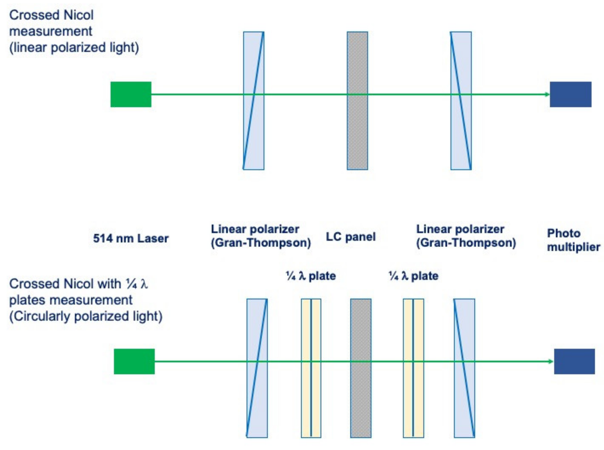
3. Empirical Approach to Distinguish In-Plane and Out-of-Plane Retardation Switching

When an almost uniformly stacked smectic liquid crystal molecule is obtained, the SSD-LC panel shows in-plane-only retardation switching. Although intrinsic in-plane/out-of-plane retardation switching behavior is measurable by using a pair of photo-elastic modules [22], there is a simpler optical measurement, made by observing a comparison between a linearly polarized incident beam and a circularly polarized incident beam, which enables separation between in-plane-only, or a mixture between in-plane and out-of-plane, retardation switching. This measurement set-up is shown in Figure 2.
The used SSD-LC mixtures are phenyl-pyrimidine-based smectic liquid crystal mixtures, with their bulk state tilted to the smectic layer [3,22]. For an expected uniformly stacked SSD-LC panel, a low pre-tilt alignment layer with mechanical buffing as a parallel configuration was applied. For an expected, slightly twisted stacked SSD-LC panel, a medium pre-tilt alignment layer with mechanical buffing as an anti-parallel configuration was applied. For an expected heavily twisted stacked SSD-LC panel, a high pre-tilt alignment layer with mechanical buffing as a parallel configuration was applied. All panels maintained their panel gaps using 2.5 μm silica spacer balls.
In Figure 2, the upper set-up is typical for an amplitude modulation measurement using a linearly polarized incident beam. The lower set-up uses a circularly polarized incident beam. When a sample liquid crystal panel only switches the phase without any change in the amplitude of an incident beam, the liquid crystal panel gives an in-plane-only retardation switching. When a sample liquid crystal panel shows any amplitude change, at both measurement set-ups, the sample panel gives a mixture between in-plane and out-of-plane retardation switching. For confirmation purposes, before an SSD-LC panel was measured, both an Electrically Controlled Birefringence (ECB) mode liquid crystal panel and a Twisted Nematic (TN) mode liquid crystal panel were compared for their in-plane and out-of-plane retardation switching behavior. Figure 3 and Figure 4 represent an ECB and a TN panel case, respectively.
As shown in the Figure 3 upper viewgraph, an ECB-LC panel shows immediate light intensity reduction by an applied pulse voltage to the linearly polarized incident beam. The lower viewgraph in Figure 3 for a circularly polarized incident beam shows similar light-throughput behavior to the upper viewgraph. However, during pulse voltage application, a linearly polarized case shows some increase in light throughput, while a circularly polarized case shows it as almost flat. This dynamic light-throughput behavior suggests some in-plane and out-of-plane retardation switching behavior. In the ECB-LC panel, the initial planar aligned liquid crystal molecules change their directors to perpendicular to the substrates. This director change is very quick, as seen in the lower viewgraph of Figure 3. Once turned, some liquid crystal directors perpendicular to the substrates seem to rearrange each other, keeping their directors mostly perpendicular to the substrates. Such behavior leads to total retardation change during the pulse voltage application. Even total retardation shows some increase in its light intensity. Light intensity to a circularly polarized incident beam shows almost no change. The reasonable interpretation of these light intensity changes, shown in Figure 3, is that once turned, liquid crystal molecular directors perpendicular to the substrates remain perpendicular; however, they rearrange the directors in the plane perpendicular to the substrates. Even the director movement would be small; such a director rearrangement move gives some small retardation change, as shown in the upper viewgraph in Figure 3. After removing the applied pulse voltage, the opposite director movement occurs. Right after removing the applied voltage, most of the liquid crystal molecular directors turn parallel to the substrates; however, there is not a singular path from perpendicular to parallel, but many. After the director turns parallel to the substrates, each director starts to rearrange to the initial alignment. This process is within the same plane, or in-plane retardation only. The different light intensity dynamics after the removal of the applied pulse voltage between linearly and circularly polarized incident beams clearly suggests such dynamic behavior.
A TN-LC panel case also gives the liquid crystal molecular director dynamic behavior, as shown in Figure 4. As shown in Figure 4, at a TN-LC panel case, even the total retardation switching shows a relatively fast recovery after the applied pulse voltage is removed in the upper viewgraph of Figure 4; out-of-plane retardation switching takes a relatively longer time to come back to the initial alignment.
As shown both in Figure 3 and Figure 4, it is clear that Figure 2 measurement setups provide some detailed molecular director switching dynamic behavior.

4. Results and Discussion

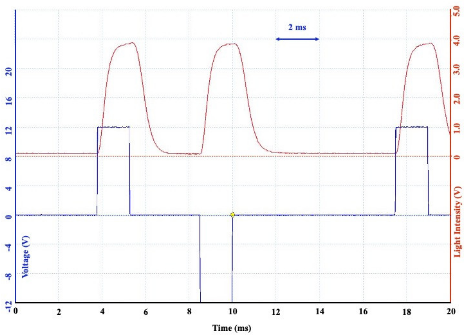
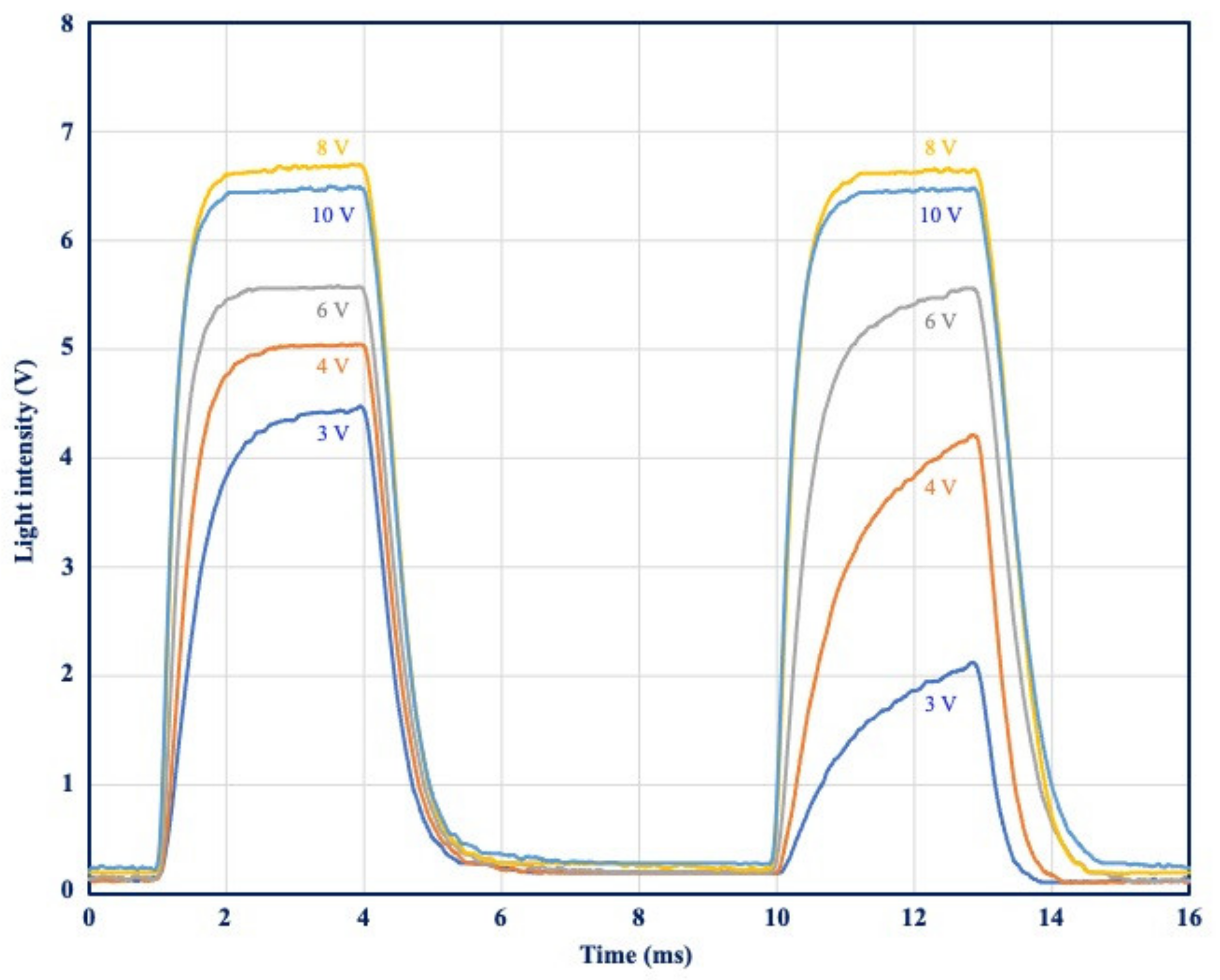
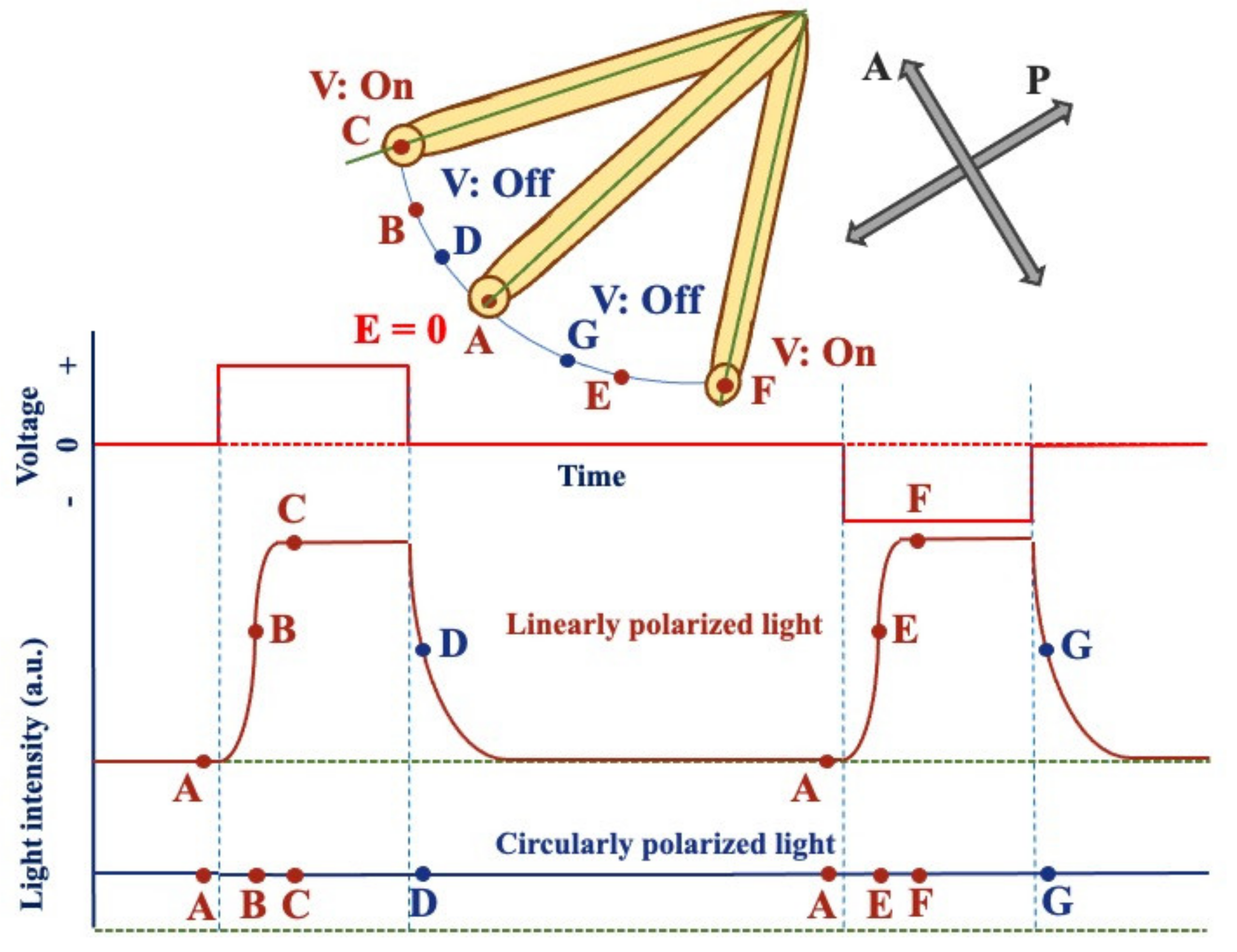
4.1. Some Retardation Switching Variation in an SSD-LC Panel

With a uniform enough molecular stacking, Figure 5 and Figure 6 show almost in-plane-only retardation switching in an SSD-LC drive mode panel, respectively.
Scheme 1 shows this sample panel’s texture photo under crossed Nicols conditions. Due to the single domain smectic liquid crystal nature of an SSD-LC panel, no particular textures are observed, and during its electro-optic switching under crossed Nicols, the light throughput simply changes its intensity, without showing any texture changes. Regardless of smectic layer structure, as long as each SSD-LC molecule has an initial uniformly stacked configuration, most of the uniformly stacked SSD-LC molecules have commensurate movement, resulting in a single domain texture without showing any observable level of textures.
The SSD-LC panel gives a fast optical response for a linearly polarized incident beam, such as around 200 μs on and off response times, respectively, as shown in Figure 5. Applying the same drive voltage, a circularly polarized incident beam does not show any significant amplitude change, as shown in Figure 6.
The comparison between Figure 5 and Figure 6 suggests that the SSD-LC panel provides in-plane-only retardation switching. One of the possible supporting results explaining why this SSD-LC panel has uniformly stacking liquid crystal molecules in the panel is observed in Figure 7. Figure 7 shows the applied pulse voltage dependence on light throughput for linearly polarized incident beam. The applied pulse voltage duration is 3 ms, with a 5 ms zero-volt interval.
This SSD-LC panel shows an almost symmetric optical throughput both for a positive pulse and a negative pulse. The first peaks in Figure 7 correspond to positive a 3 ms duration pulse, and the second peaks correspond to a negative pulse. As shown in Figure 7, the SSD-LC panel has an almost symmetric optical response to a bipolar pulse voltage drive, as well as almost constant optical response times, regardless of the variation in pulse voltage. This applied voltage-insensitive response time is also one of the unique features of an SSD-LC panel [1,2].
An almost symmetric optical response dynamic behavior indicates uniform stacked SSD-LC molecules and their consecutive in-plane-only retardation switching in the same plane with the original liquid crystal molecular alignment.
On the other hand, when some partial-twisting molecular stacking is included in the initial molecular stacking, the light-throughput dynamic behavior is different from those shown in Figure 5, Figure 6 and Figure 7. Figure 8 and Figure 9 show the case of a non-uniformly stacked SSD-LC panel.
The expectedly slightly twisted configured SSD-LC panel’s texture photo is shown in Scheme 2. Even a comparison between Figure 8 and Figure 9 suggests some significant retardation switching behavior difference, with the uniformly stacked SSD-LC panel shown in Figure 5 and Figure 6. The two panels’ textures are not so different, as shown in Scheme 2. It is assumed that, unlike spontaneous polarization-based smectic liquid crystal panel cases such as SSFLCDs, DeVries types, non-spontaneous polarization SSD-LC panels’ texture under a crossed Nicols condition is much more similar to those for uniaxially aligned nematic liquid crystal panels.
The comparison between Figure 8 and Figure 9 suggests that the non-uniformly stacked SSD-LC panel provides some light throughput change to the circularly polarized incident beam when bipolar pulse voltage is applied. Figure 9 shows some out-of-plane retardation change in conjunction with in-plane retardation change; therefore, in the SSD-LC panel, at least some liquid crystal molecules switch outside the original plane. The Figure 9 case also shows an almost symmetric out-of-plane retardation change to positive and negative pulse voltage. This slightly twisted expected SSD-LC panel shows a different behavior in the applied voltage dependence of light throughput to a linearly polarized incident beam, as shown in Figure 10. Unlike the uniformly stacked case shown in Figure 7, the expected slightly twisted SSD-LC panel shows asymmetric light throughput up to 6 V. However, over 8 V, the response to both positive (the first peaks) and negative (the second peaks) pulse voltages are symmetric in their light throughput dynamic behaviors. From Figure 8, Figure 9 (12 V pulse voltage), and Figure 10, it is assumed that the implemented initial slight-twist stacking structure would be released by a stronger applied electric field strength. Once the initial, slight-twist-stacking of molecules is released, the optical response dynamic behavior becomes symmetric in response to applied bipolar pulse voltages. To carry out further investigations, other molecular stacking situations were investigated. Figure 11 and Figure 12 show some asymmetric out-of-plane retardation switching cases.
This asymmetric out-of-plane retardation switching panel’s texture under crossed Nicols is shown in Scheme 3.
Unlike in Figure 9, Figure 12 shows asymmetric out-of-plane retardation switching. In this expectedly heavily twisted stacked SSD-LC panel, the applied pulse voltage dependence of light for the linearly polarized incident beam is shown in Figure 13.
Similar to the Figure 10 case with the expected slightly-twisted stacking panel, the Figure 13 case shows asymmetric light-throughput dynamic behavior. The similarity between Figure 10 and Figure 13 is asymmetric light throughput and symmetric light throughput at a higher applied voltage, such as over 10 V. The difference is an applied pulse voltage dependence of light throughput at the second peaks (negative pulse voltage). Unlike the Figure 10 case, the light-throughput level does not show any leap, as shown in Figure 10 between 8 V and 10 V. This difference indicates that no applied electric field strength release of the implemented twisting structure at the Figure 13 case, unlike the Figure 10 case. Both Figure 8, Figure 9, and Figure 11, Figure 12 cases were based on non-uniformly stacked liquid crystals configuration. The out-of-plane retardation switching behavior difference shown in Figure 9 and Figure 12 indicates some molecular-stacking structure differences, and its consecutive smectic layer structure difference.

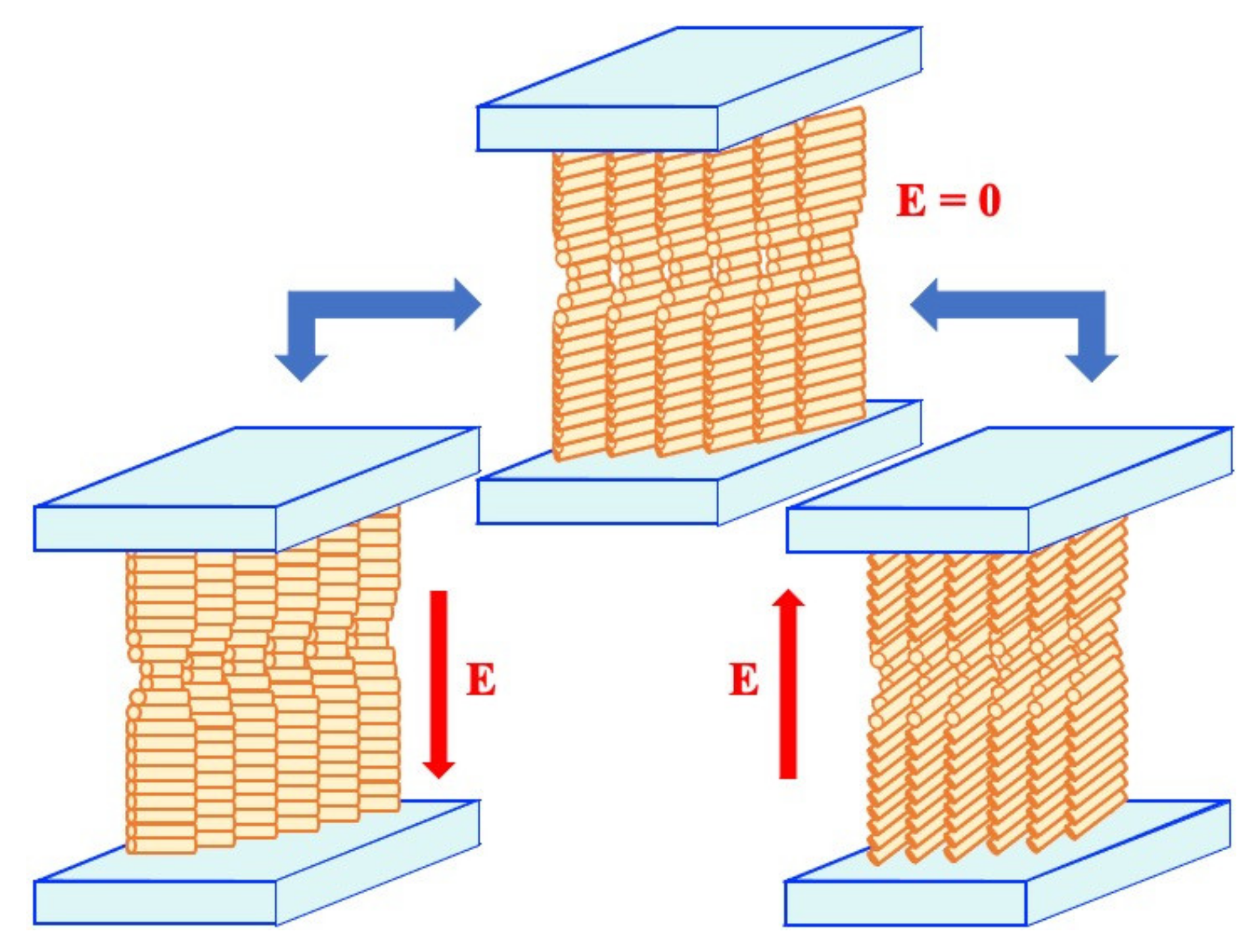
4.2. Molecular Switching Dynamic Models in an SSD-LC Panel

Based on the empirically observed results shown above, the following three different molecular switching dynamic models are conceivable. The first case is for Figure 5 and Figure 7. The second case is for Figure 8 and Figure 9. The third case is for Figure 11 and Figure 12.

4.2.1. Uniformly Stacked SSD-LC Case

Figure 14 illustrates the expected SSD-LC molecular director switching behavior. In the uniformly stacked case, the SSD-LC molecule switches in the single plane (the initial aligned plane). The initial position of the molecule is as the position A shown in Figure 14. When positive pulse voltage is applied to the panel, the SSD-LC molecule swings to position B and then reaches the final position C. All the swing paths from position A, position B and position C are in the same plane. When the applied positive pulse voltage is removed, the SSD-LC molecule swings back to position D and reaches the original position A through the same plane. When negative pulse voltage is applied and removed, the SSD-LC molecule swings in the opposite direction, but in the same plane, as illustrated in Figure 14.
Based on the observed empirical results and considerations given above, it is reasonably assumed that the SSD-LC molecules of the panel have a uniformly stacked configuration, as in the initial state, and during molecular switching by an externally applied vertical electric field, the molecular stacking maintains its uniform stacking configuration, as illustrated in Figure 15. The expected uniform stacking of SSD liquid crystals may be attributed to a low surface pre-tilt, in addition to the so-called parallel mechanical buffing configuration, as at least one of the decisive factors. It would require more factors to provide a uniform molecular stacking at an SSD-LC panel and would require further investigation, specifically into local smectic layer structures.

4.2.2. Slightly Twisted SSD-LC Case

Figure 16 illustrates the expected SSD-LC molecular director switching behavior of the slightly twisted SSD-LC panel. In the slightly twisted stacked case, the SSD-LC molecule lifts slightly, as illustrated in Figure 16, from the initial position A to position B, position C, and then reaches position D. Both positions B and C are out-of-plane from the initial aligned plane. The final position D is located in the same plane as position A. When the applied positive pulse voltage is removed, the SSD-LC molecule swings back from position D to position A through the positions E and F. Although positions B, C and positions E, F are out-of-plane from the initial aligned plane, the swing path from position A to position D, and position D to position A are the same path. When a negative pulse voltage is applied and removed, the SSD-LC molecular swing path is the same as the one with a positive pulse voltage application case, but the opposite direction from the positive pulse application case, as illustrated in Figure 16.
The out-of-plane retardation switching behavior measured in Figure 9 is reasonably interpreted for the double peaks when a pulse voltage is applied and removed, as illustrated in Figure 16. Based on the above consideration, the expected initial molecular stacking configuration and its switching behavior are illustrated in Figure 17. It is still not completely clear why such slight-twisting molecular stacking occurs. A medium surface pre-tilt angle and a so-called anti-parallel mechanical buffing configuration may be one of the factors providing such a slight twisting configuration.

4.2.3. Heavily Twisted SSD-LC Case

Figure 18 illustrates the expected SSD-LC molecular director switching behavior of the heavily twisted SSD-LC panel. In the heavily twisted stacked case, the SSD-LC molecule lifts slightly, as illustrated in Figure 18, from the initial position A to position B, position C, and reaches position D. All the positions, B, C and D, are out-of-plane from the initial aligned plane. Unlike the slightly-twisted case illustrated in Figure 16, in the heavily-twisted case, the lift-up from the initial aligned plane is increasing as the molecular swing proceeds from position A to position D, as illustrated in Figure 18. When negative pulse voltage is applied, however, the molecular swing behavior is different from that of positive pulse voltage case. The molecule stays at the same plane as the initial aligned plane. Therefore, in the heavily twisted case, the molecular swing is asymmetric in terms of in-plane and out-of-plane retardation switching.
Based on the above measurement results and consideration, the expected initial, and during switching states, molecular stacking configuration is illustrated in Figure 19. Unlike the slightly twisted initial molecular stacking case illustrated in Figure 17, the heavily twisted case may not be altered by the applied electric field. Due to the heavily-twisted configuration, the molecular switching has an easy direction and a hard direction. In this case, an easy direction may provide in-plane-only retardation switching, and a hard direction may provide out-of-plane retardation switching. This type of asymmetric electro-optic response in terms of out-of-plane retardation switching has been only observed with a so-called parallel mechanical buffing configuration, using a surface alignment layer having a high surface pre-tilt angle. At this stage of investigation, this is still just an assumption; however, a high surface pre-tilt angle with parallel mechanical buffing may enhance the twisting structure in the SSD-LC panel. Since the SSD-LC molecule has an intrinsically molecular tilt angle to the smectic layer normal as a bulk, even surface anchoring prevents the molecular tilt in the SSD-LC panel, and it is still leaving some intrinsic twisting in the panel. Due to the twisting direction of the bulk liquid crystal molecules, it is reasonably assumed to have an easy and hard twisting direction.

5. Conclusions

SSD-LC molecular switching dynamics have been discussed in terms of initial molecular stacking configuration. Investigation into both in-plane and out-of-plane retardation switching dynamics has revealed a unique relationship between the initial molecular stacking configuration and molecular switching behavior. When the expected smectic liquid crystal molecular stacking is uniform, the liquid crystal molecular switching is in the same plane as where the liquid crystal molecules initially aligned. The molecules swing in the same plane, and the swing direction is a uniquely dependent on the applied electric field direction perpendicular to the liquid crystal layer. Since the molecular switching is always perpendicular to the applied electric field, the obtained retardation switching is always in-plane-only. At the slightly twisted stacking configuration, retardation switching behavior is dependent on the applied electric field strength. When the applied electric field strength is weak enough, due to the twisted structure, the SSD-LC panel provides a mixture of in-plane and out-of-plane retardation switching. When the applied electric field is strong enough to release the slightly twisting configuration, the retardation switching provided is in-plane-only, similar to that of the uniformly stacked configuration panel. With the heavily twisted stacking configuration, an externally applied electric field strength seems inadequate to release the twisting structure, resulting in asymmetric retardation switching. Due to the heavily twisted configuration, there are both easy and hard swing directions from the applied electric field. The easy swing direction almost provides in-plane-only retardation switching, and the hard swing direction provides out-of-plane retardation switching.
Although there are still some unclear phenomena with an SSD-LC driving mode, the current obtained empirical, and some theoretical, assumptions lead to the possible use of in-plane-only, and a mixture of in-plane and out-of-plane, retardation switching. In-plane-only retardation switching would have some benefits to phase-only modulation devices as well as high-efficiency diffraction devices, including non-mechanical beam steering devices. A controllable ratio between in-plane and out-of-plane retardation switching would enable some optical switching devices for three-dimensional optical switching purposes.
Some further investigation into a larger swing angle, such as both 90 degrees clockwise and 90 degrees counter-clockwise, would also be a great attraction for a high-efficiency phase-only switching device.

Funding

This research received no external funding.

Conflicts of Interest

The authors declare no conflict of interest.

References

  1. Mochizuki, A. In-Plane Only Retardation Switching by Certain Type of Smectic Liquid Crystal Panels. In Proceedings of the Emerging Liquid Crystal Technologies XIII, San Francisco, CA, USA, 27 January–1 February 2018; Society of Photo-Optical Instrumentation Engineers (SPIE): Bellingham, WA, USA, 2018; Volume 10555, p. 1055517. [Google Scholar]
  2. Mochizuki, A. Influence of Liquid Crystal Molecular Stacking Structure on In-Plane, Out-of-Plane Retardation Switching. In Proceedings of Emerging Liquid Crystal Technologies XV 113030L, San Francisco, CA, USA, 1–6 February 2020; Society of Photo-Optical Instrumentation Engineers (SPIE): Bellingham, WA, USA, 2020; Volume 11303, p. 113030L. [Google Scholar] [CrossRef]
  3. Mochizuki, A. In-Plane Retardation Switching Device. U.S. Patent No. 10,539,848, 21 January 2020. [Google Scholar]
  4. Clark, N.A.; Lagerwall, S.T. Submicrosecond Bistable Electro-Optic Switching in Liquid Crystals. Appl. Phys. Lett. 1980, 36, 899–901. [Google Scholar] [CrossRef]
  5. Clark, N.A.; Handschy, M.A.; Lagerwall, S.T. Ferroelectric Liquid Crystal Electro-Optic Using the Surface Stabilized Structure. Mol. Cryst. Liq. Cryst. 1983, 94, 213–233. [Google Scholar] [CrossRef]
  6. Garoff, S.; Meyer, R.B. Electroclinic Effect at the A-C Phase Change in a Chiral Smectic Liquid Crystal. Phys. Rev. Lett 1977, 38, 848–851. [Google Scholar] [CrossRef]
  7. Meyer, R.B.; Pelcovits, R.A. Electroclinic Effect and Modulated Phases in Smectic Liquid Crystals. Phys. Rev. 2002, 65, 061704. [Google Scholar] [CrossRef] [Green Version]
  8. Selinger, J.V.; Collings, P.J.; Shashidhar, R. Field-Dependent Tilt and Birefringence of Electroclinic Liquid Crystals: Theory and Experiment. Phys. Rev. E 2001, 64, 061705. [Google Scholar] [CrossRef] [Green Version]
  9. De Vries, A.; Ekachai, A.; Spielberg, N. Why the Molecules are Tilted in all Smectic A Phases, and How the Layer Thickness Can be Used to Measure Orientational Disorder. Mol. Cryst. Liq. Cryst. 1979, 49, 143–152. [Google Scholar] [CrossRef]
  10. Clark, N.A.; Bellini, T.; Shao, R.F.; Coleman, D.; Bardon, S.; Link, D.R.; Chen, X.H.; Wand, M.D.; Walba, D.M.; Rudquist, P. Lagerwall, S.T. Electro-Optic Characteristics of de Vries Tilted Smectic Liquid Crystals: Analog Behavior in the Smectic A* and Smectic C* Phases. Appl. Phys. Lett. 2002, 80, 4097–4099. [Google Scholar] [CrossRef]
  11. Chandani, A.D.L.; Hasiwara, T.; Suzuki, Y.; Ouchi, Y.; Takezoe, H.; Fukuda, A. Tristable Switching in Surface Stabilized Ferroelectric Liquid Crystals with a Large Spontaneous Polarization. Jpn. J. Appl. Phys. 1988, 27, L729–L732. [Google Scholar] [CrossRef]
  12. Furukawa, K.; Terashima, K.; Ichikawa, M.; Saitoh, S.; Miyazawa, K.; Inukai, T. Chiral Smectic C Liquid Crystals Having an Electronegative Substituent Ortho to the Chiral Tail Group – a Study of a Factor Determining the Magnitude of Spontaneous Polarization. Ferroelectrics 1988, 85, 451–459. [Google Scholar] [CrossRef]
  13. Chandani, A.D.L.; Georecka, E.; Ouchi, Y.; Takezoe, H.; Fukuda, A. Antiferroelectric Chiral Smectic Phases Responsible for the Tristable Switching in MHPOBC. Jpn. J. Appl. Phys. 1989, 28, L1265–L1268. [Google Scholar] [CrossRef]
  14. Beresnev, L.A.; Chgrinov, V.G.; Dergachev, D.I.; Poshidaev, E.P.; Funfschilling, J.; Schadt, M. Deformed Helix Ferroelectric Liquid Crystal Display: A New Electrooptic Mode in Ferroelectric Chiral Smectic C Liquid Crystals. Liq. Cryst. 1989, 5, 1171–1177. [Google Scholar] [CrossRef]
  15. Kaur, S.; Thankur, A.K.; Chauhan, R.; Bawa, S.S.; Biradar, A.M. Bistability in Deformed Helix Ferroelectric Liquid Crystal. J. Appl. Phys. 2004, 96, 2547. [Google Scholar] [CrossRef]
  16. Mayer, R.B. Piezoelectric Effects in Liquid Crystals. Phys. Rev. Lett. 1969, 22, 918–921. [Google Scholar] [CrossRef]
  17. Prost, J.; Marcerou, J.P. On the Microscopic Interpretation of Flexoelectricity. J. Phys. Fr. 1977, 38, 315–324. [Google Scholar] [CrossRef]
  18. Lavrentovich, O.D.; Nazarenko, V.G.; Sergan, V.V.; Durand, G. Dielectric Quenching of the Electric Polar Surface Instability in a Nematic Liquid Crystal. Phys. Rev. A 1992, 45, R6969–R6972. [Google Scholar] [CrossRef] [PubMed]
  19. Barbero, G.; Durand, G. Flexoelectric Instability of Liquid Crystals. Phys. Rev. A 1987, 35, 1294–1300. [Google Scholar] [CrossRef]
  20. Paul, T.; Saha, J. Origin and Structure of Liquid Crystalline Blue Phase III. Nat. Res. Sci. Rep. 2020, 10, 1–11. [Google Scholar] [CrossRef]
  21. Yan, J.; Wu, S.-T. Polymer-Stabilized Blue Phase Liquid Crystals: Tutorial. Opt. Mater. Express 2011, 1, 1527–1535. [Google Scholar] [CrossRef] [Green Version]
  22. Mochizuki, A. Molecular Tilting Effect on Smectic Liquid Crystal Sub-Phase Stability from its Retardation Switching Behavior. J. Mol. Liq. 2018, 267, 456–468. [Google Scholar] [CrossRef]
Figure 1. Principle of a Smectic Single Domain-Liquid Crystal (SSD-LC) drive mode. The stacked liquid crystal molecules swing either clockwise or counterclockwise, dependent on the applied electric field direction.
Crystals 11 00337 g001
Figure 2. Two measurement set-ups: one uses a linearly polarized beam, the other uses a circularly polarized beam.
Crystals 11 00337 g002
Figure 3. Light-throughput dynamics of an Electrically Controlled Birefringence-Liquid Crystal (ECB-LC) panel to both linearly polarized and circularly polarized incident light, respectively.
Crystals 11 00337 g003
Figure 4. Light-throughput dynamics of a Twisted Nematic-Liquid Crystal (TN-LC) panel both to linearly polarized and circularly polarized incident light, respectively.
Crystals 11 00337 g004
Figure 5. Light-throughput dynamic behavior of the uniformly stacked SSD-LC panel for linearly polarized incident beam.
Crystals 11 00337 g005
Figure 6. Light-throughput dynamic behavior of the uniformly stacked SSD-LC panel for the circularly polarized incident beam.
Crystals 11 00337 g006
Scheme 1. Texture image under crossed Nicols of the uniformly stacked SSD-LC panel. The photo was taken without applied voltage. With applied voltage under the crossed Nicols condition, light throughput monotonically increases, as shown in Figure 5 and Figure 7, without showing any texture change.
Crystals 11 00337 sch001
Figure 7. Applied pulse voltage dependence of light throughput of the expectedly uniform stacked SSD-LC panel. Applied pulse voltage is a bipolar pulse having a 3 ms duration with a 5 ms zero voltage interval.
Crystals 11 00337 g007
Figure 8. Light-throughput dynamic behavior of the non-uniformly stacked SSD-LC panel for a linearly polarized incident beam.
Crystals 11 00337 g008
Figure 9. Light throughput dynamic behavior of the non-uniformly stacked SSD-LC panel for a circularly polarized incident beam.
Crystals 11 00337 g009
Scheme 2. Texture image under crossed Nicols of the expected slightly-twisted stacked SSD-LC panel. The photo was taken without applied voltage. With applied voltage under the crossed Nicols condition, light throughput monotonically increases as shown in Figure 8 and Figure 10 without showing any texture change.
Crystals 11 00337 sch002
Figure 10. Applied pulse voltage dependence of light throughput of the expectedly slightly-twisted stacked SSD-LC panel. Applied pulse voltage is a bipolar pulse with a 3 ms duration with a 5 ms zero voltage interval.
Crystals 11 00337 g010
Figure 11. Light-throughput dynamic behavior of the other non-uniformly stacked SSD-LC panel for a linearly polarized incident beam.
Crystals 11 00337 g011
Figure 12. Light throughput dynamic behavior of the other non-uniformly stacked SSD-LC panel for a circularly polarized incident beam.
Crystals 11 00337 g012
Scheme 3. Texture image under crossed Nicols of the expected heavily twisted stacked SSD-LC panel. The photo was taken without applied voltage. With applied voltage under the crossed Nicols condition, similar to other two different configured stacked SSD-LC panels, light throughput monotonically increases, as shown in Figure 11 and Figure 13, without showing any texture change.
Crystals 11 00337 sch003
Figure 13. Applied pulse voltage dependence of light throughput of the expectedly heavily twisted stacked SSD-LC panel. Applied pulse voltage is a bipolar pulse with a 3 ms duration with a 5 ms zero voltage interval.
Crystals 11 00337 g013
Figure 14. Liquid crystal molecular director switching model for the uniformly stacked SSD-LC panel. In the uniformly stacked SSD-LC panel, the liquid crystal molecular director switches in the same plane as the initial aligned plane.
Crystals 11 00337 g014
Figure 15. The expected initial molecular stacking configuration. The smectic liquid crystal molecules stacked uniformly between the two substrates.
Crystals 11 00337 g015
Figure 16. Liquid crystal molecular director switching model for the slightly-twisted stacked SSD-LC panel. In the slightly twisted stacked SSD-LC panel, the liquid crystal molecular director switches include out-of-plane retardation behavior.
Crystals 11 00337 g016
Figure 17. The expected initial molecular stacking configuration with slightly twisted structure. The smectic liquid crystal molecules stack, slightly twisted between the two substrates. The initial twisting structure may change with applied electric field strength.
Crystals 11 00337 g017
Figure 18. Liquid crystal molecular director switching model for the heavily twisted stacked SSD-LC panel. In the heavily twisted stacked SSD-LC panel, the liquid crystal molecular director switch is asymmetric. The molecule lifts up only when a positive pulse voltage is applied, and for a negative pulse voltage, the molecule stays at the same plane as the initial aligned plane.
Crystals 11 00337 g018
Figure 19. The expected initial molecular stacking configuration with heavily twisted structure. The smectic liquid crystal molecular stack is heavily twisted between the two substrates. The initial twisting structure may not change with applied electric field strength.
Crystals 11 00337 g019
Publisher’s Note: MDPI stays neutral with regard to jurisdictional claims in published maps and institutional affiliations.

