Article

Effects of Al Composition and High-Temperature Atomic Layer-Deposited Al2O3 Layer on the Leakage Current Characteristics of AlGaN/GaN Schottky Barrier Diodes

1
Yield Enhancement Team, Foundry, Samsung Electronics Company Ltd., Yongin 17113, Korea
2
School of Electronics Engineering, Kyungpook National University, Daegu 41566, Korea
3
Advanced Material Research Center, Kumoh National Institute of Technology, Gumi 39177, Korea
*
Author to whom correspondence should be addressed.
Crystals 2021, 11(2), 87; https://doi.org/10.3390/cryst11020087
Submission received: 24 December 2020 / Revised: 13 January 2021 / Accepted: 20 January 2021 / Published: 21 January 2021

Abstract

:
AlGaN/GaN Schottky barrier diodes (SBDs) with high Al composition and high temperature atomic layer deposition (ALD) Al2O3 layers were investigated. Current–voltage (I–V), X-ray photoelectron spectroscopy (XPS), atomic force microscope (AFM), and capacitance–voltage (C–V) measurements were conducted in order to find the leakage current mechanism and reduce the reverse leakage current. The fabricated AlGaN/GaN SBDs with high Al composition exhibited two orders’ higher leakage current compared to the device with low Al composition (20%) due to large bulk and surface leakage components. The leakage current measured at −60 V for the fabricated SBD with Al2O3 deposited at temperature of 550 °C was decreased to 1.5 μA, compared to the corresponding value of 3.2 mA for SBD with nonpassivation layer. The high quality ALD Al2O3 deposited at high temperature with low interface trap density reduces the donorlike surface states, which effectively decreases surface leakage current of the AlGaN/GaN SBD.

Graphical Abstract

1. Introduction

III-nitride-based materials and devices with their ternary solid solutions are very capable to apply the promising candidates for optoelectronics with wide range wavelength as well as high power electronic devices [1,2,3,4,5]. Due to the superior material properties such as wide bandgap and high electron peak velocity, AlGaN/GaN devices exhibit high breakdown voltage and very fast switching speed. Their advantages are very important to adopt high power switching systems, including converters and inverters for heavy motors, electric vehicles, and ships [4,5,6], in order to reduce the size of the whole power systems caused by simplifying the power conversion system.
The high Al composition in AlGaN/GaN heterostructure is appropriate, thanks to higher 2DEG density and thus larger on-current. However, it deteriorates the reverse leakage currents related to large density of the surface states [7]. These surface states also are strongly involved in the severe current collapse of the AlGaN/GaN-based devices, which considerably degrades the device reliability plus the device performance [8,9,10]. In order to eliminate the problems related to the surface states, various methods such as surface passivation (SiNx, SiO2, HfO2, SiCN, and Al2O3), wet chemical treatment, plasma treatment, and postdeposition annealing have been investigated [11,12,13,14].
In this article, prominent reduction of leakage current for the AlGaN/GaN Schottky barrier diodes (SBDs) is reported by utilizing high Al composition of AlGaN barrier and an effective surface passivation with a high-temperature atomic layer deposited (ALD) Al2O3 layer. This passivation layer would greatly decrease the lateral surface leakage current through the trap-assisted tunneling.

2. Experiments

In order to fabricate the AlGaN/GaN SBDs investigated in this work, the AlGaN/GaN heterostructure on 4-inch sapphire substrates was grown by using a metal organic vapor deposition (MOCVD) machine. The epitaxial structure for the AlGaN/GaN heterostructure was composed of (i) a 30 nm-thick GaN initial layer, (ii) a 3 μm-thick GaN buffer layer with highly resistive property, and (iii) a 25 nm-thick AlGaN barrier layer. The growth temperature for the GaN initial layer was 950 °C and then increased to 1100 °C for growing the following layers. Trimethylgallium (TMGa) as the Ga source, trimethylaluminum (TMAl) as the Al source, ammonia (NH3) as the N source, and hydrogen (H2) as a carrier gas, respectively, were used. The gas pressure was maintained at 300 Torr. The gas flow rates were typically set to 9/12 slpm (standard liters per minute) for NH3/H2 and 170 μmol/min for TMGa, respectively [15].
For device fabrication, first of all, a 30 nm-thick Al2O3 layer was deposited on the grown AlGaN/GaN heterostructure using plasma-assisted ALD to protect the surface. From Hall effect measurement of the as-grown sample without the Al2O3 layer, the electron mobility of 1500 cm2/V·s and the electron concentration of 1.0 × 10¹³ /cm2, respectively, were obtained. After the passivation of the Al2O3 layer, the electron mobility decreased to 1380 cm2/V·s, whereas the electron concentration increased to 1.2 × 10¹³ /cm2. In order to isolate the device, the active regions were defined by photo lithography and then the Al2O3/AlGaN/GaN layers except active regions were etched by inductively coupled plasma reactive ion etching (ICP-RIE) using a BCl3/Cl2 gas mixture. After opening a contact hole for the cathode, a Ti/Al/Ni/Au metal layer as the ohmic contact was deposited by an electron-beam evaporator and followed by rapid thermal annealing at 850 °C for 30 s in N2 ambient. Finally, the Al2O3 layer in the anode region was fully removed by ICP-RIE using the same gas mixture and then the Ni/Au for the anode was deposited as a Schottky metal. The Al2O3 layer under both cathode and anode regions was slightly over-etched with a slow etch rate to ensure the contact holes as well as to minimize the plasma etching damage. Figure 1 shows the schematic view of the fabricated AlGaN/GaN SBD.

3. Results and Discussion

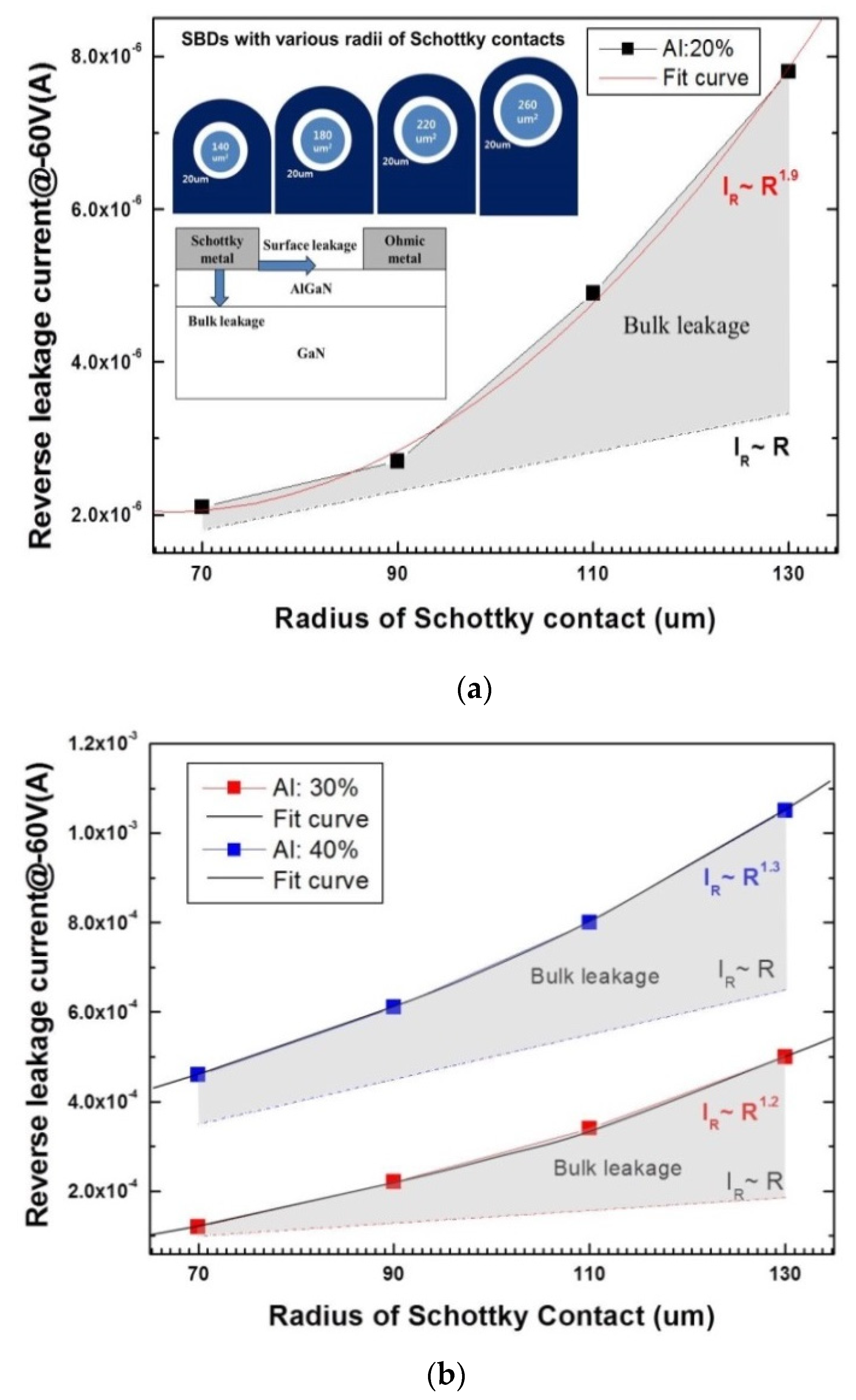
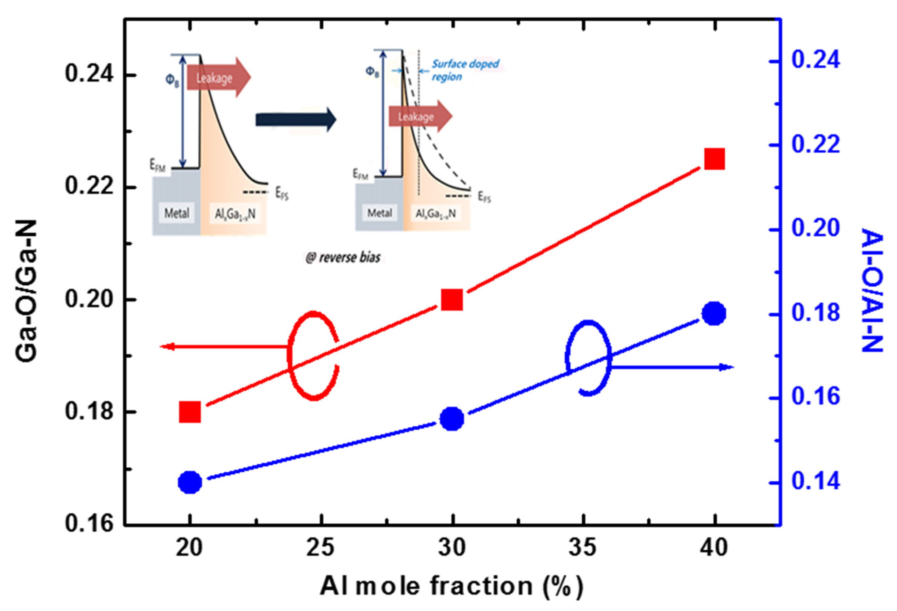
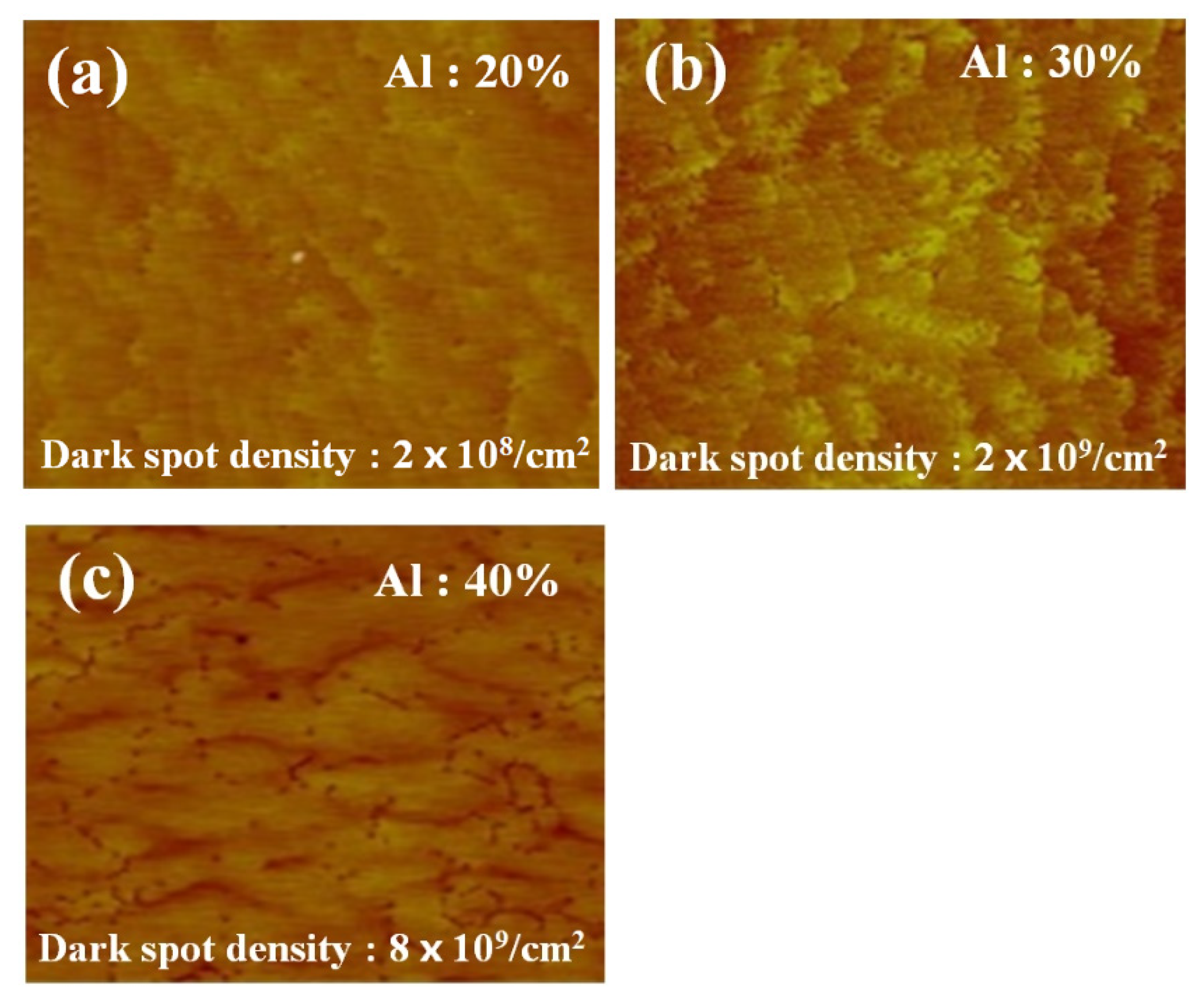
3.1. Effect of Al Composition on Characteristics of AlGaN/GaN SBDs

Figure 2 shows the reverse leakage current of the SBDs at −60 V according to the radius of the anode electrode. The radius of the Schottky anode contact on the AlGaN barrier layer is changed from 70 to 130 μm with a fixed distance of 20 μm between the anode and the cathode. The leakage current of the AlxGa1−xN/GaN SBD with x = 0.2 presents at least two orders’ lower value compared to those of the devices with x = 0.3 and 0.4. It is also interesting that the leakage current of the device with x = 0.2 exponentially increases with the anode area of the SBD (IR ∝ R1.9, R: radius). However, the leakage currents of the devices with x = 0.3 and 0.4 are considerably higher, but are approximately proportional to the perimeter of the anode area of SBD with dependence of approximately R1.2 ~ R1.3.
To analyze the leakage current mechanism, the circular-type SBDs in the inset of Figure 2a have two leakage components: (1) bulk leakage current induced by electrons tunneling through the AlGaN barrier layer and (2) the surface leakage current caused by the surface states of the unpassivated AlGaN layer. Considering the anode area of SBD becomes zero, total leakage current consists of only the surface leakage current. The surface leakage current is estimated from the y-intercept of Figure 2 and linearly increases with the increased radius of Schottky contact (the dashed lines of IR ~ R1.0 in Figure 2) because the space area between the anode and the cathode is linearly increasing. On the other hand, the bulk leakage current is clearly observed from the difference of surface leakage current on total leakage current (grey color in Figure 2). From the radius-dependent variation of leakage currents, the device with x = 0.2 is dominated with the bulk leakage component in vertical direction, whereas the surface leakage component for the other devices prevails.
In order to further investigate the large bulk leakage current for the device with higher Al composition, the X-ray photoelectron spectroscopy (XPS) spectra was measured at the surface of AlxGa1−xN (x = 0.2, 0.3, and 0.4), as shown in Figure 3. As increasing Al composition, both intensity ratios for (Ga−O)/(Ga−N) and (Al−O)/(Al−N) enhance, which indicates that the AlGaN layer easily absorbs the oxygen atoms according to the high Al composition. Because the oxygen impurity plays a role of donorlike states in the AlGaN material, the surface of the AlGaN layer is leaky [16,17]. These donors also narrow the AlGaN barrier, which leads to an increase in the electron tunneling probability and thus deteriorates the reverse bulk leakage current in the inset of Figure 3.
In addition, the high Al composition leads to large V-shaped defect (dark spot) density in the AlGaN layer due to the huge lattice mismatch between the AlGaN and GaN layer [6,18,19]. While the Al composition is 20, 30, and 40%, the corresponding defect density increased to 2, 20, and 80 × 108 /cm2, respectively, as shown in Figure 4. The estimated average size of dark spots for AlxGa1−xN (x = 0.2, 0.3, 0.4) were also about 8, 20, and 100 nm, respectively. In AlGaN layers grown on the GaN layer, the size and shape of dark spots were affected by the threading dislocation in GaN buffer, Al composition in AlGaN, tensile strain, and growth conditions, which would increase the probability of the trap-related tunneling and thus impact the bulk leakage current [20].

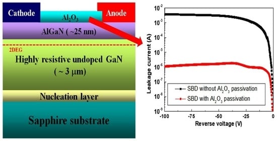
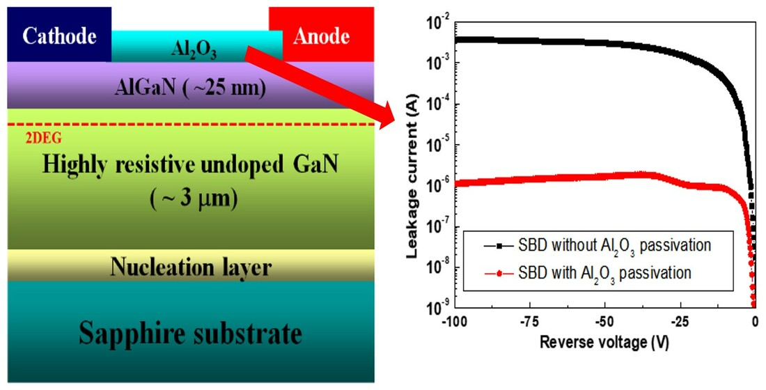
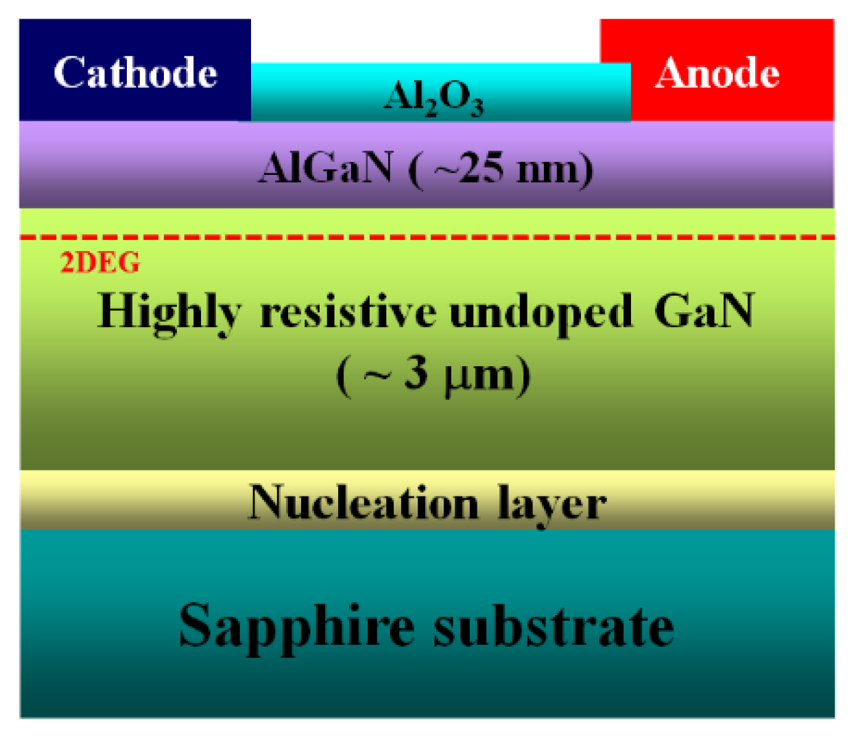
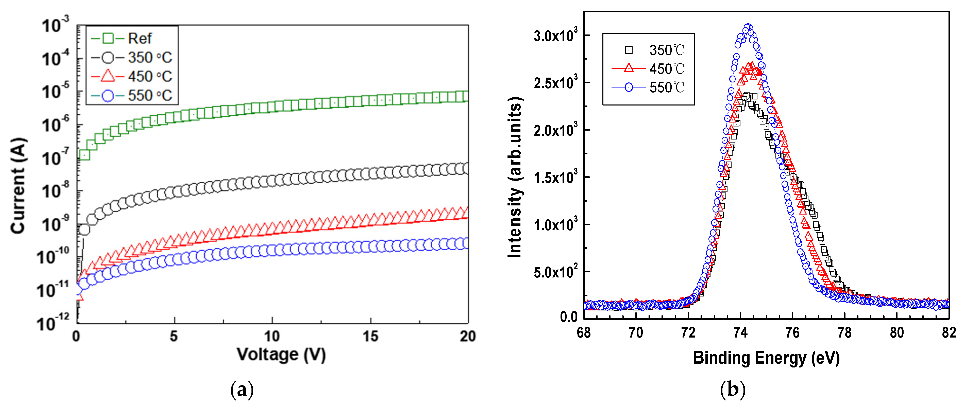
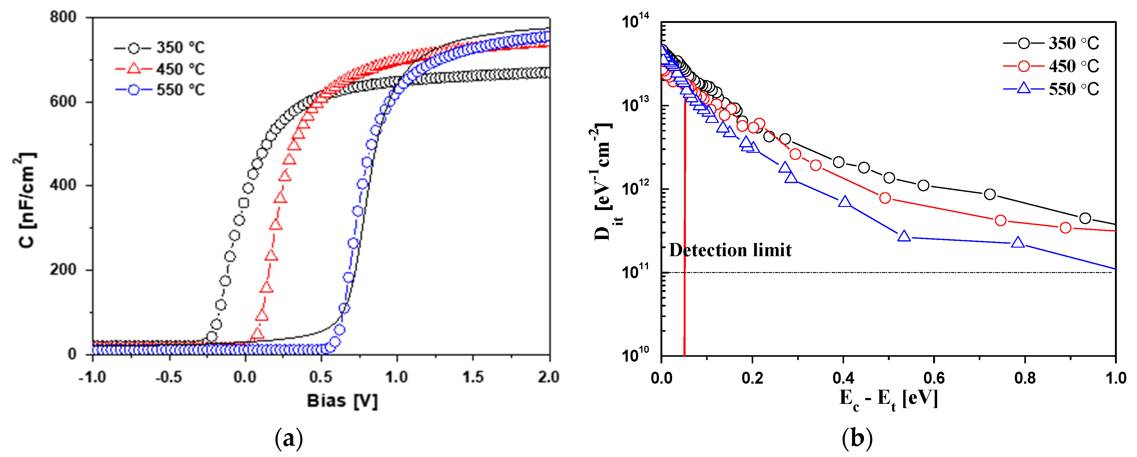
3.2. High Temperature Al2O3 Dielectric Layers

For obtaining the improved interface properties between Al2O3 and GaN as well as the good dielectric property of Al2O3 itself, 30 nm-thick Al2O3 dielectric layers were deposited on 2 μm-thick undoped GaN layer with varying the deposition temperature from 350 °C to 550 °C. Figure 5a shows the current–voltage (I–V) characteristics of Al2O3/GaN metal-insulator-semiconductor (MIS) capacitors. The diameter of the inner circular contact and an interelectrode distance is 40 μm and 20 μm, respectively. The leakage current of the diode with Al2O3 passivation layer deposited at 350 °C was measured as 30 nA at 20 V, much lower than that of the reference diode without the passivation layer (10 μA). Moreover, when the temperature increases to 550 °C, the leakage current is further decreased to 0.1 nA.
The chemical properties of the Al2O3 films according to the deposition temperature were investigated by XPS, as shown in Figure 5b. The XP spectra of Al2O3/GaN samples can be achieved by Ar+ ion gun etching and measuring in a sequence. The obtained results show that the peak position of the Al 2p for all samples is located 74.3 eV, consistent with that of crystalline Al2O3 (sapphire) [21], which indicates that the Al–O bond is dominant in the atomic configuration of Al2O3. On the other hand, the sample deposited at 350 °C exhibits lower Al 2p peak than those of the other samples and also a satellite peak near the binding energy of 76 eV. This explains that the different chemical state such as AlOx may exist in the sample deposited at 350 °C due to the insufficient thermal energy, which leads to the degraded device performances such as severe hysteresis and high current collapses [22].
Figure 6a shows the capacitance–voltage (C–V) characteristics of the Al2O3/GaN MIS capacitors measured at 1 MHz including the calculated ideal curve (the dashed line). The effective fixed charge (Qeff) in the dielectric layer is determined by the parallel shift of the measured curve compared to the ideal one using the following equation,
  Q eff = C dielectric Δ V FB
where the capacitance of the dielectric layer per unit area of Cdielectric, and the flat-band shift of the measured flat-band voltage from the ideal curve of ΔVFB [6]. The calculated flat band capacitance, CFB = Ksε0/LD (where LD is Debye length) for the Al2O3 layer deposited at 350 °C, 450 °C, and 550 °C is 160 nF·cm−2, 172 nF·cm−2, and 185 nF·cm−2, respectively. The corresponding values of the estimated VFB shift were −0.65 V, −0.4 V, and −0.02 V, respectively, which results in Qeff of −2.85 × 1012 cm−2, −1.7 × 1012 cm−2, and −1.2 × 1011 cm−2, respectively. As the deposition temperature increases, the Qeff results in the decreased fixed charge density at the interface and hence higher VFB shift in MIS capacitors.
Figure 6b shows the distribution of the interface state density (Dit) at the Al2O3/GaN interface calculated by the Terman method [23].
  D it = C ox q ( dV G dQ S 1 ) C s q = C ox q d Δ V G dQ s
where the electronic charge of q, the applied gate bias of VG, the surface potential of QS, and the shift of the measured gate voltage, (VG,measured), from the ideal value, (VG,ideal) of {ΔVG = (VG,measured) − (VG,ideal)} [7]. The corresponding surface potential is used to determine the position of the interface states in the bandgap. The estimated interface trap density at 0.4 eV below Ec was 4.5 × 1012 cm−2·eV−1, 5.2 × 1011 cm−2·eV−1, and 1.7 × 1011 cm−2·eV−1 for the Al2O3 layer deposited at 350 °C, 450 °C, and 550 °C, respectively. This clearly indicates that high temperature ALD deposition passivation is effective in decreasing the interface states.

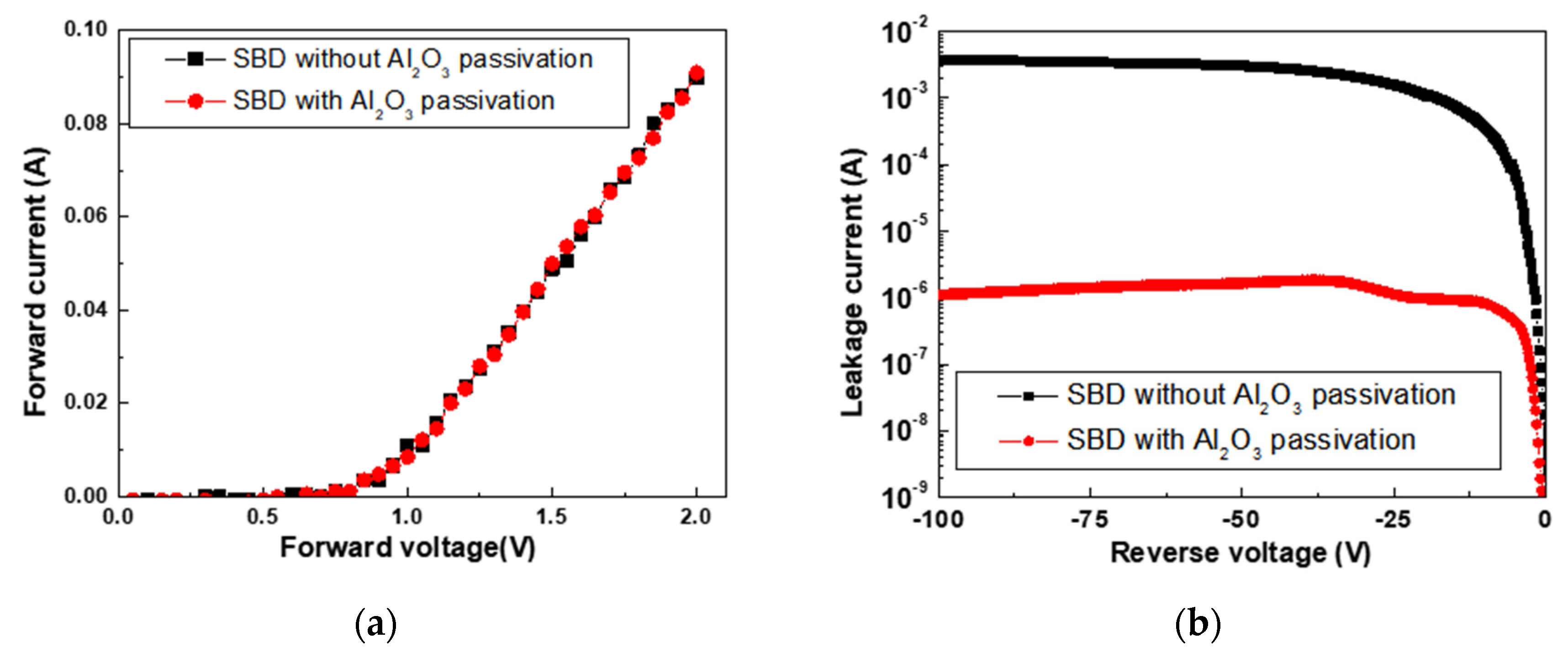
3.3. I–V Curves of the Fabricated AlGaN/GaN SBDs

Even though the AlxGa1−xN/GaN SBD with x = 0.2 mitigates the reverse leakage current, it demonstrated the reduced on-current and low switching speed with the severe radius-dependent variation of leakage currents (Figure 2a) [24]. Therefore, the as-grown AlxGa1−xN/GaN layer with x = 0.3 was used to fabricate the SBD. However, it still suffered from large bulk and surface leakage currents. The bulk leakage current can be improved by applying large work function metal or using wide bandgap material as a barrier layer [14]. To alleviate the surface leakage current, a 30 nm-thick Al2O3 dielectric layer with the deposition temperature of 550 °C was deposited on the AlGaN/GaN SBD. The reference sample without Al2O3 layer was also prepared.
Figure 7 showed the I–V curves of the fabricated AlGaN/GaN SBDs (the radius of anode of 200 μm and the distance between the anode and the cathode of 20 μm). The forward turn-on voltages of about 0.8 V for the fabricated SBDs with/without the Al2O3 layer were exhibited in Figure 7a. The I–V curves were evaluated using the following equations [25]:
I = I 0 [ e x p ( q V n k T ) 1 ]   w i t h   I 0 = A A * T 2 e x p ( q Φ B k T )
where the ideality factor of n, the thermal energy of kT, the Schottky barrier height of ΦB, the contact area of A, and the effective Richardson constant of A*. The extracted ideality factor was 1.63 for the SBD without passivation layer, but it was reduced to 1.41 for the SBD with Al2O3 passivation layer, which is believed to be due to the reduced surface leakage current.
The leakage current of the SBD without passivation layer was as high as 3.2 mA at −60 V, while the leakage current of the SBD with Al2O3 passivation layer was dramatically decreased to 1.5 μA, as shown in Figure 7b. It is attributed that the high quality Al2O3 layer deposited at high temperature decreases the oxygen absorption into the AlGaN layer from air exposure, which is related to the reduction of the leakage current of the SBD, as mentioned before. Moreover, the surface states on the AlGaN surface without passivation layer are responsible for the surface leakage current. After deposition of the Al2O3 passivation layer, most donorlike states were occupied and thus the surface leakage current suppresses.

4. Conclusions

To reduce reverse leakage current in SBDs, we have proposed, fabricated, and characterized an AlGaN/GaN-SBD with high Al composition and high temperature (550 °C) deposited Al2O3 passivation layer. The fabricated device showed a nearly 3-fold reduction in the leakage current compared to the reference device without the Al2O3 passivation layer. The effective surface passivation with a high temperature Al2O3 layer attributes to greatly reducing the surface leakage current caused by the suppression of the donorlike surface states. The proposed SBD has a great potential in electronics for applying the high power switching systems.

Author Contributions

Writing—review and editing, J.-H.L. (Jae-Hoon Lee) and K.-S.I.; investigation, J.-H.L. (Jung-Hee Lee) and K.-S.I.; synthesis, J.-H.L. (Jae-Hoon Lee); fabrication, J.-H.L. (Jae-Hoon Lee) and K.-S.I.; data collection of DC, K.-S.I.; All authors have read and agreed to the published version of the manuscript.

Funding

This research received no external funding.

Acknowledgments

This work was supported by the National Research Foundation of Korea (NRF) funded by the Ministry of Education, Science and Technology (MEST) (No. NRF-2018R1A6A1A03025761, NRF-2019R1I1A1A01064011). The authors would like to thank to Jong Kyu Kim of Pohang University of Science and Technology for the useful measurements and discussions.

Conflicts of Interest

The authors declare no conflict of interest.

References

  1. Nakamura, S.; Senoh, M.; Nagahama, S.; Iwasa, N.; Yamada, T.; Mat-sushita, T.; Sugimoto, Y.; Kiyoku, H. High-Power, Long-Lifetime InGaN Multi-Quantum-Well-Structure Laser Diodes. Jpn. J. Appl. Phys. 1997, 36, L1059. [Google Scholar] [CrossRef]
  2. Lee, J.H.; Lee, D.Y.; Oh, B.W.; Lee, J.H. Comparison of InGaN-based LEDs grown on conventional sapphire and cone-shape-patterned sapphire substrate. IEEE Trans. Electron Dev. 2010, 57, 157. [Google Scholar] [CrossRef]
  3. Ambacher, O.; Smart, J.; Shealy, J.R.; Weimann, N.G.; Chu, K.; Murphy, M.; Schaff, W.J.; Eastman, L.F.; Dimitrov, R.; Wittmer, L.; et al. Two-dimensional electron gases induced by spontaneous and piezoelectric polarization charges in N and Ga-face AlGaN/GaN heterostructures. J. Appl. Phys. 1999, 85, 3222. [Google Scholar] [CrossRef] [Green Version]
  4. Wu, Y.-F.; Kapolnek, D.; Ibbetson, J.P.; Parikh, P.; Keller, B.P.; Mishra, U.K. Very-high power density AlGaN/GaN HEMTs. IEEE Electron Dev. Lett. 2001, 48, 586. [Google Scholar]
  5. Uemoto, Y.; Hikita, M.; Ueno, H.; Matsuo, H.; Ishida, H.; Yanagihara, M.; Ueda, T.; Tanaka, T.; Ueda, D. Gate injection transistor (GIT)-A normally-off AlGaN/GaN power transistor using conductivity modulation. IEEE Trans. Electron Dev. 2007, 54, 3393. [Google Scholar] [CrossRef]
  6. Lee, J.-H.; Im, K.-S.; Kim, J.K.; Lee, J.-H. Performance of recessed anode AlGaN/GaN Schottky barrier diode passivated with high-temperature atomic layer-deposited Al2O3 layer. IEEE Trans. Electron Dev. 2019, 66, 324. [Google Scholar] [CrossRef]
  7. Hasegawa, H.; Oyama, S. Mechanism of anomalous current transport in n-type GaN Schottky contacts. J. Vac. Sci. Technol. B 2002, 20, 1647. [Google Scholar] [CrossRef]
  8. Klein, P.B.; Binari, S.C.; Ikossi, K.; Wickenden, A.E.; Koleske, D.D.; Henry, R.L. Current collapse and the role of carbon in AlGaN/GaN high electron mobility transistors grown by metalorganic vapor-phase epitaxy. Appl. Phys. Lett. 2001, 79, 3527. [Google Scholar] [CrossRef]
  9. Vetury, R.; Zhang, N.Q.; Keller, S.; Mishra, U.K. The impact of surface states on the DC and RF characteristics of AlGaN/GaN HFETs. IEEE Trans. Electron Dev. 2001, 48, 560. [Google Scholar] [CrossRef]
  10. Hasegawa, H.; Inagaki, T.; Ootomo, S.; Hashizume, T. Mechanisms of current collapse and gate leakage currents in AlGaN/GaN heterostructure field effect transistors. J. Vac. Sci. Technol. B 2003, 21, 1844. [Google Scholar] [CrossRef] [Green Version]
  11. Simin, G.; Koudymov, A.; Fatima, H.; Zhang, J.; Yang, J.; Khan, M.A.; Hu, X.; Tarakji, A.; Gaska, R.; Shur, M. SiO2/AlGaN/InGaN/GaN MOSDHFETs. IEEE Electron Dev. Lett. 2002, 23, 458. [Google Scholar] [CrossRef]
  12. Onojima, N.; Higashiwaki, M.; Suda, J.; Kimoto, T.; Mimura, T.; Matsui, T. Reduction in potential barrier height of AlGaN/GaN heterostructures by SiN passivation. J. Appl. Phys. 2007, 101, 043703. [Google Scholar] [CrossRef]
  13. Wang, C.; Maeda, N.; Hiroki, M.; Yokoyama, H.; Watanabe, N.; Makimoto, T.; Enoki, T.; Kobayashi, T. Mechanism of superior suppression effect on gate current leakage in ultrathin Al2O3/Si3N4 bilayer-based AlGaN/GaN insulated gate heterostructure field-effect transistors. Jpn. J. Appl. Phys. 2006, 45, 40. [Google Scholar] [CrossRef]
  14. Lee, J.-H.; Jeong, J.-H.; Lee, J.-H. Enhanced Electrical Characteristics of AlGaN-Based SBD With In Situ Deposited Silicon Carbon Nitride Cap Layer. IEEE Electron Dev. Lett. 2012, 33, 492. [Google Scholar] [CrossRef]
  15. Lee, J.-H.; Lee, M.-B.; Hahm, S.-H.; Lee, Y.-H.; Lee, J.-H.; Bae, Y.-H.; Cho, H.K. Growth of Semi-insulating GaN Layer by Controlling Size of Nucleation Sites for SAW Device Applications. MRS Internet J. Nitride Semicond. Res. 2003, 8, 5. [Google Scholar] [CrossRef]
  16. Kim, J.K.; Jang, H.W.; Lee, J.L. Current conduction mechanism of Pt/GaN and Pt/Al0.35 Ga0.65N Schottky diodes. J. Appl. Phys. 2003, 94, 7201. [Google Scholar] [CrossRef] [Green Version]
  17. Kotani, J.; Kaneko, M.; Hasegawa, H.; Hashizume, T. Large reduction of leakage currents in AlGaN Schottky diodes by a surface control process and its mechanism. J. Vac. Sci. Technol. B 2006, 24, 2148. [Google Scholar] [CrossRef] [Green Version]
  18. Ma, J.; Lu, X.; Jiang, H.; Liu, C.; Lau, K.M. In situ growth of SiNx as gate dielectric and surface passivation for AlN/GaN heterostructures by metalorganic chemical vapor deposition. Appl. Phys. Exp. 2014, 7, 091002. [Google Scholar] [CrossRef]
  19. Pakula, K.; Bozek, R.; Baranowski, J.M.; Jasinski, J.; Liliental-Weber, Z. Reduction of dislocation density in heteroepitaxial GaN: Role of SiH4 treatment. J. Cryst. Growth 2004, 267, 1. [Google Scholar] [CrossRef]
  20. Miller, E.J.; Schaadt, D.M.; Yu, E.T. Origin and microscopic mechanism for suppression of leakage currents in Schottky contacts to GaN grown by molecular-beam epitaxy. J. Appl. Phys. 2003, 94, 7611. [Google Scholar] [CrossRef] [Green Version]
  21. Faraci, G.; Rosa, S.; Hwu, Y.; Margaritondo, G. Al intermediate oxidation states observed by core level photoemission spectroscopy. J. Appl. Phys. 1995, 78, 4091. [Google Scholar] [CrossRef]
  22. Kang, H.-S.; Reddy, M.S.P.; Kim, D.-S.; Kim, K.-W.; Ha, J.-B.; Lee, Y.S.; Choi, H.-C.; Lee, J.-H. Effect of oxygen species on the positive flat-band voltage shift in Al2O3/GaN metal–insulator–semiconductor capacitors with post-deposition annealing. J. Phys. D Appl. Phys. 2013, 46, 155101. [Google Scholar] [CrossRef]
  23. Terman, L.M. An investigation of surface states at a silicon/silicon oxide interface employing metal-oxide-silicon diodes. Solid-State Electron. 1962, 5, 285. [Google Scholar] [CrossRef]
  24. Lee, J.-H.; Park, C.; Im, K.-S.; Lee, J.-H. AlGaN/GaN-based lateral-type schottky barrier diode with very low reverse recovery charge at high temperature. IEEE Trans. Electron Dev. 2013, 60, 3032. [Google Scholar] [CrossRef]
  25. Cheung, S.K.; Cheung, N.W. Extraction of Schottky diode parameters from forward current–voltage characteristics. Appl. Phys. Lett. 1986, 49, 85. [Google Scholar] [CrossRef]
Figure 1. A schematic view of the proposed Schottky barrier diodes (SBD), including epitaxial layers and thickness.
Crystals 11 00087 g001
Figure 2. Reverse leakage current for AlxGa1−xN/GaN SBD with Al composition of 0.2 (a), 0.3 (b), and 0.4 (b) at −60 V according to size of Schottky diameter. The inset of (a) shows the schematic illustrations of SBDs with various radius of Schottky contacts including vertical and lateral leakage current path.
Crystals 11 00087 g002
Figure 3. Intensity ratios of [Ga−O]/[Ga−N] (left Y-axis) and [Al−O]/[Al−N] (right Y-axis) as a function of the Al composition. The inset shows the schematic energy band diagrams of metal/AlGaN and tunneling probability of the electrons through the narrowed barrier width at reverse bias.
Crystals 11 00087 g003
Figure 4. Atomic force microscope (AFM) images of the AlGaN surface according to Al compositions of (a) 20%, (b) 30%, and (c) 40%.
Crystals 11 00087 g004
Figure 5. (a) Current–voltage (I–V) characteristics of diode and (b) X-ray photoelectron spectroscopy (XPS) depth profile analysis of Al2O3/GaN interface by varying the atomic layer deposition (ALD) growth temperature from 350 °C to 550 °C.
Crystals 11 00087 g005
Figure 6. (a) CV characteristics of the Al2O3/GaN MIS capacitor and (b) interface state density distributions of the Al2O3/GaN MIS capacitors by varying the ALD growth temperature from 350 °C to 550 °C.
Crystals 11 00087 g006
Figure 7. (a) Forward and (b) reverse I–V curves of the AlGaN/GaN SBDs with and without ALD Al2O3 passivation layer deposited at 550 °C.
Crystals 11 00087 g007
Publisher’s Note: MDPI stays neutral with regard to jurisdictional claims in published maps and institutional affiliations.

